


IRG7PH42UD1PBF
IGBT, 85 A, 1.7 V, 313 W, 1.2 kV, TO-247AC, 3 Pins
- Manufacturer: INFINEON
- Product type: Single IGBTs
- DC Collector Current:85A; Collector Emitter Saturation Voltage Vce(on):1.7V; Power Dissipation Pd:313W; Collector Emitter Voltage V(br)ceo:1.2kV; Transistor Case Style:TO-247AC; No. of
- No. of Pins: 3Pins
- Product Range: -
- Power Dissipation: 313W
- Transistor Mounting: Through Hole
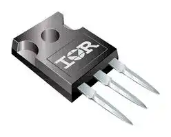
- Transistor Case Style: TO-247AC
- Operating Temperature Max: 150°C
- Continuous Collector Current: 85A
- Collector Emitter Voltage Max: 1.2kV
- Collector Emitter Saturation Voltage: 1.7V
| Delivery and price | |
|---|---|
| Units per pack | 500 |
| Price | 3.63 € |
| Current stock | 10+ |
| Lead time | 30 days |
IRG7PH42UD1PbF IRG7PH42UD1-EP

## _**INSULATED GATE BIPOLAR TRANSISTOR WITH ULTRA-LOW VF DIODE FOR INDUCTION HEATING AND SOFT SWITCHING APPLICATIONS**_

## **Features**

- Low VCE (ON) trench IGBT technology

- Low switching losses

- Square RBSOA

- Ultra-low VF Diode

- 1300Vpk repetitive transient capacity

- 100% of the parts tested for ILM

- Positive VCE (ON) temperature co-efficient

- Tight parameter distribution

> C VCES = 1200V I NOMINAL = 30A

> G T = 150°C J(max) E n-channel VCE(on) typ. = 1.7V

- Lead free package

## **Benefits**

- Device optimized for induction heating and soft switching applications

- High Efficiency due to Low VCE(on), low switching losses and Ultra-low VF

**==> picture [176 x 84] intentionally omitted <==**

**----- Start of picture text -----**<br>
G  G<br>E  E<br>C  C<br>G  G<br>TO-247AC TO-247AD<br>IRG7PH42UD1PbF IRG7PH42UD1-EP<br>**----- End of picture text -----**<br>


- Rugged transient performance for increased reliability

- Excellent current sharing in parallel operation

|Excellent current sharing in parallel operation<br>Low EMI|Excellent current sharing in parallel operation||**G**<br>**C**<br>**E**<br>Gate<br>Collector<br>Emitter<br>~~———~~|**G**<br>**C**<br>**E**<br>Gate<br>Collector<br>Emitter<br>~~———~~|**G**<br>**C**<br>**E**<br>Gate<br>Collector<br>Emitter<br>~~———~~|
|---|---|---|---|---|---|
|**Base part number**|**Package Type**|**Standard Pack**|||**Orderable Part Number**|
|||**Form**|**Quantity**|||
|IRG7PH42UD1PbF|TO-247AC|Tube|25||IRG7PH42UD1PbF|
|IRG7PH42UD1-EP|TO-247AD|Tube|25||IRG7PH42UD1-EP|


- Low EMI

**Absolute Maximum Ratings**

|**Absolute Maximum Ratings**|**Absolute Maximum Ratings**<br>**Parameter**|**Max.**|**Units**|
|---|---|---|---|
|VCES<br>~~oe~~|Collector-to-Emitter Voltage<br>~~oe~~|1200<br>~~oe~~|V<br>~~oe~~|
|V(BR)Transient<br>~~oe~~|Repetitive Transient Collector-to-Emitter Voltage<br>~~oe~~|1300<br>~~oe~~||
|IC@ TC= 25°C<br>~~oe~~<br>~~ee~~|Continuous Collector Current<br>~~oe~~<br>~~ee~~|85<br>~~oe~~<br>~~ee~~|A<br>~~oe~~<br>~~ee~~<br>~~ae~~|
|IC@ TC= 100°C<br>~~ee~~<br>~~ee~~|Continuous Collector Current<br>~~ee~~|45<br>~~ee~~<br>~~ae~~||
|INOMINAL<br>~~ee~~<br>~~ee~~|Nominal Current<br>~~ee~~|30<br>~~ee~~<br>~~ae~~||
|ICM<br>~~ee~~<br>~~ee~~<br>~~a~~|Pulse Collector Current, VGE=15V<br>~~ee~~<br>~~a~~|200<br>~~ee~~<br>~~ae~~<br>~~a~~||
|ILM<br>~~ee~~<br>~~ee~~<br>~~©~~<br>~~a~~|Clamped Inductive Load  Current,  VGE=20V<br>~~ee~~<br>~~©~~<br>~~a~~|120<br>~~ee~~<br>~~ae~~<br>~~©~~||
|IF@ TC= 25°C<br>~~ee~~<br>~~a~~<br>~~ee~~|Diode Continous Forward Current<br>~~ee~~<br>~~a~~<br>~~ee~~|70<br>~~ee~~<br>~~ee~~||
|IF@ TC= 100°C<br>~~ee~~<br>~~a~~<br>~~ee~~<br>~~a~~<br>~~i~~|Diode Continous Forward Current<br>~~ee~~<br>~~a~~<br>~~ee~~<br>~~a~~<br>|35<br>~~ee~~<br>~~ee~~||
|IFRM<br>~~ee~~<br>~~a~~<br>~~i~~|Diode Repetitive Peak Forward Current<br>~~ee~~<br>~~a~~<br>|120<br>~~ee~~||
|VGE<br>~~a~~<br>~~i~~<br>~~SS~~|Continuous Gate-to-Emitter Voltage<br>~~a~~<br>~~a~~|±30|V|
|PD@ TC= 25°C<br>~~a~~<br>~~i ~~<br>~~SS~~|Maximum Power Dissipation<br>~~a~~<br> ~~a~~|313|W<br>~~ee~~|
|PD@ TC= 100°C<br> <br>~~SS~~<br>~~ee~~|Maximum Power Dissipation<br> ~~a~~<br>~~ee~~|125<br>~~ee~~||
|TJ<br>TSTG<br> <br>~~SS~~<br>~~ee~~<br>~~|~~|Operating Junction and<br>Storage Temperature Range<br> ~~a~~<br>~~ee~~<br>~~CO~~|-55 to +150<br>~~ee~~<br>~~CO~~|°C<br>~~ee~~|
|~~ee~~<br>~~|~~<br>~~fF~~|SolderingTemperature,for 10 sec.<br>~~ee~~<br>~~CO~~|300 (0.063in.(1.6mm)fromcase)<br>~~ee~~<br>~~CO~~||
|~~ee~~<br>~~|~~<br>~~fF~~|MountingTorque, 6-32or M3 Screw<br>~~ee~~<br>~~CO~~|10lbf·in(1.1 N·m)<br>~~ee~~<br>~~CO~~|~~ee~~|


1

www.irf.com   © 2013 International Rectifier                                                 April 24, 2013

IRG7PH42UD1PbF/IRG7PH42UD1-EP

## **Electrical Characteristics @ TJ = 25°C (unless otherwise specified)**

||**Parameter**|**Min.**|**Typ.**|**Max.**|**Units**|**Conditions**|
|---|---|---|---|---|---|---|
|V(BR)CES|Collector-to-Emitter Breakdown Voltage|1200|—|—|V|VGE= 0V,IC= 100μA�|
|ΔV(BR)CES/ΔT J|Temperature Coeff. of Breakdown Voltage|—|1.2|—|V/°C|VGE= 0V,IC= 2.0mA(25°C-150°C)|
|VCE(on)|Collector-to-Emitter Saturation Voltage|—|1.7|2.0|V|IC= 30A,VGE= 15V,TJ= 25°C|
|||—|2.0|—||IC= 30A,VGE= 15V,TJ= 150°C|
|VGE(th)|Gate Threshold Voltage|3.0|—|6.0|V|VCE= VGE,IC= 1.0mA<br>VCE= 50V,IC= 30A,PW = 80μs|
|gfe|Forward Transconductance|—|32|—|S||
|ICES|Collector-to-Emitter Leakage Current|—|1.0|100|μA|VGE= 0V,VCE= 1200V|
|||—|230|—||VGE= 0V,VCE= 1200V,TJ= 150°C|
|VFM|Diode Forward Voltage Drop|—|1.15|1.30|V|IF= 30A|
|||—|1.10|—||IF= 30A,TJ= 150°C|
|IGES|Gate-to-Emitter LeakageCurrent|—|—|±100|nA|VGE= ±30V|


## **Switching Characteristics @ TJ = 25°C (unless otherwise specified)**

||**Parameter**|**Min.**|**Typ.**|**Max.**|**Units**|**Conditions**|
|---|---|---|---|---|---|---|
|Qg|Total Gate Charge(turn-on)|—|180|270|nC|IC= 30A<br>VGE= 15V<br>VCC= 600V|
|Qge|Gate-to-Emitter Charge(turn-on)|—|24|36|||
|Qgc|Gate-to-Collector Charge(turn-on)|—|70|110|||
|Eoff|Turn-Off Switching Loss|—|1210|1450|μJ|IC= 30A, VCC= 600V, VGE= 15V<br>RG= 10Ω, L = 200μH,TJ= 25°C<br>Energylosses include tail|
|td(off)|Turn-Off delaytime|—|270|290|ns|IC= 30A, VCC= 600V, VGE= 15V<br>RG= 10Ω,L = 200μH,TJ= 25°C|
|tf|Fall time|—|35|43|||
|Eoff|Turn-Off Switching Loss|—|1936|—|μJ|IC= 30A, VCC= 600V, VGE= 15V<br>RG= 10Ω, L = 200μH,TJ= 150°C<br>Energylosses include tail|
|td(off)|Turn-Off delaytime|—|300|—|ns|IC= 30A, VCC= 600V, VGE= 15V<br>RG= 10Ω,L = 200μH,TJ= 150°C|
|tf|Fall time|—|160|—|||
|Cies|InputCapacitance|—|3390|—|pF|VGE= 0V<br>VCC= 30V<br>f = 1.0Mhz|
|Coes|OutputCapacitance|—|130|—|||
|Cres|Reverse TransferCapacitance|—|83|—|||
|RBSOA|Reverse Bias Safe Operating Area|FULL SQUARE||||TJ= 150°C, IC= 120A<br>VCC= 960V, Vp =1200V<br>Rg= 10Ω,VGE= +20V to 0V|


## **Notes:**

- VCC = 80% (VCES), VGE = 20V, L = 22μH, RG = 10 Ω.

- Pulse width limited by max. junction temperature.

- Refer to AN-1086 for guidelines for measuring V(BR)CES safely.

- R θ is measured at TJ of approximately 90°C.

- Calculated continuous current based on maximum allowable junction temperature. Bond wire current limit is 78A. Note that current limitations arising from heating of the device leads may occur with some lead mounting arrangements.

- FBSOA operating conditions only

- VGE = 0V, TJ = 75°C �� PW ≤ 10μs �

www.irf.com   © 2013 International Rectifier                                                April 24, 2013

2

## IRG7PH42UD1PbF/IRG7PH42UD1-EP

**==> picture [206 x 658] intentionally omitted <==**

**----- Start of picture text -----**<br>
100<br>LIMITED BY PACKAGE<br>80<br>60<br>40<br>20<br>0<br>25 50 75 100 125 150<br> TC,  Case Temperature (°C)<br>Fig. 1  - Maximum DC Collector Current vs.<br>Case Temperature<br>1.0<br>IC = 1.0mA<br>0.9<br>0.8<br>0.7<br>0.6<br>0.5<br>25 50 75 100 125 150<br>TJ , Temperature (°C)<br>Fig. 3  - Typical Gate Threshold Voltage<br>(Normalized) vs. Junction Temperature<br>120<br>VGE = 18V<br>100<br>VGE = 15V<br>VGE = 12V<br>80<br>VGE = 10V<br>VGE = 8.0V<br>60<br>40<br>20<br>0<br>0 2 4 6 8 10<br> VCE (V)<br>VGE(th), Gate Threshold Voltage (Normalized)<br>IC,  Collector Current (A)<br>ICE (A)<br>**----- End of picture text -----**<br>


**Fig. 5** - Typ. IGBT Output Characteristics TJ = -40°C; tp = 80μs

**==> picture [205 x 193] intentionally omitted <==**

**----- Start of picture text -----**<br>
350<br>300<br>250<br>200<br>150<br>100<br>50<br>0<br>25 50 75 100 125 150<br> TC (°C)<br>Ptot (W)<br>**----- End of picture text -----**<br>


**Fig. 2** - Power  Dissipation vs. Case Temperature

**==> picture [208 x 194] intentionally omitted <==**

**----- Start of picture text -----**<br>
1000<br>100<br>10<br>1<br>10 100 1000 10000<br>VCE (V)<br>IC (A)<br>**----- End of picture text -----**<br>


**Fig. 4** - Reverse Bias SOA TJ = 150°C; VGE = 20V

**==> picture [199 x 197] intentionally omitted <==**

**----- Start of picture text -----**<br>
120<br>VGE = 18V<br>100 VGE = 15V<br>VGE = 12V<br>80 VGE = 10V<br>VGE = 8.0V<br>60<br>40<br>20<br>0<br>0 2 4 6 8 10<br> VCE (V)<br>ICE (A)<br>**----- End of picture text -----**<br>


**Fig. 6** - Typ. IGBT Output Characteristics TJ = 25°C; tp = 80μs

www.irf.com   © 2013 International Rectifier                                                April 24, 2013

3

IRG7PH42UD1PbF/IRG7PH42UD1-EP

**==> picture [199 x 198] intentionally omitted <==**

**----- Start of picture text -----**<br>
120<br>VGE = 18V<br>100 V GE  = 15V<br>VGE = 12V<br>VGE = 10V<br>80<br>VGE = 8.0V<br>60<br>40<br>20<br>0<br>0 2 4 6 8 10<br> VCE (V)<br>ICE (A)<br>**----- End of picture text -----**<br>


**Fig. 7** - Typ. IGBT Output Characteristics TJ = 150°C; tp = 80μs

**==> picture [203 x 454] intentionally omitted <==**

**----- Start of picture text -----**<br>
20<br>18<br>16<br>14<br>12 I CE  = 15A<br>10 ICE = 30A<br>ICE = 60A<br>8<br>6<br>4<br>2<br>0<br>5 10 15 20<br> VGE (V)<br>Fig. 9  - Typical VCE vs. VGE<br>TJ = -40°C<br>20<br>18<br>16<br>14<br>12<br>ICE = 15A<br>10<br>ICE = 30A<br>8 I CE  = 60A<br>6<br>4<br>2<br>0<br>5 10 15 20<br> VGE (V)<br>Fig. 11  - Typical VCE vs. VGE<br>TJ = 150°C<br>VCE (V)<br>VCE (V)<br>**----- End of picture text -----**<br>


**==> picture [196 x 428] intentionally omitted <==**

**----- Start of picture text -----**<br>
140<br>120<br>25°C<br>150°C<br>100<br>80<br>60<br>40<br>20<br>0<br>0.0 0.5 1.0 1.5 2.0<br> VF (V)<br>Fig. 8  - Typ. Diode Forward Voltage Drop<br>Characteristics<br>20<br>18<br>16<br>14<br>12<br>ICE = 15A<br>10<br>ICE = 30A<br>8 I CE  = 60A<br>6<br>4<br>2<br>0<br>5 10 15 20<br> VGE (V)<br>IF (A)<br>VCE (V)<br>**----- End of picture text -----**<br>


**==> picture [205 x 224] intentionally omitted <==**

**----- Start of picture text -----**<br>
Fig. 10  - Typical VCE vs. VGE<br>TJ = 25°C<br>120<br>100<br>80<br>T  = 25°C<br>J<br>60 TJ = 150°C<br>40<br>20<br>0<br>2 4 6 8 10<br> VGE, Gate-to-Emitter Voltage (V)<br>ICE, Collector-to-Emitter Current (A)<br>**----- End of picture text -----**<br>


**Fig. 12** - Typ. Transfer Characteristics VCE = 50V; tp = 10μs

www.irf.com   © 2013 International Rectifier                                                April 24, 2013

4

## IRG7PH42UD1PbF/IRG7PH42UD1-EP

**==> picture [212 x 654] intentionally omitted <==**

**----- Start of picture text -----**<br>
5000<br>4000<br>EOFF<br>3000<br>2000<br>1000<br>0<br>0 10 20 30 40 50 60 70<br> IC (A)<br>Fig. 13  - Typ. Energy Loss vs. IC<br> = 150°C; L = 200μH; VCE = 600V, RG = 10CE = 600V, RG = 10= 600V, RG = 10G = 10= 10 Ω ; VGE GE = 15V<br>6500<br>5500<br>4500<br>EOFF<br>3500<br>2500<br>1500<br>0 25 50 75 100 125<br>RG ( Ω )<br>Fig. 15  - Typ. Energy Loss vs. RGG<br> = 150°C; L = 200μH; VCE = 600V, ICE = 30A; VGE CE = 600V, ICE = 30A; VGE = 600V, ICE = 30A; VGE CE = 30A; VGE = 30A; VGE GE = 15V<br>10000<br>Cies<br>1000<br>Coes<br>100<br>Cres<br>10<br>0 20 40 60 80 100<br>VCE (V)<br>Energy (μJ)<br>Energy (μJ)<br>Capacitance (pF)<br>**----- End of picture text -----**<br>


TJ = 150°C; L = 200μH; VCE = 600V, RG = 10CE = 600V, RG = 10= 600V, RG = 10G = 10= 10 Ω ; VGE GE = 15V

**Fig. 15** - Typ. Energy Loss vs. RGG TJ = 150°C; L = 200μH; VCE = 600V, ICE = 30A; VGE CE = 600V, ICE = 30A; VGE = 600V, ICE = 30A; VGE CE = 30A; VGE = 30A; VGE GE = 15V

**Fig. 17** - Typ. Capacitance vs. VCE VGE= 0V; f = 1MHz

**==> picture [200 x 428] intentionally omitted <==**

**----- Start of picture text -----**<br>
1000<br>tdOFF<br>tF<br>100<br>0 10 20 30 40 50 60 70<br>IC (A)<br>Fig. 14  - Typ. Switching Time vs. ICC<br> = 150°C; L = 200μH; VCE = 600V, RG = 10CE = 600V, RG = 10= 600V, RG = 10G = 10= 10 Ω ; VGE GE = 15V<br>10000<br>td OFF<br>1000<br>100<br>tF<br>10<br>0 20 40 60 80 100 120<br>RG ( Ω )<br>Swiching Time (ns)<br>Swiching Time (ns)<br>**----- End of picture text -----**<br>


**Fig. 14** - Typ. Switching Time vs. ICC TJ = 150°C; L = 200μH; VCE = 600V, RG = 10CE = 600V, RG = 10= 600V, RG = 10G = 10= 10 Ω ; VGE GE = 15V

**Fig. 16** - Typ. Switching Time vs. RG TJ = 150°C; L = 200μH; VCE = 600V, ICE = 30A; VGE = 15V

**==> picture [197 x 193] intentionally omitted <==**

**----- Start of picture text -----**<br>
16<br>14 VCES =600V<br>VCES = 400V<br>12<br>10<br>8<br>6<br>4<br>2<br>0<br>0 50 100 150 200<br>Q G, Total Gate Charge (nC)<br>VGE, Gate-to-Emitter Voltage (V)<br>**----- End of picture text -----**<br>


**Fig. 18** - Typical Gate Charge vs. VGE ICE = 30A; L = 680μH

www.irf.com   © 2013 International Rectifier                                                April 24, 2013

5

IRG7PH42UD1PbF/IRG7PH42UD1-EP

**==> picture [439 x 486] intentionally omitted <==**

**----- Start of picture text -----**<br>
1<br>D = 0.50<br>0.1 0.20<br>0.10<br>0.05<br>0.01 0.02 R1 R1 R2 R2 R3 R3 R4 R4 Ri (°C/W)     τ i (sec)<br>0.01 τ J τ J τ 1 τ 1 τ 2 τ 2 τ 3 τ 3 τ 4 τ 4 τ C τ 0.1306     0.0003130.1752     0.0020560.0814     0.008349<br>0.001 SINGLE PULSE Ci Ci = τ i / Ri i / Ri 0.0031     0.0431<br>( THERMAL RESPONSE ) Notes:<br>1. Duty Factor D = t1/t2<br>2. Peak Tj = P dm x Zthjc + Tc<br>0.0001<br>1E-006 1E-005 0.0001 0.001 0.01 0.1<br>t1 , Rectangular Pulse Duration (sec)<br>Fig 19.   Maximum Transient Thermal Impedance, Junction-to-Case (IGBT)<br>10<br>1<br>D = 0.50<br>0.20<br>0.1 0.05 0.02 0.10 τ J τ J τ 1 τ 1 R 1R1 τ 2 τ R 22R2 R τ 3 3R τ 33 τ R4 τ 4R 4 4 τ C τ Ri (0.01186    0.000010.39298    0.0005470.43450    0.003563 ° C/W)     τ i (sec)<br>0.01 0.01 CiCi= τ i / Rii / Ri 0.22096    0.021596<br>Notes:<br>SINGLE PULSE 1. Duty Factor D = t1/t2<br>( THERMAL RESPONSE ) 2. Peak Tj = P dm x Zthjc + Tc<br>0.001<br>1E-006 1E-005 0.0001 0.001 0.01 0.1 1<br>t1 , Rectangular Pulse Duration (sec)<br>Thermal Response ( Z thJC )<br>Thermal Response ( Z thJC )<br>**----- End of picture text -----**<br>


**Fig. 20.** Maximum Transient Thermal Impedance, Junction-to-Case (DIODE)

www.irf.com   © 2013 International Rectifier                                                April 24, 2013

6

IRG7PH42UD1PbF/IRG7PH42UD1-EP

**==> picture [232 x 105] intentionally omitted <==**

**----- Start of picture text -----**<br>
L<br>DUT VCC<br>0<br>1K<br>**----- End of picture text -----**<br>


**==> picture [211 x 120] intentionally omitted <==**

**----- Start of picture text -----**<br>
L<br>80 V +<br>- DUT VCC<br>Rg<br>**----- End of picture text -----**<br>


**Fig.C.T.1** - Gate Charge Circuit (turn-off)

**==> picture [118 x 11] intentionally omitted <==**

**----- Start of picture text -----**<br>
Fig.C.T.2  - RBSOA Circuit<br>**----- End of picture text -----**<br>


**==> picture [484 x 190] intentionally omitted <==**

**----- Start of picture text -----**<br>
C force<br>diode clamp /<br>DUT<br>L 100K<br>D1 22K<br>-5V C sense<br>DUT /<br>VCC DUT<br>DRIVER G force 0.0075μF<br>Rg<br>E sense<br>E force<br>**----- End of picture text -----**<br>


**Fig.C.T.3** - Switching Loss Circuit

**Fig.C.T.4** - BVCES Filter Circuit

**==> picture [228 x 255] intentionally omitted <==**

**----- Start of picture text -----**<br>
800 80<br>tf<br>700 70<br>600 60<br>500 50<br>400 40<br>90% ICE<br>300 30<br>200 20<br>5% VCE<br>100 5% I CE 10<br>0 0<br>Eoff Loss<br>-100 -10<br>-1 -0.5 0 0.5 1 1.5 2<br>time(μs)<br> (V)  (A)<br>VCE ICE<br>**----- End of picture text -----**<br>


**Fig. WF1** - Typ. Turn-off Loss Waveform @ TJ = 150°C using Fig. CT.3

www.irf.com   © 2013 International Rectifier                                                April 24, 2013

7

## IRG7PH42UD1PbF/IRG7PH42UD1-EP

EXAMPLE: THIS IS AN IRFPE30 WITH ASSEMBLY LOT CODE 5657 ASSEMBLED ON WW 35, 2001 IN THE ASSEMBLY LINE "H"

Note: "P" in assembly line position indicates "Lead-Free"

**==> picture [269 x 120] intentionally omitted <==**

**----- Start of picture text -----**<br>
PART NUMBER<br>INTERNATIONAL<br>RECTIFIER IRFPE30<br>LOGO  135H<br>56           57<br>a DATE CODE<br>ASSEMBLY YEAR 1 =  2001<br>LOT CODE WEEK 35<br>LINE H<br>**----- End of picture text -----**<br>


TO-247AC package is not recommended for Surface Mount Application.

www.irf.com   © 2013 International Rectifier                                                April 24, 2013

8

## IRG7PH42UD1PbF/IRG7PH42UD1-EP

EXAMPLE: THIS IS AN IRGP30B120KD-E WITH ASSEMBLY LOT CODE 5657 ASSEMBLED ON WW 35, 2000 IN THE ASSEMBLY LINE "H"

Note: "P" in assembly line position indicates "Lead-Free"

**==> picture [222 x 92] intentionally omitted <==**

**----- Start of picture text -----**<br>
PART NUMBER<br>INTERNATIONAL<br>RECTIFIER<br>LOGO | IRGP90B1 20KD  035H -E |<br>| IQR 56           57<br>DATE CODE<br>ASSEMBLY YEAR 0 =  2000<br>LOT CODE WEEK 35<br>LINE H<br>**----- End of picture text -----**<br>


TO-247AD package is not recommended for Surface Mount Application.

www.irf.com   © 2013 International Rectifier                                                April 24, 2013

9

IRG7PH42UD1PbF/IRG7PH42UD1-EP

**==> picture [356 x 92] intentionally omitted <==**

**----- Start of picture text -----**<br>
Qualification Information†<br>Industrial†<br>Qualification Level (per JEDEC JESD47F) ††<br>Moisture Sensitivity Level  TO-247AC N/A<br>TO-247AD N/A<br>RoHS Compliant Yes<br>**----- End of picture text -----**<br>


**==> picture [329 x 37] intentionally omitted <==**

**----- Start of picture text -----**<br>
Revision History<br>Date Comments<br>4/19/2013 Document updated to new IR corporate template<br>**----- End of picture text -----**<br>


**IR WORLD HEADQUARTERS:** 101 N. Sepulveda Blvd., El Segundo, California 90245, USA Tel: (310) 252-7105 TAC Fax: (310) 252-7903 Visit us at www.irf.com for sales contact information **.**

www.irf.com   © 2013 International Rectifier                                                April 24, 2013

10
Updated at June 9, 2026
Infineon Technologies is a globally recognized leader in semiconductor solutions, renowned for driving innovation in power management, energy efficiency, and modern mobility. With a strong legacy of engineering excellence, the company provides highly reliable components designed to meet the rigorous demands of industrial, automotive, and advanced commercial applications. The core of our Infineon portfolio is centered on their industry-leading discrete semiconductors. We offer an extensive selection of single and dual MOSFETs, alongside a robust range of single IGBTs and advanced IGBT modules. These flagship power transistors are essential for high-efficiency power conversion and motor control, providing engineers with superior thermal performance and minimized switching losses. Beyond advanced field-effect transistors, the selection includes a comprehensive array of diodes and rectifiers, heavily featuring Schottky diodes, as well as fast-recovery and RF/PIN diodes. This power foundation is further supported by bipolar transistors, intelligent power modules, and thyristor SCR modules, delivering the critical building blocks required for complex power system designs. To support broader system integration, the portfolio also encompasses specialized solutions such as solid-state relays, AC/DC LED driver ICs, and Bluetooth communications modules. From high-power industrial rectifiers to wireless connectivity adapters, Infineon equips designers with the precision components needed to build efficient, scalable, and fully connected electronic systems.
About Novapart
Novapart is a B2B electronic component broker specialising in stock shortages and cost reduction. We source hard-to-find parts and identify compliant alternatives across a catalogue of 410,000+ components from 500+ manufacturers.
Learn more →Stock Shortage Specialist
When a component is unavailable, discontinued or has an unacceptable lead time, we tap into our network of vetted European and Asian distributors to source what you need — without compromising on quality or traceability.
Request a quote →Compliant Alternatives
We identify pin-to-pin, electrically equivalent substitutes that meet the same certifications (RoHS, AEC-Q100, REACH) as your original specification — validated against datasheets, not just part numbers. Often at a lower cost.
BOM Analysis service →