
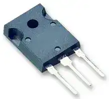


IRG4PC30FDPBF
IGBT, Fast CoPACK, N-CH, 31 A, 1.99 V, 100 W, 600 V, TO-247AC, 3 Pins
- Manufacturer: INFINEON
- Product type: Single IGBTs
- No. of Pins: 3Pins
- Power Dissipation: 100W
- Transistor Mounting: Through Hole
- Transistor Case Style: TO-247AC
- Operating Temperature Max: 150°C
- Continuous Collector Current: 31A
- Collector Emitter Voltage Max: 600V
- Collector Emitter Saturation Voltage: 1.99V
| Delivery and price | |
|---|---|
| Units per pack | 100 |
| Price | 2.44 € |
| Current stock | 10+ |
| Lead time | 30 days |
## **Features**

**==> picture [62 x 96] intentionally omitted <==**

**----- Start of picture text -----**<br>
C<br>G<br>E<br>n-channel<br>**----- End of picture text -----**<br>


**==> picture [39 x 7] intentionally omitted <==**

**----- Start of picture text -----**<br>
TO-247AC<br>**----- End of picture text -----**<br>


θ θ θ θ

www.irf.com

1

**==> picture [426 x 351] intentionally omitted <==**

**----- Start of picture text -----**<br>
[Verces ∆ ∆ _ | Collector-o-EmitterParameter Breakdown Voages| Min.600 ||——|-—Typ. |Max. | UnitsV_| Vor Conditions<br>[VcE(on)Verces Tu Temperature Coeff of Breakdown Voltage [—— [0.69 | — [WC | Vee== OV,OV, c=Ic = T.0mA250,<br>| | Collector-to-Emitter Saturation Voltage |Sic  ——- | 1.59 | 1.8 | Ic Ic = =17A 31A Voe See Fig. = 15V 2, 5<br>[Vee | —- |1.70 | — | Ic = 17A, Ty = 150°C<br>∆ ∆<br>Veet, Tu] Temperature Coeff. of Threshold Voltage| — | -11 | —— mVi°C| Voe = Vee, lo = 250uA<br>fae | Forward Transconductance © | 6.1. | 10 [—-| S| Voe=100V, lo= 17A<br>IcEs Zero Gate Voltage Collector Current |ee)—- | —- [2500 | Voe = OV, V ce e = 60 0V,0V Ty = 150°C<br>F Vem | Diode Gate Threshold Forward Voltage Vottage Drop [3.0}— [ 14/17]——[60| Vv | | Ic=12A Voe= Vers= See Fig. 13<br>|— | 1.3 | 1.6 | Ic = 12A, Ty = 150°C<br>Ices Gate-to-Emitter Leakage Current ——— |——— [+100] nA Voge = +20V<br>Switching Characteristics @ Ty = 25°C (unless otherwise specified)<br>[Q, Parameter Min.| Typ. | Max.| Units Conditions<br>[Que | Total Gate Charge (turn-on) | | 51 | 77 | c= 17A<br>[Que | Gate - Emitter Charge (turn-on) | ——-[_7.9| 12] nC | Vec=400V See Fig. 8<br>[tajory) | Gate - Collector Charge (turn-on) | —-| 19 | 28 | Vor = 15V<br>ft | Turn-OnDelayTime | | 42 | —] Ty = 25°C<br>Ω<br>[taoin | RiseTime | | 26 |) ns | Ic = 17, Voc = 480V<br>ft | Turn-Off Delay Time | | 230] 350| | Voz = 15V, Ro = 23<br>[Eon | alltime | | 160 230 Energy losses include “tail and<br>Loss|<br>[Eon[Es | Tu rn-Onr-Off SS witching Loss | =~——~ || 0.63|1.30 —-— ] mJ | diode See Fig.  reverse 9, 10, recovery. 11, 18<br>[tajor) | Total Switching Loss | ——~ | 2.02 3.9 |<br>fe | Turn-On DelayTime | | 42 | —| T= 150°C, See Fig. 9, 10, 11, 18<br>Ω<br>[taoin | RiseTime | 27 | Fs | Ic = 17, Voc = 480V<br>**----- End of picture text -----**<br>


www.irf.com

2

**==> picture [434 x 489] intentionally omitted <==**

**----- Start of picture text -----**<br>
25<br>Duty cycle: 50%<br>T   = 125°CJ<br>Ty T        = 90°Csink aa<br>20 a Gate drive as specified ||<br>Turn-on losses include<br>effects of reverse recovery<br>Power Dissipation = 24W<br>| 15<br>_ 60% of rated a<br>         voltage<br>TeteEr 105 |_|UMEHIETLEaLEIhN SNOTll= ee<br>0<br>0.1 1 10 th 100<br>f, Frequency (kHz)<br>Fig. 1 - Typical Load Current vs. Frequency<br>(Load Current = Ips of fundamental)<br>1000 1000<br>rr ee ee eee eee Ppt EE TT EP<br>T  = 25°CJJ<br>100 100<br>———— pe |||<br>T  = 150°CJJ T  = 150°CJ<br>Aa A A AT<br>a) ———<br>p O Pit i yvA<br>T  = 25°CJ<br>10 10<br>V     = 15VGEGE V      = 50VCC<br>1 eldJo20us PULSE WIDTHJo20us PULSE WIDTH20us PULSE WIDTH PULSE WIDTH WIDTH A 1 ZV}Vy ft tits+ TV eseeurses PULSE WIDTHwore<br>1 10 5 6 7 8 9 10 11 12 13<br>V     , Collector-to-Emitter Voltage (V)CECE V    , Gate-to-Emitter Voltage (V)GE<br>I   , Collector-to-Emitter Current (A)CC I   , Collector-to-Emitter Current (A)C<br>**----- End of picture text -----**<br>


**==> picture [203 x 199] intentionally omitted <==**

**----- Start of picture text -----**<br>
1000<br>rr ee ee eee eee<br>T  = 25°CJJ<br>100<br>———— pe<br>T  = 150°CJJ<br>Aa<br>a)<br>p O<br>10<br>V     = 15VGEGE<br>1 eldJo20us PULSE WIDTHJo20us PULSE WIDTH20us PULSE WIDTH PULSE WIDTH WIDTH<br>1 10<br>V     , Collector-to-Emitter Voltage (V)CECE<br>I   , Collector-to-Emitter Current (A)CC<br>**----- End of picture text -----**<br>


www.irf.com

3

**==> picture [202 x 211] intentionally omitted <==**

**----- Start of picture text -----**<br>
2.5<br>&e — oF I    = 34ACC<br>|<br>2.0 pec an<br>Leer<br>I    = 17ACC<br>TELEeeeeee ee<br>1.5<br>Ree<br>I    = 8.5ACC<br>sa<br>PEEP EEE EEE EEE<br>1.0<br>-60 -40 -20 0 20 40 60 80 100 120 140 160<br>T  , Junction Temperature (°C)JJ<br>CE<br>V     , Collector-to-Emitter Voltage (V)<br>**----- End of picture text -----**<br>


**==> picture [433 x 475] intentionally omitted <==**

**----- Start of picture text -----**<br>
40 2.5<br>— I    = 34ACC<br>P P |<br>30<br>Sopp) 2.0 pec an<br>20 PN Leer<br>I    = 17ACC<br>TTP SOT EE TELEeeeeee ee<br>1.5<br>10<br>PN) Ree<br>I    = 8.5ACC<br>acne sa<br>0 EN 1.0 PEEP EEE EEE EEE<br>25 50 75 100 125 150 -60 -40 -20 0 20 40 60 80 100 120 140<br>T   , Case Temperature (°C)C T  , Junction Temperature (°C)JJ<br>Fig. 4 - Maximum Collector Current vs. Case Fig. 5 - Typical Collector-to-Emitter Voltage<br>Temperature vs. Junction Temperature<br>10<br>po ep eppy<br>TT<br>|<br>1<br>eeesess:<br>D = 0.50<br>es<br>0.20<br>S 0.10 anYes ee PDM<br>0.1 n e etl |<br>0.05 t<br>1<br>= 0.020.01 ee       SINGLE PULSE ee ma t2<br>orm od (THERMAL RESPONSE) ee ees ee re a eee<br>e e eee eee 1. Duty factor D =  t   / t  Notes: 1 2 |<br>a ee ee<br>0.01<br>0.00001 0.0001 0.001 0.01 0.1 1 10<br>t   , Rectangular Pulse Duration (sec)1<br>Maximum DC Collector Current (A) CE<br>V     , Collector-to-Emitter Voltage (V)<br>thJC<br>Thermal Response (Z        )<br>**----- End of picture text -----**<br>


www.irf.com

4

**==> picture [207 x 196] intentionally omitted <==**

**----- Start of picture text -----**<br>
2000<br>1600 leeee<br>| NET TTT<br>s<br>1200 ee |<br>Ko TA<br>800<br>PNT PE ETT<br>es<br>400 lll<br>s<br>~IN<br>0 ell<br>1 10 100<br>V    , Collector-to-Emitter Voltage (V)CE<br>C, Capacitance (pF)<br>**----- End of picture text -----**<br>


**==> picture [197 x 198] intentionally omitted <==**

**----- Start of picture text -----**<br>
20<br>16 pote<br>Pot tt|<br>12 Po<br>Pity PA<br>8<br>pot te |<br>4 Poe<br>0 peti tf |  ft}<br>0 10 20 30 40 50 60<br>Q  , Total Gate Charge (nC)g<br>GE<br>V     , Gate-to-Emitter Voltage (V)<br>**----- End of picture text -----**<br>


**==> picture [421 x 202] intentionally omitted <==**

**----- Start of picture text -----**<br>
2.20 er 10 EREEEEREREs<br>fF loec poo ee e I    = 34AC<br>2.10 fl ret fo tg = P T<br>- is Ppp pepe pep pp pete |<br>I    = 17AC<br>| | FT] ee e<br>2.00 a im) 1 I    = 8.5AC<br>toobetoy f t<br>| || ; Fanaa ea a)=2B enEREe BP.eeeea 28 eee eee e eee<br>1.90 Pm} FP ae Oeeee<br>as EEE ET TE TEtity<br> R      = 23 G Ω<br> V      = 15VGE<br>1.80 a ee A 0.1 A  V      = 480VCC<br>0 20 40 60 80 -60 -40 -20 0 20 40 60 80 100 120 140 160<br>R   , Gate Resistance (G   Ω ) T  , Junction Temperature (°C)J<br>**----- End of picture text -----**<br>


www.irf.com

5

**==> picture [433 x 522] intentionally omitted <==**

**----- Start of picture text -----**<br>
8.0 1000<br>OT = 150°C 1 = 125°CU Hy<br>= / es<br>apse 6.0 | VY | E ee<br>100<br>oa A ee)<br>a 4.0 EDeee<br>= ee<br>| P| PY fd 10 eyA ee |<br>a |<br>2.0 If} - ALM<br>isc | | 4 vA an| ||| || 2etSEa ——eet|ee eetee See<br>0.0 i A 1 PTI ee PETee<br>0 10 20 30 40 1 10 100 1000<br>I   , Collector-to-Emitter Current (A)C V     , Collector-to-Emitter Voltage (V)CE<br>Fig. 11 - Typical Switching Losses vs. Fig. 12 - Turn-Off SOA<br>Collector-to-Emitter Current<br>100 a<br>aen ee ee ee ee<br>Pot ft eeTt ee eee ee<br>Hf | | ty<br>Pf ft<br>tL LA<br>T  = 150°CJ<br>ff<br>10 T  = 125°CJ<br>es Al7<br>= T  =   25°CJ 7<br>pot | | EAA<br>ene<br>PthE<br>LL<br>1<br>0.4 0.8 1.2 1.6 2.0 2.4<br> Forward Voltage Drop - V      (V)FM<br>C<br>I   , Collector-to-Emitter Current (A)<br>F<br>Instantaneous Forward Current - I    (A)<br>**----- End of picture text -----**<br>


www.irf.com

6

**==> picture [432 x 529] intentionally omitted <==**

**----- Start of picture text -----**<br>
160 100<br>V  = 200VR V  = 200VR<br>ees T  = 125°CJ T  = 125°CJ<br>T  = 25°CJ | T  = 25°C i J eee<br>Obps |(SeesfT fT TT TT<br>120<br>SCHJ es ee<br>wt I   = 24AF «RE<br>| LLL I   = 24AF LTT<br>I   = 12AF<br>80 * pe [a] >s 4 nl ee 10 I   = 12AF Ss betes gs<br>I   = 6.0AF<br>I   = 6.0AF<br>ealWainer |t g<br>40 rm a  SarakeSenabseia aBE aoe<br>SS 4 = QZ | |||||<br>_ |__| DQ<br>0 en ee 1<br>100 1000 100 1000<br>di  /dt - (A/µs)f di  /dt - (A/µs)f<br>Fig. 14 - Typical Reverse Recovery vs. di;/dt Fig. 15 - Typical Recovery Current vs. di;/dt<br>600 | 10000 SS<br>V  = 200VR r— V  = 200VR pp<br>T  = 125°CJ | T  = 125°CJ Pp | TT [Tt]<br>T  = 25°CJ | T  = 25°CJ Pe<br>400 Zz 1000 eee eee<br>I   = 6.0AF<br>|Ee o ee arae<br>| Tf  T e<br>; a Se<br>I   = 24AF<br>NY a -ameeeel<br>I   = 12AF<br>I   = 12AF > | Ze SS<br>200 oil 100 Z a<br>“or ne I   = 24AF e<br>I   = 6.0AF<br>ZO TU —s es<br>ZI eo )<br>0 10<br>100 1000 100 1000<br>Ser di  /dt - (A/µs)f § = EHtt di  /dt - (A/µs)f<br>t    -  (ns)rr I         - (A)IRRM<br>RR<br>Q       -  (nC)<br>di(rec)M/dt  -  (A/µs)<br>**----- End of picture text -----**<br>


www.irf.com

7

**==> picture [407 x 468] intentionally omitted <==**

**----- Start of picture text -----**<br>
90% Vge<br>+Vge<br>Same typedevice as Vce<br>D.U.T.<br>90% Ic<br>10% Vce<br>Ic<br>Ic<br>80% 430µF 5% Ic<br>of Vce D.U.T.<br>td(off) tf<br>t1+5µS<br>Eoff =  Vce ic dt<br>t1<br>Fig. 18a - Test Circuit for Measurement of fx<br>Eon: Eottidiode): ters Qrrs Irrs ta(on); tr tayote), te <—_—————_+!<br>t1 t2<br>Fig. 18b - Test Waveforms for Circuit of Fig. 18a,<br>Fost, taotry, t<br>trr<br>GATE VOLTAGE D.U.T. trr Qrr =  id dt<br>Ic<br>tx<br>10% +Vg<br>+Vg<br>tx<br>10% Irr<br>10% Vcc<br>Vcc<br>DUT VOLTAGE<br>Vce<br>AND CURRENT Vpk<br>Irr<br>Vcc [[10% Ic]] 90% Ic Ipk<br>Ic<br>DIODE RECOVERY<br>WAVEFORMS<br>PANG td(on) tr 5% Vce _— peeeeceeeeeeeereereece<br>t2<br>Eon = Vce ie dt t4<br>t1 Erec = Vd id dt<br>t3<br>t1 t2 DIODE REVERSE<br>RECOVERY ENERGY<br>t3 t4<br>∫<br>∫<br>∫<br>∫<br>**----- End of picture text -----**<br>


**==> picture [186 x 164] intentionally omitted <==**

**----- Start of picture text -----**<br>
GATE VOLTAGE D.U.T.<br>10% +Vg<br>+Vg<br>DUT VOLTAGE<br>Vce<br>AND CURRENT<br>Vcc [[10% Ic]] 90% Ic Ipk<br>Ic<br>PANG td(on) tr 5% Vce<br>t2<br>Eon = Vce ie dt<br>t1<br>t1 t2<br>∫<br>**----- End of picture text -----**<br>


www.irf.com

8

**==> picture [191 x 176] intentionally omitted <==**

**----- Start of picture text -----**<br>
Vg GATE SIGNAL<br>DEVICE UNDER TEST<br>CURRENT D.U.T.<br>VOLTAGE IN D.U.T.<br>CURRENT IN D1<br>t0 t1 t2<br>**----- End of picture text -----**<br>


Figure 18e.

**==> picture [204 x 50] intentionally omitted <==**

**----- Start of picture text -----**<br>
L D.U.T.<br>1000V V *c<br>50V<br>6000µF<br> 100V<br>**----- End of picture text -----**<br>


Figure 19.

Figure 20.

www.irf.com

9

## Notes:

**==> picture [10 x 7] intentionally omitted <==**

**----- Start of picture text -----**<br>
Ω<br>**----- End of picture text -----**<br>


≤ ≤

**==> picture [267 x 63] intentionally omitted <==**

**----- Start of picture text -----**<br>
EXAMPLE: THIS IS AN IRFPE30<br>WITH ASSEMBLY  PART NUMBER<br>LOT CODE 5657 INTERNATIONAL yO |<br>ASSEMBLED ON WW 35, 2000 RECTIFIER IRFPE30<br>IN THE ASSEMBLY LINE "H" Note:   "P" in assembly line LOGO . IQR 56           57 035H DATE CODE<br>position indicates "Lead-Free" ASSEMBLY YEAR 0 =  2000<br>LOT CODE WEEK 35<br>LINE H<br>**----- End of picture text -----**<br>


**IR WORLD HEADQUARTERS:** 233 Kansas St., El Segundo, California 90245, USA Tel: (310) 252-7105

TAC Fax: (310) 252-7903 Visit us at www.irf.com for sales contact information **.** _Data and specifications subject to change without notice._ 07/04

www.irf.com

10

Note:  For the most current drawings please refer to the IR website at: http://www.irf.com/package/
Updated at February 9, 2023
Infineon Technologies is a globally recognized leader in semiconductor solutions, renowned for driving innovation in power management, energy efficiency, and modern mobility. With a strong legacy of engineering excellence, the company provides highly reliable components designed to meet the rigorous demands of industrial, automotive, and advanced commercial applications. The core of our Infineon portfolio is centered on their industry-leading discrete semiconductors. We offer an extensive selection of single and dual MOSFETs, alongside a robust range of single IGBTs and advanced IGBT modules. These flagship power transistors are essential for high-efficiency power conversion and motor control, providing engineers with superior thermal performance and minimized switching losses. Beyond advanced field-effect transistors, the selection includes a comprehensive array of diodes and rectifiers, heavily featuring Schottky diodes, as well as fast-recovery and RF/PIN diodes. This power foundation is further supported by bipolar transistors, intelligent power modules, and thyristor SCR modules, delivering the critical building blocks required for complex power system designs. To support broader system integration, the portfolio also encompasses specialized solutions such as solid-state relays, AC/DC LED driver ICs, and Bluetooth communications modules. From high-power industrial rectifiers to wireless connectivity adapters, Infineon equips designers with the precision components needed to build efficient, scalable, and fully connected electronic systems.
About Novapart
Novapart is a B2B electronic component broker specialising in stock shortages and cost reduction. We source hard-to-find parts and identify compliant alternatives across a catalogue of 410,000+ components from 500+ manufacturers.
Learn more →Stock Shortage Specialist
When a component is unavailable, discontinued or has an unacceptable lead time, we tap into our network of vetted European and Asian distributors to source what you need — without compromising on quality or traceability.
Request a quote →Compliant Alternatives
We identify pin-to-pin, electrically equivalent substitutes that meet the same certifications (RoHS, AEC-Q100, REACH) as your original specification — validated against datasheets, not just part numbers. Often at a lower cost.
BOM Analysis service →