


IRFR9020TRPBF
Power MOSFET, P Channel, 50 V, 9.9 A, 0.28 ohm, TO-252AA, Surface Mount
- Manufacturer: VISHAY
- Product type: Single MOSFETs
- Transistor Polarity:P Channel; Continuous Drain Current Id:-9.9A; Drain Source Voltage Vds:-50V; On Resistance Rds(on):0.2ohm; Rds(on) Test Voltage Vgs:-10V; Threshold Voltage Vgs:-4V
- MSL: MSL 1 - Unlimited
- SVHC: Lead (25-Jun-2025)
- No. of Pins: 3Pins
- Channel Type: P Channel
- Product Range: -
- Qualification: -
- Power Dissipation: 42W
- Transistor Mounting: Surface Mount
- Rds(on) Test Voltage: 10V
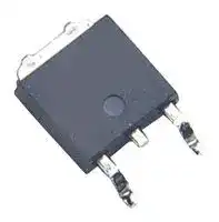
- Transistor Case Style: TO-252AA
- Drain Source Voltage Vds: 50V
- Operating Temperature Max: 150°C
- Continuous Drain Current Id: 9.9A
- Drain Source On State Resistance: 0.28ohm
- Gate Source Threshold Voltage Max: 4V
| Delivery and price | |
|---|---|
| Units per pack | 5000 |
| Price | 0.756 € |
| Current stock | 200+ |
| Lead time | 30 days |
**IRFR9020, IRFU9020, SiHFR9020, SiHFU9020** Vishay Siliconix www.vishay.com ## **Power MOSFET** **==> picture [212 x 110] intentionally omitted <==** **----- Start of picture text -----**<br> S<br>DPAK IPAK<br>(TO-252) (TO-251) G<br>D<br>D<br>S<br>G G [D] [S] D<br>P-Channel MOSFET<br>**----- End of picture text -----**<br> ## **FEATURES** - Surface mountable (order as IRFR9020, SiHFR9020) - Straight lead option (order as IRFU9020, SiHFU9020) - Repetitive avalanche ratings - Dynamic dV/dt rating - Simple drive requirements - Ease of paralleling Available - Material categorization: for definitions of compliance please see www.vishay.com/doc?99912 |**PRODUCT SUMMARY**|**PRODUCT SUMMARY**|**PRODUCT SUMMARY**| |---|---|---| |VDS(V)|-50|| |RDS(on)(Ω)|VGS= -10 V|0.28| |Qgmax. (nC)|14|| |Qgs(nC)|6.5|| |Qgd(nC)|6.5|| |Configuration|Single|| ## **DESCRIPTION** The power MOSFET technology is the key to Vishay’s advanced line of power MOSFET transistors. The efficient geometry and unique processing of this latest “State of the Art” design achieves: very low on-state resistance combined with high transconductance; superior reverse energy and diode recovery dV/dt. The power MOSFET transistors also feature all of the well established advantages of MOSFET’S such as voltage control, very fast switching, ease of paralleling and temperature stability of the electrical parameters. Surface-mount packages enhance circuit performance by reducing stray inductances and capacitance. The TO-252 surface mount package brings the advantages of power MOSFET’s to high volume applications where PC board surface mounting is desirable. The surface-mount option IRFR9020, SiHFR9020 is provided on 16mm tape. The straight lead option IRFU9020, SiHFU9020 of the device is called the IPAK (TO-251). They are well suited for applications where limited heat dissipation is required such as, computers and peripherals, telecommunication equipment, DC/DC converters, and a wide range of consumer products. |**ORDERING INFORMATION**|**ORDERING INFORMATION**|**ORDERING INFORMATION**|**ORDERING INFORMATION**|**ORDERING INFORMATION**| |---|---|---|---|---| |**PACKAGE**|**DPAK (TO-252)**|**DPAK (TO-252)**|**DPAK (TO-252)**|**IPAK (TO-251)**| |Lead (Pb)-free and halogen-free|SiHFR9020-GE3|SiHFR9020TR-GE3a|SiHFR9020TRL-GE3a|SiHFU9020-GE3| ||IRFR9020TRLPBF-BE3ab|-|-|-| |Lead (Pb)-free|IRFR9020PbF|IRFR9020TRPbFa|IRFR9020TRLPbFa|IRFU9020PbF| ## **Notes** a. See device orientation b. “-BE3” denotes alternate manufacturing location S21-0771-Rev. E, 19-Jul-2021 Document Number: 90350 **1** For technical questions, contact: hvm@vishay.com THIS DOCUMENT IS SUBJECT TO CHANGE WITHOUT NOTICE. THE PRODUCTS DESCRIBED HEREIN AND THIS DOCUMENT ARE SUBJECT TO SPECIFIC DISCLAIMERS, SET FORTH AT www.vishay.com/doc?91000 ## **IRFR9020, IRFU9020, SiHFR9020, SiHFU9020** www.vishay.com Vishay Siliconix |**ABSOLUTE MAXIMUM RATINGS**(TC= 25 °C,unless otherwise noted)|**ABSOLUTE MAXIMUM RATINGS**(TC= 25 °C,unless otherwise noted)|**ABSOLUTE MAXIMUM RATINGS**(TC= 25 °C,unless otherwise noted)|**ABSOLUTE MAXIMUM RATINGS**(TC= 25 °C,unless otherwise noted)||| |---|---|---|---|---|---| |**PARAMETER**|||**SYMBOL**|**LIMIT**|**UNIT**| |Drain-source voltage|||VDS|-50|V| |Gate-source voltage|||VGS|± 20|| |Continuous drain current|VGSat -10 V|TC= 25 °C|ID|-9.9|A| |||TC= 100 °C||-6.3|| |Pulsed drain currenta|||IDM|-40|| |Linear deratingfactor||||0.33|W/°C| |Single pulse avalanche energyb|||EAS|250|mJ| |Repetitive avalanche currenta|||IAR|-9.9|A| |Repetitive avalanche energya|||EAR|4.2|mJ| |Maximum power dissipation|TC=|25 °C|PD|42|W| |Peak diode recovery dV/dtc|||dV/dt|5.8|V/ns| |Operatingjunction and storage temperature range|||TJ, Tstg|-55 to +150|°C| |Solderingrecommendations (peak temperature)d|for|10 s||300|| ## **Notes** a. Repetitive rating; pulse width limited by maximum junction temperature (see fig. 16) b. VDD = -25 V, starting TJ = 25 °C, L = 5.1 mH, Rg = 25 Ω, peak IL = -9.9 A c. ISD ≤ -9.9 A, dI/dt ≤ -120 A/μs, VDD ≤ 40 V, TJ ≤ 150 °C d. 0.063" (1.6 mm) from case e. When mounted on 1" square PCB (FR-4 or G-10 material) |**THERMAL RESISTANCE RATINGS**|**THERMAL RESISTANCE RATINGS**|**THERMAL RESISTANCE RATINGS**|**THERMAL RESISTANCE RATINGS**|**THERMAL RESISTANCE RATINGS**|**THERMAL RESISTANCE RATINGS**| |---|---|---|---|---|---| |**PARAMETER**|**SYMBOL**|**MIN.**|**TYP.**|**MAX.**|**UNIT**| |Maximum junction-to-ambient|RthJA|-|-|110|°C/W| |Case-to-sink|RthCS|-|1.7|-|| |Maximum junction-to-case (drain)|RthJC|-|-|3.0|| |**SPECIFICATIONS**(TJ= 25 °C, unless otherwise noted)|**SPECIFICATIONS**(TJ= 25 °C, unless otherwise noted)|**SPECIFICATIONS**(TJ= 25 °C, unless otherwise noted)|**SPECIFICATIONS**(TJ= 25 °C, unless otherwise noted)||||| |---|---|---|---|---|---|---|---| |**PARAMETER**|**SYMBOL**|**TEST CONDITIONS**||**MIN.**|**TYP.**|**MAX.**|**UNIT**| |**Static**|||||||| |Drain-source breakdown voltage|VDS|VGS= 0 V, ID= -250 μA||- 50|-|-|V| |Gate-source threshold voltage|VGS(th)|VDS= VGS, ID= -50 μA||- 2.0|-|- 4.0|V| |Gate-source leakage|IGSS|VGS= ±20 V||-|-|± 500|nA| |Zero gate voltage drain current|IDSS|VDS= max. rating, VGS= 0 V||-|-|250|μA| |||VDS= 0.8 x max. rating, VGS= 0 V, TJ= 125 °C||-|-|1000|| |Drain-source on-state resistance|RDS(on)|VGS= -10 V|ID= 5.7 Ab|-|0.20|0.28|Ω| |Forward transconductance|gfs|VDS ≤-50 V, IDS= - 5.7 A||2.3|3.5|-|S| |**Dynamic**|||||||| |Input capacitance|Ciss|VGS= 0 V,<br>VDS= - 25 V,<br>f = 1.0 MHz, see fig. 9||-|490|-|pF| |Output capacitance|Coss|||-|320|-|| |Reverse transfer capacitance|Crss|||-|70|-|| |Totalgate charge|Qg|VGS= -10 V|ID= -9.7 A, VDS= 0.8 x max.<br>rating, see fig. 18 (Independent<br>operating temperature)|-|9.4|14|nC| |Gate-source charge|Qgs|||-|4.3|6.5|| |Gate-drain charge|Qgd|||-|4.3|6.5|| |Turn-on delay time|td(on)|VDD= -25 V, ID= -9.7 A,<br>Rg= 18Ω, RD= 2.4Ω, see fig. 17<br>(Independent operating temperature)||-|8.2|12|ns| |Rise time|tr|||-|57|66|| |Turn-off delay time|td(off)|||-|12|18|| |Fall time|tf|||-|25|38|| |Internal drain inductance|LD|Between lead, 6 mm (0.25")<br>from package and center of<br>die contact.<br>D<br>S<br>G||-|4.5|-|nH| |Internal source inductance|LS|||-|7.5|-|| S21-0771-Rev. E, 19-Jul-2021 Document Number: 90350 **2** For technical questions, contact: hvm@vishay.com THIS DOCUMENT IS SUBJECT TO CHANGE WITHOUT NOTICE. THE PRODUCTS DESCRIBED HEREIN AND THIS DOCUMENT ARE SUBJECT TO SPECIFIC DISCLAIMERS, SET FORTH AT www.vishay.com/doc?91000 **==> picture [77 x 24] intentionally omitted <==** **----- Start of picture text -----**<br> —<br>www.vishay.com<br>**----- End of picture text -----**<br> ## **IRFR9020, IRFU9020, SiHFR9020, SiHFU9020** ## Vishay Siliconix ## **SPECIFICATIONS** (TJ = 25 °C, unless otherwise noted) |**SPECIFICATIONS**(TJ = 25 °C, unless otherwise noted)TJ = 25 °C, unless otherwise noted)J = 25 °C, unless otherwise noted)= 25 °C, unless otherwise noted), unless otherwise noted)unless otherwise noted))|**SPECIFICATIONS**(TJ = 25 °C, unless otherwise noted)TJ = 25 °C, unless otherwise noted)J = 25 °C, unless otherwise noted)= 25 °C, unless otherwise noted), unless otherwise noted)unless otherwise noted))|**SPECIFICATIONS**(TJ = 25 °C, unless otherwise noted)TJ = 25 °C, unless otherwise noted)J = 25 °C, unless otherwise noted)= 25 °C, unless otherwise noted), unless otherwise noted)unless otherwise noted))|**SPECIFICATIONS**(TJ = 25 °C, unless otherwise noted)TJ = 25 °C, unless otherwise noted)J = 25 °C, unless otherwise noted)= 25 °C, unless otherwise noted), unless otherwise noted)unless otherwise noted))|**SPECIFICATIONS**(TJ = 25 °C, unless otherwise noted)TJ = 25 °C, unless otherwise noted)J = 25 °C, unless otherwise noted)= 25 °C, unless otherwise noted), unless otherwise noted)unless otherwise noted))|**SPECIFICATIONS**(TJ = 25 °C, unless otherwise noted)TJ = 25 °C, unless otherwise noted)J = 25 °C, unless otherwise noted)= 25 °C, unless otherwise noted), unless otherwise noted)unless otherwise noted))|**SPECIFICATIONS**(TJ = 25 °C, unless otherwise noted)TJ = 25 °C, unless otherwise noted)J = 25 °C, unless otherwise noted)= 25 °C, unless otherwise noted), unless otherwise noted)unless otherwise noted))| |---|---|---|---|---|---|---| |**PARAMETER**|**SYMBOL**|**TEST CONDITIONS**|**MIN.**|**TYP.**|**MAX.**|**UNIT**| |**Drain-source body diode characteristics**||||||| |Continuous source-drain diode current|IS|MOSFET symbol<br>showing the integral reverse<br>p - n junction diode<br>S<br>D<br>G|-|-|-9.9|A| |Pulsed diode forward currenta|ISM||-|-|- 40|| |Body diode voltage|VSD|TJ= 25 °C, IS= - 9.9 A, VGS= 0 Vb|-|-|- 6.3|V| |Body diode reverse recovery time|trr|TJ= 25 °C, IF= - 9,7 A, dI/dt = 100 A/μsb|56|110|280|ns| |Body diode reverse recovery charge|Qrr||0.17|0.34|0.85|nC| |Forward turn-on time|ton|Intrinsic turn-on time is negligible (turn-on is dominated by LSand LD)||||| ## **Notes** a. Repetitive rating; pulse width limited by maximum junction temperature (see fig. 16) b. Pulse width ≤ 300 μs; duty cycle ≤ 2 % ## **TYPICAL CHARACTERISTICS** (25 °C, unless otherwise noted) **Fig. 1 - Typical Output Characteristics** **Fig. 3 - Typical Saturation Characteristics** **==> picture [156 x 9] intentionally omitted <==** **----- Start of picture text -----**<br> Fig. 2 - Typical Transfer Characteristics<br>**----- End of picture text -----**<br> **==> picture [148 x 9] intentionally omitted <==** **----- Start of picture text -----**<br> Fig. 4 - Maximum Safe Operating Area<br>**----- End of picture text -----**<br> S21-0771-Rev. E, 19-Jul-2021 Document Number: 90350 **3** For technical questions, contact: hvm@vishay.com THIS DOCUMENT IS SUBJECT TO CHANGE WITHOUT NOTICE. THE PRODUCTS DESCRIBED HEREIN AND THIS DOCUMENT ARE SUBJECT TO SPECIFIC DISCLAIMERS, SET FORTH AT www.vishay.com/doc?91000 ## www.vishay.com ## **IRFR9020** ~~a~~ **, IRFU9020, SiHFR9020, SiHFU9020** Vishay Siliconix **Fig. 5 - Typical Transconductance vs. Drain Current** **Fig. 8 - Breakdown Voltage vs. Temperature** **Fig. 6 - Typical Source-Drain Diode Forward Voltage** **Fig. 9 - Typical Capacitance vs. Drain-to-Source Voltage** **Fig. 7 - Breakdown Voltage vs. Temperature** **Fig. 10 - Typical Gate Charge vs. Gate-to-Source Voltage** Document Number: 90350 S21-0771-Rev. E, 19-Jul-2021 **4** For technical questions, contact: hvm@vishay.com THIS DOCUMENT IS SUBJECT TO CHANGE WITHOUT NOTICE. THE PRODUCTS DESCRIBED HEREIN AND THIS DOCUMENT ARE SUBJECT TO SPECIFIC DISCLAIMERS, SET FORTH AT www.vishay.com/doc?91000 **IRFR9020, IRFU9020, SiHFR9020, SiHFU9020** ## www.vishay.com **Fig. 11 - Typical On-Resistance vs. Drain Current** ## Vishay Siliconix **Fig. 14 - Unclamped Inductive Test Circuit** **==> picture [139 x 94] intentionally omitted <==** **----- Start of picture text -----**<br> IAS -—- —_—-<br>\ |fo<br>VDS \ IL | f<br>NO]<br>MLN<br>VDD<br>k— tp ><br>\<br>VDS<br>**----- End of picture text -----**<br> **Fig. 12 - Maximum Drain Current vs. Case Temperature** **Fig. 15 - Unclamped Inductive Waveforms** **Fig. 13 - Maximum Avalanche vs. Starting Junction Temperature** Document Number: 90350 S21-0771-Rev. E, 19-Jul-2021 **5** For technical questions, contact: hvm@vishay.com THIS DOCUMENT IS SUBJECT TO CHANGE WITHOUT NOTICE. THE PRODUCTS DESCRIBED HEREIN AND THIS DOCUMENT ARE SUBJECT TO SPECIFIC DISCLAIMERS, SET FORTH AT www.vishay.com/doc?91000 **IRFR9020, IRFU9020, SiHFR9020, SiHFU9020** www.vishay.com Vishay Siliconix Fig. 16 - Maximum Effective Transient Thermal Impedance, Junction-to-Case vs. Pulse Duration **==> picture [340 x 108] intentionally omitted <==** **----- Start of picture text -----**<br> td(on) tr td(off) tf<br>VGS ! | 1 QG<br>10 % - 10 V<br>Via<br>QGS QGD<br>90 %VDS X\__/ VG<br>Charge<br>**----- End of picture text -----**<br> **Fig. 17 - Switching Time Waveforms** **Fig. 19 - Basic Gate Charge Waveform** **Fig. 18 - Switching Time Test Circuit** **Fig. 20 - Gate Charge Test Circuit** Document Number: 90350 S21-0771-Rev. E, 19-Jul-2021 **6** For technical questions, contact: hvm@vishay.com THIS DOCUMENT IS SUBJECT TO CHANGE WITHOUT NOTICE. THE PRODUCTS DESCRIBED HEREIN AND THIS DOCUMENT ARE SUBJECT TO SPECIFIC DISCLAIMERS, SET FORTH AT www.vishay.com/doc?91000 **IRFR9020, IRFU9020, SiHFR9020, SiHFU9020** Vishay Siliconix **==> picture [77 x 10] intentionally omitted <==** **----- Start of picture text -----**<br> www.vishay.com<br>**----- End of picture text -----**<br> ## **Peak Diode Recovery dV/dt Test Circuit** **==> picture [258 x 231] intentionally omitted <==** **----- Start of picture text -----**<br> D.U.T.<br>+<br>Circuit layout considerations<br>• Low stray inductance<br>• Ground plane<br>• Low leakage inductance<br>current transformer<br>-<br>+<br>-<br>Rg • dV/dt controlled by Rg +<br>• • ID.U.T. - device under testSD controlled by duty factor “D” - VDD<br>Note<br>• Compliment N-Channel of D.U.T. for driver<br>- +<br>**----- End of picture text -----**<br> **==> picture [284 x 230] intentionally omitted <==** **----- Start of picture text -----**<br> Driver gate drive<br>P.W.<br>Period D =<br>P.W. Period<br>VGS = - 10 V [a]<br>D.U.T. lSD waveform<br>Reverse<br>recovery Body diode forward<br>current current<br>dI/dt<br>D.U.T. VDS waveform<br>Diode recovery<br>dV/dt<br>VDD<br>Re-applied<br>voltage<br>Body diode forward drop<br>Inductor current<br>Ripple ≤ 5 % ISD<br>Note<br>a. VGS = - 5 V for logic level and - 3 V drive devices<br>**----- End of picture text -----**<br> **==> picture [90 x 9] intentionally omitted <==** **----- Start of picture text -----**<br> Fig. 21 - For P-Channel<br>**----- End of picture text -----**<br> _Vishay Siliconix maintains worldwide manufacturing capability. Products may be manufactured at one of several qualified locations. Reliability data for Silicon Technology and Package Reliability represent a composite of all qualified locations. For related documents such as package/tape drawings, part marking, and reliability data, see www.vishay.com/ppg?90350._ S21-0771-Rev. E, 19-Jul-2021 Document Number: 90350 **7** For technical questions, contact: hvm@vishay.com THIS DOCUMENT IS SUBJECT TO CHANGE WITHOUT NOTICE. THE PRODUCTS DESCRIBED HEREIN AND THIS DOCUMENT ARE SUBJECT TO SPECIFIC DISCLAIMERS, SET FORTH AT www.vishay.com/doc?91000 **Package Information** Vishay Siliconix **==> picture [59 x 48] intentionally omitted <==** www.vishay.com ## **TO-252AA Case Outline** ## **VERSION 1: FACILITY CODE = Y** **==> picture [364 x 211] intentionally omitted <==** **----- Start of picture text -----**<br> E A<br>C2<br>b3<br>E1<br>b b2 C<br>e<br>A1<br>e1<br>L3<br>D1<br>D<br>H<br>L4<br>L5 L<br>gage plane height (0.5 mm)<br>**----- End of picture text -----**<br> |b|b2<br>e1<br>gage plane height (0.5 mm)<br>e|b2<br>e1<br>gage plane height (0.5 mm)<br>e| |---|---|---| ||**MILLIMETERS**|| |**DIM.**|**MIN.**|**MAX.**| |A|2.18|2.38| |A1|-|0.127| |b|0.64|0.88| |b2|0.76|1.14| |b3|4.95|5.46| |C|0.46|0.61| |C2|0.46|0.89| |D|5.97|6.22| |D1|4.10|-| |E|6.35|6.73| |E1|4.32|-| |H|9.40|10.41| |e|2.28 BSC|| |e1|4.56 BSC|| |L|1.40|1.78| |L3|0.89|1.27| |L4|-|1.02| |L5|1.01|1.52| ## **Note** - Dimension L3 is for reference only Revision: 16-Dec-2019 Document Number: 71197 **1** For technical questions, contact: pmostechsupport@vishay.com THIS DOCUMENT IS SUBJECT TO CHANGE WITHOUT NOTICE. THE PRODUCTS DESCRIBED HEREIN AND THIS DOCUMENT ARE SUBJECT TO SPECIFIC DISCLAIMERS, SET FORTH AT www.vishay.com/doc?91000 **Package Information** Vishay Siliconix **==> picture [59 x 48] intentionally omitted <==** www.vishay.com ## **VERSION 2: FACILITY CODE = N** **==> picture [338 x 254] intentionally omitted <==** **----- Start of picture text -----**<br> e<br>E A<br>b3<br>E1<br>e c2 E1/2<br>2x b2<br>2x e 3x b 0.25 C A B DETAIL "B" (b)<br>H<br>C<br>b1<br>GAUGE<br>PLANE SEATING DETAIL "B"<br>C C<br>L PLANE<br>(L1)<br>(3°) (3°)<br>θ<br>θ<br>L3 D1<br>D<br>H<br>L6<br>L5<br>L4<br>c<br>c1<br>L2 A1<br>θ<br>**----- End of picture text -----**<br> ||**MILLIMETERS**|**MILLIMETERS**| |---|---|---| |**DIM.**|**MIN.**|**MAX.**| |A|2.18|2.39| |A1|-|0.13| |b|0.65|0.89| |b1|0.64|0.79| |b2|0.76|1.13| |b3|4.95|5.46| |c|0.46|0.61| |c1|0.41|0.56| |c2|0.46|0.60| |D|5.97|6.22| |D1|5.21|-| |E|6.35|6.73| |E1|4.32|-| |e|2.29 BSC|| |H|9.94|10.34| ||**MILLIMETERS**|**MILLIMETERS**| |---|---|---| |**DIM.**|**MIN.**|**MAX.**| |L|1.50|1.78| |L1|2.74 ref.|| |L2|0.51 BSC|| |L3|0.89|1.27| |L4|-|1.02| |L5|1.14|1.49| |L6|0.65|0.85| ||0°|10°| |1|0°|15°| |2|25°|35°| ## **Notes** - Dimensioning and tolerance confirm to ASME Y14.5M-1994 - All dimensions are in millimeters. Angles are in degrees - Heat sink side flash is max. 0.8 mm - Radius on terminal is optional ECN: E19-0649-Rev. Q, 16-Dec-2019 DWG: 5347 Revision: 16-Dec-2019 Document Number: 71197 **2** For technical questions, contact: pmostechsupport@vishay.com THIS DOCUMENT IS SUBJECT TO CHANGE WITHOUT NOTICE. THE PRODUCTS DESCRIBED HEREIN AND THIS DOCUMENT ARE SUBJECT TO SPECIFIC DISCLAIMERS, SET FORTH AT www.vishay.com/doc?91000 **Package Information** Vishay Siliconix www.vishay.com ## **Case Outline for TO-251AA (High Voltage)** ## **OPTION 1:** **==> picture [378 x 278] intentionally omitted <==** **----- Start of picture text -----**<br> 4 3 A<br>E1 Thermal PAD E A<br>4<br>b4 0.010 0.25 M C A B c2<br>L2 4 A<br>θ2 θ1<br>D1 4<br>B<br>C<br>3<br>Seating<br>5 plane<br>L1 L3 C C<br>(Datum A)<br>L<br>B B<br>A<br>A1<br>3 x b2<br>c<br>3 x b<br>View A - A 2 x e 0.010 0.25 M C A B<br>Base<br>5 metal<br>Plating<br>b1, b3<br>Lead tip<br>(c) c1 5<br>( b, b2)<br>Section B - B and C - C<br>D<br>**----- End of picture text -----**<br> ||**MILLIMETERS**|**MILLIMETERS**|**INCHES**|**INCHES**||**MILLIMETERS**<br>**INCHES**<br>**DIM.**<br>**MIN.**<br>**MAX.**<br>**MIN.**<br>**MAX.**<br>D1<br>5.21<br>-<br>0.205<br>-<br>E<br>6.35<br>6.73<br>0.250<br>0.265<br>E1<br>4.32<br>-<br>0.170<br>-<br>e<br>2.29 BSC<br>2.29 BSC<br>L<br>8.89<br>9.65<br>0.350<br>0.380<br>L1<br>1.91<br>2.29<br>0.075<br>0.090<br>L2<br>0.89<br>1.27<br>0.035<br>0.050<br>L3<br>1.14<br>1.52<br>0.045<br>0.060<br>θ1<br>0'<br>15'<br>0'<br>15'<br>θ2<br>25'<br>35'<br>25'<br>35'|**MILLIMETERS**|**MILLIMETERS**|**INCHES**|**INCHES**| |---|---|---|---|---|---|---|---|---|---|---| |**DIM.**|**MIN.**|**MAX.**|**MIN.**|**MAX.**|||**MIN.**|**MAX.**|**MIN.**|**MAX.**| |A|2.18|2.39|0.086|0.094|||5.21|-|0.205|-| |A1|0.89|1.14|0.035|0.045|||6.35|6.73|0.250|0.265| |b|0.64|0.89|0.025|0.035|||4.32|-|0.170|-| |b1|0.65|0.79|0.026|0.031|||2.29 BSC||2.29 BSC|| |b2|0.76|1.14|0.030|0.045|||8.89|9.65|0.350|0.380| |b3|0.76|1.04|0.030|0.041|||1.91|2.29|0.075|0.090| |b4|4.95|5.46|0.195|0.215|||0.89|1.27|0.035|0.050| |c|0.46|0.61|0.018|0.024|||1.14|1.52|0.045|0.060| |c1|0.41|0.56|0.016|0.022|||0'|15'|0'|15'| |c2|0.46|0.86|0.018|0.034|||25'|35'|25'|35'| |D|5.97|6.22|0.235|0.245||||||| |ECN: E21-0605-Rev. B, 25-Oct-2021<br>DWG: 5968||||||||||| |||||||||||| ## **Notes** - Dimensioning and tolerancing per ASME Y14.5M-1994 - Dimension are shown in inches and millimeters - Dimension D and E do not include mold flash. Mold flash shall not exceed 0.13 mm (0.005") per side. These dimensions are measured at the outermost extremes of the plastic body - Thermal pad contour optional with dimensions b4, L2, E1 and D1 - Lead dimension uncontrolled in L3 - Dimension b1, b3 and c1 apply to base metal only - Outline conforms to JEDEC[®] outline TO-251AA Revision: 25-Oct-2021 Document Number: 91362 **1** For technical questions, contact: hvmos.techsupport@vishay.com THIS DOCUMENT IS SUBJECT TO CHANGE WITHOUT NOTICE. THE PRODUCTS DESCRIBED HEREIN AND THIS DOCUMENT ARE SUBJECT TO SPECIFIC DISCLAIMERS, SET FORTH AT www.vishay.com/doc?91000 **Package Information** Vishay Siliconix **==> picture [77 x 10] intentionally omitted <==** **----- Start of picture text -----**<br> www.vishay.com<br>**----- End of picture text -----**<br> ## **OPTION 2: FACILITY CODE = N** |Ø 1.00<br>x 0.10 deep<br>L2<br>L4<br>L3|Ø 1.00<br>x 0.10 deep<br>L2<br>L4<br>L3|L2||E<br>b4<br>CL|E<br>b4<br>CL|E<br>b4<br>CL||D<br>L1<br>C<br>B<br>L|θ1<br><br>θ1|θ1<br><br>θ1|θ1<br><br>θ1|||A1<br>D1<br>Third angle<br>projection|||||||c1<br>D2|c1<br>D2|c1<br>D2| |---|---|---|---|---|---|---|---|---|---|---|---|---|---|---|---|---|---|---|---|---|---|---|---| ||||||||||||||||||||||||| |||||||||||θ1||c|A<br>2|A1|||||||||| ||||||||||||||||D1||E1||||||| ||||||||||||||||||||||||| |||||||||||||||||||||||D2|| |||||||||||θ1|||||||||||||| ||||||||||||||||||||||||| ||||||||||||||||||||||||| |||L4|||||||||||||||||||||| |||||b2<br>b<br>e<br>C<br>B|||||||||||||||||||| |||L3|||||||||||||||||||||| ||||||||||||||||||||||||| ||||||||||||||||||||||||| ||||||||||||||c|||c|b1, b3<br>b, b2<br><br>Section “B-B” a|||nd “C-C”|||| ||||||e||||||||||||||||||| |||||||||θ2|||||||||||||||| ||||||||||||||||||||||||| ||||||||||||||||||||||||| ||||||||||||||||||||||||| |**DIM.**|||**MIN.**|||**MAX.**||**MAX.**||||||**DIM.**|||**MIN.**|||**MAX.**|||**MAX.**| |A|||2.180|||2.285||2.390||||||D2|||5.380|||-|||-| |A1|||0.890|||1.015||1.140||||||E|||6.350|||6.540|||6.730| |b|||0.640|||0.765||0.890||||||E1|||4.32|||-|||-| |b1|||0.640|||0.715||0.790||||||e|||2.29 BSC||||||| |b2|||0.760|||0.950||1.140||||||L|||8.890||9.270||||9.650| |b3|||0.760|||0.900||1.040||||||L1|||1.910||2.100||||2.290| |b4|||4.950|||5.205||5.460||||||L2|||0.890||1.080||||1.270| |c|||0.460|||-||0.610||||||L3|||1.140||1.330||||1.520| |c1|||0.410|||-||0.560||||||L4|||1.300||1.400||||1.500| |c2|||0.460|||-||0.610||||||θ1|||0°||7.5°||||15°| |D|||5.970|||6.095||6.220||||||θ2|||4°||-||||-| |D1|||4.300|||-||-|||||||||||||||| |ECN: E21-0605-Rev. B, 25-Oct-2021<br>DWG: 5968|||||||||||||||||||||||| ||||||||||||||||||||||||| ## **Notes** - Dimensioning and tolerancing per ASME Y14.5M-1994 - All dimension are in millimeters, angles are in degrees - Heat sink side flash is max. 0.8 mm Revision: 25-Oct-2021 Document Number: 91362 **2** For technical questions, contact: hvmos.techsupport@vishay.com THIS DOCUMENT IS SUBJECT TO CHANGE WITHOUT NOTICE. THE PRODUCTS DESCRIBED HEREIN AND THIS DOCUMENT ARE SUBJECT TO SPECIFIC DISCLAIMERS, SET FORTH AT www.vishay.com/doc?91000 **Application Note 826** **==> picture [60 x 50] intentionally omitted <==** ## Vishay Siliconix ## **RECOMMENDED MINIMUM PADS FOR DPAK (TO-252)** **==> picture [203 x 287] intentionally omitted <==** **----- Start of picture text -----**<br> 0.224<br>(5.690)<br>0.180 0.055<br>(4.572) (1.397)<br>0.243 (6.180)<br>0.420<br>(10.668)<br>0.087 (2.202)<br>0.090 (2.286)<br>**----- End of picture text -----**<br> Recommended Minimum Pads Dimensions in Inches/(mm) > Return to Index Return to Index Document Number: 72594 Revision: 21-Jan-08 www.vishay.com 3 **Legal Disclaimer Notice** Vishay www.vishay.com ## **Disclaimer** ALL PRODUCT, PRODUCT SPECIFICATIONS AND DATA ARE SUBJECT TO CHANGE WITHOUT NOTICE TO IMPROVE RELIABILITY, FUNCTION OR DESIGN OR OTHERWISE. Vishay Intertechnology, Inc., its affiliates, agents, and employees, and all persons acting on its or their behalf (collectively, “Vishay”), disclaim any and all liability for any errors, inaccuracies or incompleteness contained in any datasheet or in any other disclosure relating to any product. Vishay makes no warranty, representation or guarantee regarding the suitability of the products for any particular purpose or the continuing production of any product. To the maximum extent permitted by applicable law, Vishay disclaims (i) any and all liability arising out of the application or use of any product, (ii) any and all liability, including without limitation special, consequential or incidental damages, and (iii) any and all implied warranties, including warranties of fitness for particular purpose, non-infringement and merchantability. Statements regarding the suitability of products for certain types of applications are based on Vishay's knowledge of typical requirements that are often placed on Vishay products in generic applications. Such statements are not binding statements about the suitability of products for a particular application. It is the customer's responsibility to validate that a particular product with the properties described in the product specification is suitable for use in a particular application. Parameters provided in datasheets and / or specifications may vary in different applications and performance may vary over time. All operating parameters, including typical parameters, must be validated for each customer application by the customer's technical experts. Product specifications do not expand or otherwise modify Vishay's terms and conditions of purchase, including but not limited to the warranty expressed therein. Hyperlinks included in this datasheet may direct users to third-party websites. These links are provided as a convenience and for informational purposes only. Inclusion of these hyperlinks does not constitute an endorsement or an approval by Vishay of any of the products, services or opinions of the corporation, organization or individual associated with the third-party website. Vishay disclaims any and all liability and bears no responsibility for the accuracy, legality or content of the third-party website or for that of subsequent links. Except as expressly indicated in writing, Vishay products are not designed for use in medical, life-saving, or life-sustaining applications or for any other application in which the failure of the Vishay product could result in personal injury or death. Customers using or selling Vishay products not expressly indicated for use in such applications do so at their own risk. Please contact authorized Vishay personnel to obtain written terms and conditions regarding products designed for such applications. No license, express or implied, by estoppel or otherwise, to any intellectual property rights is granted by this document or by any conduct of Vishay. Product names and markings noted herein may be trademarks of their respective owners. _**© 2021 VISHAY INTERTECHNOLOGY, INC. ALL RIGHTS RESERVED**_ Revision: 09-Jul-2021 Document Number: 91000 **1**
Updated at April 29, 2026
Vishay is a global leader in the manufacturing of discrete semiconductors and passive electronic components. Renowned for its exceptional quality and engineering expertise, the company produces highly reliable solutions that drive innovation across the industrial, automotive, telecommunications, and consumer electronics markets. From advanced factory automation to vehicle electrification, Vishay components provide the foundational building blocks for modern electronic design. The company's expansive portfolio is heavily focused on efficient power management, signal routing, and energy storage. Within its passive component lineup, Vishay is recognized for its extensive array of high-performance capacitors, including robust aluminium electrolytic, film, and polymer variants, alongside highly efficient power inductors. In the realm of discrete semiconductors, Vishay is a premier manufacturer of single and dual MOSFETs, as well as a vast selection of Schottky, Zener, and fast-recovery rectifier diodes designed for demanding power applications. Furthermore, Vishay delivers industry-leading circuit protection and thermal management solutions. With a broad offering of transient voltage suppressors (TVS diodes) and temperature-sensing NTC thermistors, these components are engineered to safeguard sensitive circuitry against both electrical and thermal overstress. By combining this vital mix of advanced discretes and passives, Vishay enables engineers to develop robust, space-saving, and highly resilient electronic systems.
About Novapart
Novapart is a B2B electronic component broker specialising in stock shortages and cost reduction. We source hard-to-find parts and identify compliant alternatives across a catalogue of 410,000+ components from 500+ manufacturers.
Learn more →Stock Shortage Specialist
When a component is unavailable, discontinued or has an unacceptable lead time, we tap into our network of vetted European and Asian distributors to source what you need — without compromising on quality or traceability.
Request a quote →Compliant Alternatives
We identify pin-to-pin, electrically equivalent substitutes that meet the same certifications (RoHS, AEC-Q100, REACH) as your original specification — validated against datasheets, not just part numbers. Often at a lower cost.
BOM Analysis service →