
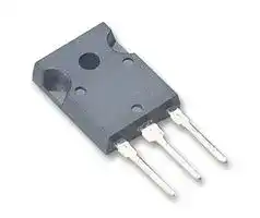


IRFPS43N50KPBF
Power MOSFET, N Channel, 500 V, 47 A, 0.078 ohm, TO-274AA, Through Hole
- Manufacturer: VISHAY
- Product type: Single MOSFETs
- No. of Pins: 3Pins
- Channel Type: N Channel
- Power Dissipation: 540W
- Transistor Mounting: Through Hole
- Transistor Polarity: N Channel
- Power Dissipation Pd: 540W
- Rds(on) Test Voltage: 10V
- On Resistance Rds(on): 0.078ohm
- Transistor Case Style: TO-274AA
- Drain Source Voltage Vds: 500V
- Operating Temperature Max: 150°C
- Continuous Drain Current Id: 47A
- Drain Source On State Resistance: 0.078ohm
- Gate Source Threshold Voltage Max: 5V
| Delivery and price | |
|---|---|
| Units per pack | 1 |
| Price | 12.14 € |
| Current stock | 10+ |
| Lead time | 30 days |
**IRFPS43N50K, SiHFPS43N50K** Vishay Siliconix ## **Power MOSFET** ## **FEATURES** **PRODUCT SUMMARY** VDS (V) 500 • Low Gate Charge Qg Results in Simple Drive Requirement Available RDS(on) ( ) VGS = 10 V 0.078 QQgg (Max.) (nC)s (nC) 35085 • Improved Gate, Avalanche and Dynamic dV/dtRuggedness **RoHS*COMPLIANT** Qgd (nC) 180 • Fully Characterized Capacitance and Avalanche Voltage ~~a~~ Configuration Single and Current : D • Low RDS(on) • Compliant to RoHS Directive 2002/95/EC **Super-247 APPLICATIONS** G • Switch Mode Power Supply (SMPS) S D • Uninterruptible Power Supply ee G S • High Speed Power Switching N-Channel MOSFET • Hard Switched and High Frequency Circuits - Hard Switched and High Frequency Circuits **ORDERING INFORMATION** Package Super-247 IRFPS43N50KPbF Lead (Pb)-free SiHFPS43N50K-E3 IRFPS43N50K SnPb SiHFPS43N50K ~~——S~~ **ABSOLUTE MAXIMUM RATINGS** (TC = 25 °C, unless otherwise noted) **PARAMETER SYMBOL LIMIT UNIT** Drain-Source Voltage VDS 500 V Gate-Source Voltage VGS ± 30 TC = 25 °C 47 Continuous Drain Current VGS at 10 V ID TC = 100 °C 29 A Pulsed Drain Current[a] IDM 190 Linear Derating Factor 4.3 W/°C Single Pulse Avalanche Energy[b] EAS 910 mJ Repetitive Avalanche Current[a] IAR 47 A Repetitive Avalanche Energy[a] EAR 54 mJ Maximum Power Dissipation TC = 25 °C PD 540 W Peak Diode Recovery dV/dt[c] dV/dt 9.0 V/ns Operating Junction and Storage Temperature Range TJ, Tstg - 55 to + 150 °C ~~TT~~ Soldering Recommendations (Peak Temperature) for 10 s 300[d] **Notes** a. Repetitive rating; pulse width limited by maximum junction temperature (see fig. 11). b. Starting TJ = 25 °C, L = 0.82 mH, Rg = 25 , IAS = 47 A (see fig. 12c). - c. ISD 47 A, dI/dt 230 A/μs, VDD VDS, TJ 150 °C. - d. 1.6 mm from case. * Pb containing terminations are not RoHS compliant, exemptions may apply Document Number: 91262 S11-0112-Rev. C, 31-Jan-11 www.vishay.com 1 **IRFPS43N50K, SiHFPS43N50K** Vishay Siliconix **==> picture [59 x 48] intentionally omitted <==** ## **THERMAL RESISTANCE RATINGS** |**THERMAL RESISTANCE RATINGS**|**THERMAL RESISTANCE RATINGS**|**THERMAL RESISTANCE RATINGS**|**THERMAL RESISTANCE RATINGS**|**THERMAL RESISTANCE RATINGS**| |---|---|---|---|---| |**PARAMETER**|**SYMBOL**|**TYP.**|**MAX.**|**UNIT**| |Maximum Junction-to-Ambient|RthJA|-|40|°C/W| |Case-to-Sink, Flat, Greased Surface|RthCS|0.24|-|| |Maximum Junction-to-Case (Drain)|RthJC|-|0.23|| |**SPECIFICATIONS**(TJ= 25 °C,unless otherwise noted)|**SPECIFICATIONS**(TJ= 25 °C,unless otherwise noted)|**SPECIFICATIONS**(TJ= 25 °C,unless otherwise noted)|**SPECIFICATIONS**(TJ= 25 °C,unless otherwise noted)||||| |---|---|---|---|---|---|---|---| |**PARAMETER**|**SYMBOL**|**TEST CONDITIONS**||**MIN.**|**TYP.**|**MAX.**|**UNIT**| |**Static**|||||||| |Drain-Source Breakdown Voltage|VDS|VGS= 0 V, ID= 250 μA||500|-|-|V| |VDSTemperature Coefficient|VDS/TJ|Reference to 25 °C, ID= 1 mA||-|0.60|-|V/°C| |Gate-Source Threshold Voltage|VGS(th)|VDS= VGS, ID= 250 μA||3.0|-|5.0|V| |Gate-Source Leakage|IGSS|VGS= ± 30 V||-|-|± 100|nA| |Zero Gate Voltage Drain Current|IDSS|VDS= 500 V, VGS= 0 V||-|-|50|μA| |||VDS= 400 V, VGS= 0 V, TJ= 125 °C||-|-|250|| |Drain-Source On-State Resistance|RDS(on)|VGS= 10 V|ID= 28 Ab|-|0.078|0.090|| |Forward Transconductance|gfs|VDS= 50 V, ID= 28 A||23|-|-|S| |**Dynamic**|||||||| |Input Capacitance|Ciss|VGS= 0 V,<br>VDS= 25 V,<br>f = 1.0 MHz, see fig. 5||-|8310|-|pF| |Output Capacitance|Coss|||-|960|-|| |Reverse Transfer Capacitance|Crss|||-|120|-|| |Output Capacitance|Coss|VGS= 0 V|VDS= 1.0 V, f = 1.0 MHz|-|10170|-|| ||||VDS= 400 V, f = 1.0 MHz|-|240|-|| |Effective Output Capacitance|Cosseff.||VDS= 0 V to 400 Vc|-|440|-|| |Total Gate Charge|Qg|VGS= 10 V|ID= 47 A, VDS= 400 V,<br>see fig. 6 and 13b|-|-|350|nC| |Gate-Source Charge|Qgs|||-|-|85|| |Gate-Drain Charge|Qgd|||-|-|180|| |Turn-On Delay Time|td(on)||VDD= 250 V, ID= 47 A,<br>RG= 1.0, see fig. 10b|-|25|-|ns| |Rise Time|tr|||-|140|-|| |Turn-Off Delay Time|td(off)|||-|55|-|| |Fall Time|tf|||-|74|-|| |**Drain-Source Body Diode Characteristics**|||||||| |Continuous Source-Drain Diode Current|IS|MOSFET symbol<br>showing the<br>integral reverse<br>p - n junction diode<br>S<br>D<br>G||-|-|47|A| |Pulsed Diode Forward Currenta|ISM|||-|-|190|| |Body Diode Voltage|VSD|TJ= 25 °C, IS= 47 A, VGS= 0 Vb||-|-|1.5|V| |Body Diode Reverse Recovery Time|trr|TJ= 25 °C, IF= 47 A, dI/dt = 100 A/μsb||-|620|940|ns| |Body Diode Reverse Recovery Charge|Qrr|||-|14|21|μC| |Body Diode Recovery Current|IRRM|||-|38|-|A| |Forward Turn-On Time|ton|Intrinsic turn-on time is negligible (turn-on is dominated by LSand LD)|||||| ## **Notes** a. Repetitive rating; pulse width limited by maximum junction temperature (see fig. 11). b. Pulse width 400 μs; duty cycle 2 %. c. Coss eff. is a fixed capacitance that gives the same charging time as Coss while VDS is rising from 0 % to 80 % VDS. www.vishay.com 2 Document Number: 91262 S11-0112-Rev. C, 31-Jan-11 **IRFPS43N50K, SiHFPS43N50K** Vishay Siliconix **==> picture [59 x 48] intentionally omitted <==** ## **TYPICAL CHARACTERISTICS** (25 °C, unless otherwise noted) **==> picture [206 x 199] intentionally omitted <==** **----- Start of picture text -----**<br> 1000<br>VGS<br>TOP 15V<br>10V<br>8.0V<br>7.0V<br> 100 6.0V<br>5.5V<br>5.0V<br>BOTTOM4.5V<br> 10<br> 1<br>4.5V<br>0.1<br>20µs PULSE WIDTH T = 25J °C<br>0.01<br>0.1 1 10 100<br>V , Drain-to-Source Voltage (V)DS<br>D<br>I , Drain-to-Source Current (A)<br>**----- End of picture text -----**<br> **Fig. 1 - Typical Output Characteristics** **==> picture [226 x 211] intentionally omitted <==** **----- Start of picture text -----**<br> 1000<br> 100 T = 150 CJ °<br> 10<br>T = 25 C J °<br> 1<br>V = 50VDS<br>20µs PULSE WIDTH<br>0.1<br>4 5 6 7 8 9 10 11 12<br>V , Gate-to-Source Voltage (V)GS<br>Fig. 3 - Typical Transfer Characteristics<br>D<br>I , Drain-to-Source Current (A)<br>**----- End of picture text -----**<br> **==> picture [209 x 211] intentionally omitted <==** **----- Start of picture text -----**<br> 1000<br>VGS<br>TOP 15V<br>10V<br>8.0V<br>7.0V<br>6.0V<br>5.5V<br> 100 5.0V<br>BOTTOM4.5V<br> 10<br>4.5V<br> 1<br>20µs PULSE WIDTH T = 150J °C<br>0.1<br>0.1 1 10 100<br>V , Drain-to-Source Voltage (V)DS<br>Fig. 2 - Typical Output Characteristics<br>D<br>I , Drain-to-Source Current (A)<br>**----- End of picture text -----**<br> **==> picture [225 x 200] intentionally omitted <==** **----- Start of picture text -----**<br> 3.5<br>ID = 48A<br>3.0<br>2.5<br>2.0<br>1.5<br>1.0<br>0.5<br>VGS= 10V<br>0.0<br>-60 -40 -20 0 20 40 60 80 100 120 140 160<br>T , Junction TemperatureJ ( C)°<br>(Normalized)<br>DS(on)<br>R , Drain-to-Source On Resistance<br>**----- End of picture text -----**<br> **Fig. 4 - Normalized On-Resistance vs. Temperature** Document Number: 91262 S11-0112-Rev. C, 31-Jan-11 www.vishay.com 3 **IRFPS43N50K, SiHFPS43N50K** ## Vishay Siliconix **==> picture [214 x 194] intentionally omitted <==** **----- Start of picture text -----**<br> 1000000<br>VGS = 0V, f = 1 MHZ<br>Ciss = Cgs + Cgd, Cds SHORTED<br>100000 Crss = Cgd<br>C = C + C<br>oss ds gd<br>10000 Ciss<br>1000<br>Coss<br>100<br>Crss<br>10<br>1 10 100 1000<br>VDS, Drain-to-Source Voltage (V)<br>C, Capacitance(pF)<br>**----- End of picture text -----**<br> **Fig. 5 - Typical Capacitance vs. Drain-to-Source Voltage** **==> picture [217 x 200] intentionally omitted <==** **----- Start of picture text -----**<br> 20<br>ID = 48A<br>VDS= 400V<br>VDS= 250V<br>VDS= 100V<br>15<br>10<br>5<br>0<br>0 50 100 150 200 250 300 350<br>Q , Total Gate Charge (nC)G<br>GS<br>V , Gate-to-Source Voltage (V)<br>**----- End of picture text -----**<br> **Fig. 6 - Typical Gate Charge vs. Gate-to-Source Voltage** **==> picture [59 x 48] intentionally omitted <==** **==> picture [219 x 468] intentionally omitted <==** **----- Start of picture text -----**<br> 1000<br> 100<br>T = 150 CJ °<br> 10<br>T = 25 C J °<br> 1<br>V = 0 V GS<br>0.1<br>0.2 0.7 1.2 1.7 2.2<br>V ,Source-to-Drain Voltage (V)SD<br>Fig. 7 - Typical Source-Drain Diode Forward Voltage<br> 1000<br>OPERATION IN THIS AREA LIMITED<br>BY RDS(on)<br> 100 10us<br>100us<br> 10<br>1ms<br> T T CJ = 25 C = 150 C ° ° 10ms<br> Single Pulse<br> 1<br> 10 100 1000<br>V , Drain-to-Source Voltage (V)DS<br>I , Reverse Drain Current (A)SD<br>I , Drain Current (A) D<br>**----- End of picture text -----**<br> **Fig. 7 - Typical Source-Drain Diode Forward Voltage** **Fig. 8 - Maximum Safe Operating Area** www.vishay.com 4 Document Number: 91262 S11-0112-Rev. C, 31-Jan-11 **IRFPS43N50K, SiHFPS43N50K** **==> picture [59 x 48] intentionally omitted <==** ## Vishay Siliconix **==> picture [225 x 208] intentionally omitted <==** **----- Start of picture text -----**<br> 50<br>40<br>30<br>20<br>10<br>0<br>25 50 75 100 125 150<br>T , Case TemperatureC ( C)°<br>I , Drain Current (A)D<br>**----- End of picture text -----**<br> **Fig. 9 - Maximum Drain Current vs. Case Temperature** **==> picture [152 x 219] intentionally omitted <==** **----- Start of picture text -----**<br> RD<br>VDS<br>VGS<br>D.U.T.<br>RG +- VDD<br>10 V<br>Pulse width ≤ 1 µs<br>Duty factor ≤ 0.1 %<br>Fig. 10a - Switching Time Test Circuit<br>VDS<br>90 %<br>10 %<br>VGS<br>td(on) tr td(off) tf<br>**----- End of picture text -----**<br> **Fig. 10b - Switching Time Waveforms** **==> picture [486 x 207] intentionally omitted <==** **----- Start of picture text -----**<br> 1<br>D = 0.50<br>0.1<br>0.20<br>0.10<br>0.05 PDM<br>0.01 0.020.01 SINGLE PULSE t1<br>(THERMAL RESPONSE) t2<br>Notes:<br>1. Duty factor D = t / t1 2<br>2. Peak TJ = P DM x ZthJC + TC<br>0.001<br>0.00001 0.0001 0.001 0.01 0.1 1<br>t , Rectangular Pulse Duration (sec)1<br>thJC<br>(Z )<br>Thermal Response<br>**----- End of picture text -----**<br> **Fig. 11 - Maximum Effective Transient Thermal Impedance, Junction-to-Case** Document Number: 91262 S11-0112-Rev. C, 31-Jan-11 www.vishay.com 5 **IRFPS43N50K, SiHFPS43N50K** Vishay Siliconix **==> picture [59 x 48] intentionally omitted <==** **==> picture [418 x 134] intentionally omitted <==** **----- Start of picture text -----**<br> 15 V VDS<br>t<br>p<br>L Driver<br>VDS<br>RG D.U.T +<br>- [V][DD] A<br>20 V IAS IAS<br>tp 0.01 Ω<br>**----- End of picture text -----**<br> **Fig. 12a - Unclamped Inductive Test Circuit** **Fig. 12b - Unclamped Inductive Waveforms** **==> picture [228 x 203] intentionally omitted <==** **----- Start of picture text -----**<br> 2000<br>ID<br>TOP 22A<br>30A<br>BOTTOM 47A<br>1500<br>1000<br>500<br>0<br>25 50 75 100 125 150<br>Starting T , Junction TemperatureJ ( C)°<br>AS<br>E , Single Pulse Avalanche Energy (mJ)<br>**----- End of picture text -----**<br> **Fig. 12c - Maximum Avalanche Energy vs. Drain Current** **==> picture [415 x 148] intentionally omitted <==** **----- Start of picture text -----**<br> Current regulator<br>Same type as D.U.T.<br>QG 50 kΩ<br>10 V 12 V 0.2 µF<br>0.3 µF<br>QGS QGD +<br>D.U.T. - VDS<br>VG VGS<br>3 mA<br>Charge<br>IG ID<br>Current sampling resistors<br>**----- End of picture text -----**<br> **Fig. 13a - Basic Gate Charge Waveform** **Fig. 13b - Gate Charge Test Circuit** www.vishay.com 6 Document Number: 91262 S11-0112-Rev. C, 31-Jan-11 **IRFPS43N50K, SiHFPS43N50K** Vishay Siliconix **==> picture [59 x 48] intentionally omitted <==** **==> picture [286 x 494] intentionally omitted <==** **----- Start of picture text -----**<br> Peak Diode Recovery dV/dt Test Circuit<br>+ Circuit layout considerations<br>D.U.T.<br>• Low stray inductance<br>• Ground plane<br>• Low leakage inductance<br>current transformer<br>-<br>+<br>- - +<br>Rg • dV/dt controlled by Rg +<br>•• Driver same type as D.U.T.ISD controlled by duty factor “D” - VDD<br>• D.U.T. - device under test<br>Driver gate drive<br>Period D = P.W.<br>P.W. Period<br>VGS = 10 V [a]<br>D.U.T. lSD waveform<br>Reverse<br>recovery Body diode forward<br>current current dI/dt<br>D.U.T. VDS waveform Diode recovery<br>dV/dt<br>VDD<br>Re-applied<br>voltage<br>Body diode forward drop<br>Inductor current<br>Ripple ≤ 5 % ISD<br>Note<br>a. VGS = 5 V for logic level devices<br>**----- End of picture text -----**<br> **Fig. 14 - For N-Channel** _Vishay Siliconix maintains worldwide manufacturing capability. Products may be manufactured at one of several qualified locations. Reliability data for Silicon Technology and Package Reliability represent a composite of all qualified locations. For related documents such as package/tape drawings, part marking, and reliability data, see www.vishay.com/ppg?91262._ Document Number: 91262 S11-0112-Rev. C, 31-Jan-11 www.vishay.com 7 **Package Information** **==> picture [60 x 50] intentionally omitted <==** ## Vishay Siliconix ## **TO-274AA (HIGH VOLTAGE)** **==> picture [470 x 359] intentionally omitted <==** **----- Start of picture text -----**<br> A<br>B E A<br>D2<br>E4 A1 E1<br>R<br>D1<br>D<br>L1<br>L Detail “A”<br>C<br>e b<br>A2<br>0.10 (0.25) M B A M<br>b2 b4<br>Lead Tip<br>Detail “A”<br>Scale: 2:1<br>10°<br>5°<br>**----- End of picture text -----**<br> ||**MILLIMETERS**|**MILLIMETERS**|**INCHES**|**INCHES**|||**MILLIMETERS**|**MILLIMETERS**|**INCHES**|**INCHES**| |---|---|---|---|---|---|---|---|---|---|---| |**DIM.**|**MIN.**<br>|**MAX.**|**MIN.**|**MAX.**||**DIM.**|**MIN.**|**MAX.**|**MIN.**|**MAX.**| |A|4.70|5.30|0.185|0.209||D1|15.50|16.10|0.610|0.634| |A1|1.50|2.50|0.059|0.098||D2|0.70|1.30|0.028|0.051| |A2|2.25|2.65|0.089|0.104||E|15.10|16.10|0.594|0.634| |b|1.30|1.60|0.051|0.063||E1|13.30|13.90|0.524|0.547| |b2|1.80|2.20|0.071|0.087||e|5.45 BSC||0.215 BSC|| |b4|3.00|3.25|0.118|0.128||L|13.70|14.70|0.539|0.579| |c|0.80|1.20|0.031|0.047||L1|1.00|1.60|0.039|0.063| |D|19.80<br>|20.80|0.780|0.819||R|2.00|3.00|0.079|0.118| |ECN: S-82247-Rev. A, 06-Oct-08<br>DWG:5975||||||||||| ECN: S-82247-Rev. A, 06-Oct-08 DWG: 5975 ## **Notes** 1. Dimensioning and tolerancing per ASME Y14.5M-1994. 2. Dimension D and E do not include mold flash. Mold flash shall not exceed 0.127 mm (0.005") per side. These dimensions are measured at the outer extremes of the plastic body. 3. Outline conforms to JEDEC outline to TO-274AA. Document Number: 91365 Revision: 06-Oct-08 www.vishay.com 1 **Legal Disclaimer Notice** Vishay www.vishay.com **==> picture [59 x 48] intentionally omitted <==** ## **Disclaimer** ALL PRODUCT, PRODUCT SPECIFICATIONS AND DATA ARE SUBJECT TO CHANGE WITHOUT NOTICE TO IMPROVE RELIABILITY, FUNCTION OR DESIGN OR OTHERWISE. Vishay Intertechnology, Inc., its affiliates, agents, and employees, and all persons acting on its or their behalf (collectively, “Vishay”), disclaim any and all liability for any errors, inaccuracies or incompleteness contained in any datasheet or in any other disclosure relating to any product. Vishay makes no warranty, representation or guarantee regarding the suitability of the products for any particular purpose or the continuing production of any product. To the maximum extent permitted by applicable law, Vishay disclaims (i) any and all liability arising out of the application or use of any product, (ii) any and all liability, including without limitation special, consequential or incidental damages, and (iii) any and all implied warranties, including warranties of fitness for particular purpose, non-infringement and merchantability. Statements regarding the suitability of products for certain types of applications are based on Vishay’s knowledge of typical requirements that are often placed on Vishay products in generic applications. Such statements are not binding statements about the suitability of products for a particular application. It is the customer’s responsibility to validate that a particular product with the properties described in the product specification is suitable for use in a particular application. Parameters provided in datasheets and / or specifications may vary in different applications and performance may vary over time. All operating parameters, including typical parameters, must be validated for each customer application by the customer’s technical experts. Product specifications do not expand or otherwise modify Vishay’s terms and conditions of purchase, including but not limited to the warranty expressed therein. Except as expressly indicated in writing, Vishay products are not designed for use in medical, life-saving, or life-sustaining applications or for any other application in which the failure of the Vishay product could result in personal injury or death. Customers using or selling Vishay products not expressly indicated for use in such applications do so at their own risk. Please contact authorized Vishay personnel to obtain written terms and conditions regarding products designed for such applications. No license, express or implied, by estoppel or otherwise, to any intellectual property rights is granted by this document or by any conduct of Vishay. Product names and markings noted herein may be trademarks of their respective owners. Revision: 13-Jun-16 Document Number: 91000 **1**
Updated at February 9, 2023
Vishay is a global leader in the manufacturing of discrete semiconductors and passive electronic components. Renowned for its exceptional quality and engineering expertise, the company produces highly reliable solutions that drive innovation across the industrial, automotive, telecommunications, and consumer electronics markets. From advanced factory automation to vehicle electrification, Vishay components provide the foundational building blocks for modern electronic design. The company's expansive portfolio is heavily focused on efficient power management, signal routing, and energy storage. Within its passive component lineup, Vishay is recognized for its extensive array of high-performance capacitors, including robust aluminium electrolytic, film, and polymer variants, alongside highly efficient power inductors. In the realm of discrete semiconductors, Vishay is a premier manufacturer of single and dual MOSFETs, as well as a vast selection of Schottky, Zener, and fast-recovery rectifier diodes designed for demanding power applications. Furthermore, Vishay delivers industry-leading circuit protection and thermal management solutions. With a broad offering of transient voltage suppressors (TVS diodes) and temperature-sensing NTC thermistors, these components are engineered to safeguard sensitive circuitry against both electrical and thermal overstress. By combining this vital mix of advanced discretes and passives, Vishay enables engineers to develop robust, space-saving, and highly resilient electronic systems.
About Novapart
Novapart is a B2B electronic component broker specialising in stock shortages and cost reduction. We source hard-to-find parts and identify compliant alternatives across a catalogue of 410,000+ components from 500+ manufacturers.
Learn more →Stock Shortage Specialist
When a component is unavailable, discontinued or has an unacceptable lead time, we tap into our network of vetted European and Asian distributors to source what you need — without compromising on quality or traceability.
Request a quote →Compliant Alternatives
We identify pin-to-pin, electrically equivalent substitutes that meet the same certifications (RoHS, AEC-Q100, REACH) as your original specification — validated against datasheets, not just part numbers. Often at a lower cost.
BOM Analysis service →