


IRFIBE30GPBF
Power MOSFET, N Channel, 800 V, 2.1 A, 3 ohm, TO-220FP, Through Hole
- Manufacturer: VISHAY
- Product type: Single MOSFETs
- Transistor Polarity:N Channel; Continuous Drain Current Id:2.1A; Drain Source Voltage Vds:800V; On Resistance Rds(on):3ohm; Rds(on) Test Voltage Vgs:10V; Threshold Voltage Vgs:4V; Power Dissipation P
- MSL: -
- SVHC: Lead (21-Jan-2025)
- No. of Pins: 3Pins
- Channel Type: N Channel
- Product Range: -
- Qualification: -
- Power Dissipation: 35W
- Transistor Mounting: Through Hole
- Rds(on) Test Voltage: 10V
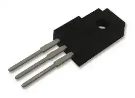
- Transistor Case Style: TO-220FP
- Drain Source Voltage Vds: 800V
- Operating Temperature Max: 150°C
- Continuous Drain Current Id: 2.1A
- Drain Source On State Resistance: 3ohm
- Gate Source Threshold Voltage Max: 4V
| Delivery and price | |
|---|---|
| Units per pack | 5000 |
| Price | 1.02 € |
| Current stock | 50+ |
| Lead time | 30 days |
**IRFIBE30G** Vishay Siliconix

www.vishay.com

## **Power MOSFET**

**==> picture [204 x 116] intentionally omitted <==**

**----- Start of picture text -----**<br>
D<br>TO-220 FULLPAK<br>G o l<br>Se<br>S S<br>D<br>G<br>N-Channel MOSFET<br>**----- End of picture text -----**<br>


## **FEATURES**

- Isolated package

- High voltage isolation = 2.5 kVRMS (t = 60 s; f = 60 Hz)

- Sink to lead creepage distance = 4.8 mm

- Dynamic dV/dt rating

- Low thermal resistance

- Material categorization: for definitions of compliance please see www.vishay.com/doc?99912

## **DESCRIPTION**

|**PRODUCT SUMMARY**|**PRODUCT SUMMARY**|**PRODUCT SUMMARY**|
|---|---|---|
|VDS(V)|800||
|RDS(on)(Ω)|VGS= 10 V|3.0|
|Qg(Max.) (nC)|78||
|Qgs(nC)|9.6||
|Qgd(nC)|45||
|Configuration|Single||


Third generation power MOSFETs from Vishay provides the designer with the best combination of fast switching, ruggedized device design, low on-resistance and cost effectiveness.

The TO-220 FULLPAK eliminates the need for additional insulating hardware in commercial-industrial applications. The molding compound used provides a high isolation capability and a low thermal resistance between the tab and external heatsink. This isolation is equivalent to using a 100 micron mica barrier with standard TO-220 product. The FULLPAK is mounted to a heatsink using a single clip or by a single screw fixing.

## **ORDERING INFORMATION**

|Package|TO-220 FULLPAK|
|---|---|
|Lead (Pb)-free|IRFIBE30GPbF|


|**ABSOLUTE MAXIMUM RATINGS**TC= 25 °C, unless otherwise noted<br>~~C~~~~**e**~~|**ABSOLUTE MAXIMUM RATINGS**TC= 25 °C, unless otherwise noted<br>~~C~~~~**e**~~|**ABSOLUTE MAXIMUM RATINGS**TC= 25 °C, unless otherwise noted<br>~~C~~~~**e**~~|**ABSOLUTE MAXIMUM RATINGS**TC= 25 °C, unless otherwise noted<br>~~C~~~~**e**~~|**ABSOLUTE MAXIMUM RATINGS**TC= 25 °C, unless otherwise noted<br>~~C~~~~**e**~~|**ABSOLUTE MAXIMUM RATINGS**TC= 25 °C, unless otherwise noted<br>~~C~~~~**e**~~|
|---|---|---|---|---|---|
|**PARAMETER**<br>~~C~~~~**e**~~<br>~~e~~<br>~~_——~~|||**SYMBOL**<br>~~e~~<br>~~_——~~|**LIMIT**<br>~~e~~<br>~~_——~~|**UNIT**<br>~~e~~<br>~~_——~~|
|Drain-source voltage<br>~~_——~~|||VDS<br>~~_——~~|800<br>~~_——~~|V<br>~~_——~~|
|Gate-source voltage<br>~~_——~~<br>~~|~~|||VGS<br>~~_——~~|± 20<br>~~_——~~<br>~~Po~~||
|Continuous drain current<br>~~_——~~<br>~~pp~~|VGSat 10 V<br>~~_——~~<br>~~|~~<br>~~pp~~|TC= 25 °C<br>~~_——~~<br>~~|~~<br>~~pp~~|ID<br>~~_——~~<br>~~pp~~|2.1<br>~~_——~~<br>~~Po~~<br>~~pp~~|A<br>~~_——~~<br>~~pp~~<br>~~a~~|
|||TC= 100 °C<br>~~|~~<br>~~pp~~||1.4<br>~~Po~~<br>~~pp~~||
|Pulsed drain currenta<br>~~pp~~<br>~~a~~|||IDM<br>~~pp~~<br>~~a~~|8.4<br>~~pp~~<br>~~a~~||
|Linear deratingfactor||||0.28|W/°C|
|Singlepulse avalanche energyb<br>~~a~~<br>~~**a**~~|||EAS<br>~~a~~<br>|240<br>~~a~~<br>|mJ<br>~~a~~<br>|
|Repetitive avalanche currenta<br>~~a~~<br>~~**a**~~|||IAR<br>~~a~~<br>|2.1<br>~~a~~<br>|A<br>~~a~~<br>|
|Repetitive avalanche energy a<br>~~**a**~~|||EAR<br>|3.5<br>|mJ<br>|
|Maximumpower dissipation<br>~~a~~|TC= 25 °C<br>~~a~~||PD<br>~~a~~|35<br>~~a~~|W<br>~~a~~|
|Peak diode recoverydV/dtc<br>~~a~~<br>~~nn~~|||dV/dt<br>~~a~~|2.0<br>~~a~~<br>~~EE~~|V/ns<br>~~a~~|
|Operating junction and storage temperature range<br>~~nn~~|||TJ,Tstg|-55 to +150<br>~~EE~~|°C|
|Solderingrecommendations(peak temperature) d<br>~~nn~~|For 10 s<br>~~nn~~|||300<br>~~EE~~||
|Mountingtorque<br>~~nn~~<br>~~a~~|M3 screw<br>~~nn~~|||0.6<br>~~EE~~|Nm|


## **Notes**

a. Repetitive rating; pulse width limited by maximum junction temperature (see fig. 11)

b. VDD = 50 V, starting TJ = 25 °C, L = 102 mH, RG = 25 Ω, IAS = 2.1 A (see fig. 12)

c. ISD ≤ 4.1 A, dI/dt ≤ 100 A/μs, VDD ≤ 600 V, TJ ≤ 150 °C

d. 1.6 mm from case

S21-0976-Rev. C, 11-Oct-2021

Document Number: 91184

**1**

For technical questions, contact: hvmos.techsupport@vishay.com THIS DOCUMENT IS SUBJECT TO CHANGE WITHOUT NOTICE. THE PRODUCTS DESCRIBED HEREIN AND THIS DOCUMENT ARE SUBJECT TO SPECIFIC DISCLAIMERS, SET FORTH AT www.vishay.com/doc?91000

**IRFIBE30G**

www.vishay.com

Vishay Siliconix

## **THERMAL RESISTANCE RATINGS**

|**THERMAL RESISTANCE RATINGS**|**THERMAL RESISTANCE RATINGS**|**THERMAL RESISTANCE RATINGS**|**THERMAL RESISTANCE RATINGS**|**THERMAL RESISTANCE RATINGS**|
|---|---|---|---|---|
|**PARAMETER**|**SYMBOL**|**TYP.**|**MAX.**|**UNIT**|
|Maximum junction-to-ambient|RthJA|-|65|°C/W|
|Maximum junction-to-case (drain)|RthJC|-|3.6||


|**SPECIFICATIONS**T**J**= 25 °C, unless otherwise noted|**SPECIFICATIONS**T**J**= 25 °C, unless otherwise noted|**SPECIFICATIONS**T**J**= 25 °C, unless otherwise noted|**SPECIFICATIONS**T**J**= 25 °C, unless otherwise noted|||||
|---|---|---|---|---|---|---|---|
|**PARAMETER**|**SYMBOL**|**TEST CONDITIONS**||**MIN.**|**TYP.**|**MAX.**|**UNIT**|
|**Static**||||||||
|Drain-ssource breakdown voltage|VDS|VGS= 0 V, ID= 250 μA||800|-|-|V|
|VDStemperature coefficient|ΔVDS/TJ|Reference to 25 °C, ID= 1 mA||-|0.90|-|V/°C|
|Gate-source threshold voltage|VGS(th)|VDS= VGS, ID= 250 μA||2.0|-|4.0|V|
|Gate-source leakage|IGSS|VGS= ± 20 V||-|-|± 100|nA|
|Zero gate voltage drain current|IDSS|VDS= 800 V, VGS= 0 V||-|-|100|μA|
|||VDS= 640 V, VGS= 0 V, TJ= 125 °C||-|-|500||
|Drain-source on-state resistance|RDS(on)|VGS= 10 V|ID= 1.3 Ab|-|-|3.0|Ω|
|Forward transconductance|gfs|VDS= 50 V, ID= 1.3 Ab||1.7|-|-|S|
|**Dynamic**||||||||
|Input capacitance|Ciss|VGS= 0 V,<br>VDS= 25 V,<br>f = 1.0 MHz, see fig. 5||-|1300|-|pF|
|Output capacitance|Coss|||-|310|-||
|Reverse transfer capacitance|Crss|||-|190|-||
|Drain to sink capacitance|C|f = 1.0 MHz||-|12|-||
|Total gate charge|Qg|VGS= 10 V|ID= 4.1 A, VDS= 400 V,<br>see fig. 6 and 13b|-|-|78|nC|
|Gate-source charge|Qgs|||-|-|9.6||
|Gate-drain charge|Qgd|||-|-|45||
|Turn-on delay time|td(on)|VDD= 400 V, ID= 4.1 A,<br>RG= 12Ω,RD= 95Ω,<br>see fig. 10b||-|12|-|ns|
|Rise time|tr|||-|33|-||
|Turn-off delay time|td(off)|||-|82|-||
|Fall time|tf|||-|30|-||
|Internal drain inductance|LD|Between lead,<br>6 mm (0.25") from<br>package and center of<br>die contact<br>D<br>S<br>G||-|4.5|-|nH|
|Internal source inductance|LS|||-|7.5|-||
|**Drain-Source Body Diode Characteristics**||||||||
|Continuous source-drain diode current|IS|MOSFET symbol<br>showing the<br>integral reverse<br>p - n junction diode<br>S<br>D<br>G||-|-|2.1|A|
|Pulsed diode forward currenta|ISM|||-|-|8.4||
|Body diode voltage|VSD|TJ= 25 °C, IS= 2.1 A, VGS= 0 Vb||-|-|1.8|V|
|Body diode reverse recovery time|trr|TJ= 25 °C, IF= 4.1 A, dI/dt = 100 A/μsb||-|480|720|ns|
|Body diode reverse recovery charge|Qrr|||-|1.8|2.7|μC|
|Forward turn-on time|ton|Intrinsic turn-on time is negligible (turn-on is dominated by LSand LD)||||||


## **Notes**

a. Repetitive rating; pulse width limited by maximum junction temperature (see fig. 11) b. Pulse width ≤ 300 μs; duty cycle ≤ 2 %

Document Number: 91184

S21-0976-Rev. C, 11-Oct-2021

**2**

For technical questions, contact: hvmos.techsupport@vishay.com THIS DOCUMENT IS SUBJECT TO CHANGE WITHOUT NOTICE. THE PRODUCTS DESCRIBED HEREIN AND THIS DOCUMENT ARE SUBJECT TO SPECIFIC DISCLAIMERS, SET FORTH AT www.vishay.com/doc?91000

**IRFIBE30G** Vishay Siliconix

## www.vishay.com

## **TYPICAL CHARACTERISTICS** 25 °C, unless otherwise noted

**Fig. 1 - Typical Output Characteristics, TC = 25 °C**

**Fig. 2 - Typical Output Characteristics, TC = 150 °C**

**Fig. 3 - Typical Transfer Characteristics**

**Fig. 4 - Normalized On-Resistance vs. Temperature**

S21-0976-Rev. C, 11-Oct-2021

Document Number: 91184

**3** For technical questions, contact: hvmos.techsupport@vishay.com THIS DOCUMENT IS SUBJECT TO CHANGE WITHOUT NOTICE. THE PRODUCTS DESCRIBED HEREIN AND THIS DOCUMENT ARE SUBJECT TO SPECIFIC DISCLAIMERS, SET FORTH AT www.vishay.com/doc?91000

**IRFIBE30G** Vishay Siliconix

## www.vishay.com

**Fig. 5 - Typical Capacitance vs. Drain-to-Source Voltage**

**Fig. 6 - Typical Gate Charge vs. Gate-to-Source Voltage**

**Fig. 7 - Typical Source-Drain Diode Forward Voltage**

**Fig. 8 - Maximum Safe Operating Area**

S21-0976-Rev. C, 11-Oct-2021

Document Number: 91184

**4** For technical questions, contact: hvmos.techsupport@vishay.com THIS DOCUMENT IS SUBJECT TO CHANGE WITHOUT NOTICE. THE PRODUCTS DESCRIBED HEREIN AND THIS DOCUMENT ARE SUBJECT TO SPECIFIC DISCLAIMERS, SET FORTH AT www.vishay.com/doc?91000

**IRFIBE30G**

**==> picture [77 x 10] intentionally omitted <==**

**----- Start of picture text -----**<br>
www.vishay.com<br>**----- End of picture text -----**<br>


## Vishay Siliconix

**==> picture [211 x 100] intentionally omitted <==**

**----- Start of picture text -----**<br>
L<br>VDS<br>Vary tp to obtain<br>required IAS<br>RG D.U.T +<br>- [V][ DD]<br>IAS<br>* 10 V<br>t p 0.01 Ω<br>**----- End of picture text -----**<br>


**==> picture [146 x 97] intentionally omitted <==**

**----- Start of picture text -----**<br>
VDS<br>t<br>~~ p —_<br>VDD<br>/<br>VDS<br>/ \<br>IAS anne<br>**----- End of picture text -----**<br>


**Fig. 9a - Unclamped Inductive Test Circuit**

**Fig. 9b - Unclamped Inductive Waveforms**

**Fig. 9c - Maximum Avalanche Energy vs. Drain Current**

**==> picture [415 x 166] intentionally omitted <==**

**----- Start of picture text -----**<br>
Current regulator<br>Same type as D.U.T.<br>QG 50 kΩ<br>VGS 12 V 0.2 µF<br>0.3 µF<br>QGS QGD +<br>D.U.T. - VDS<br>VG VGS<br>3 mA<br>: Charge |<br>IG ID<br>Current sampling resistors<br>Fig. 10a - Basic Gate Charge Waveform Fig. 10b - Gate Charge Test Circuit<br>**----- End of picture text -----**<br>


Document Number: 91184

S21-0976-Rev. C, 11-Oct-2021

**5**

For technical questions, contact: hvmos.techsupport@vishay.com THIS DOCUMENT IS SUBJECT TO CHANGE WITHOUT NOTICE. THE PRODUCTS DESCRIBED HEREIN AND THIS DOCUMENT ARE SUBJECT TO SPECIFIC DISCLAIMERS, SET FORTH AT www.vishay.com/doc?91000

**IRFIBE30G**

Vishay Siliconix

**==> picture [77 x 10] intentionally omitted <==**

**----- Start of picture text -----**<br>
www.vishay.com<br>**----- End of picture text -----**<br>


## **Peak Diode Recovery dV/dt Test Circuit**

**==> picture [284 x 463] intentionally omitted <==**

**----- Start of picture text -----**<br>
+ Circuit layout considerations<br>D.U.T.<br>•  Low stray inductance<br>•  Ground plane<br>•  Low leakage inductance<br>current transformer<br>-<br>+<br>- - +<br>Rg •  dV/dt controlled by Rg +<br>••   Driver same type as D.U.T.ISD controlled by duty factor “D” - VDD<br>•  D.U.T. - device under test<br>Driver gate drive<br>P.W.<br>Period D =<br>P.W. Period<br>VGS = 10 V [a]<br>D.U.T. lSD waveform<br>Reverse<br>recovery Body diode forward<br>current current dI/dt<br>D.U.T. VDS waveform Diode recovery<br>dV/dt<br>VDD<br>Re-applied<br>voltage<br>Body diode forward drop<br>Inductor current<br>Ripple ≤ 5 % ISD<br>Note<br>a. VGS = 5 V for logic level devices<br>**----- End of picture text -----**<br>


**Fig. 14 - For N-Channel**

_Vishay Siliconix maintains worldwide manufacturing capability. Products may be manufactured at one of several qualified locations. Reliability data for Silicon Technology and Package Reliability represent a composite of all qualified locations. For related documents such as package/tape drawings, part marking, and reliability data, see www.vishay.com/ppg?91184._

Document Number: 91184

S21-0976-Rev. C, 11-Oct-2021

**6**

For technical questions, contact: hvmos.techsupport@vishay.com THIS DOCUMENT IS SUBJECT TO CHANGE WITHOUT NOTICE. THE PRODUCTS DESCRIBED HEREIN AND THIS DOCUMENT ARE SUBJECT TO SPECIFIC DISCLAIMERS, SET FORTH AT www.vishay.com/doc?91000

**Package Information** Vishay Siliconix

**==> picture [59 x 48] intentionally omitted <==**

www.vishay.com

## **TO-220 FULLPAK (High Voltage)**

## **OPTION 1: FACILITY CODE = 9**

**==> picture [394 x 245] intentionally omitted <==**

**----- Start of picture text -----**<br>
A<br>E F<br>A3<br>3 x b2 Mold flash<br>3 x b1 bleeding  Q<br>Exposed Cu<br>3 x b<br>2 x e C Bottom view<br>Ø R<br>1<br>Q<br>G<br>D<br>L1<br>L<br>**----- End of picture text -----**<br>


||**MILLIMETERS**|**MILLIMETERS**|**MILLIMETERS**|
|---|---|---|---|
|**DIM.**|**MIN.**|**NOM.**|**MAX.**|
|A|4.60|4.70|4.80|
|b|0.70|0.80|0.91|
|b1|1.20|1.30|1.47|
|b2|1.10|1.20|1.30|
|C|0.45|0.50|0.63|
|D|15.80|15.87|15.97|
|e|2.54 BSC|||
|E|10.00|10.10|10.30|
|F|2.44|2.54|2.64|
|G|6.50|6.70|6.90|
|L|12.90|13.10|13.30|
|L1|3.13|3.23|3.33|
|Q|2.65|2.75|2.85|
|Q1|3.20|3.30|3.40|
|Ø R|3.08|3.18|3.28|


## **Notes**

1. To be used only for process drawing

2. These dimensions apply to all TO-220 FULLPAK leadframe versions 3 leads

3. All critical dimensions should C meet Cpk > 1.33

4. All dimensions include burrs and plating thickness

5. No chipping or package damage

6. Facility code will be the 1[st] character located at the 2[nd] row of the unit marking

Revision: 08-Apr-2019

Document Number: 91359

**1**

For technical questions, contact: hvmos.techsupport@vishay.com THIS DOCUMENT IS SUBJECT TO CHANGE WITHOUT NOTICE. THE PRODUCTS DESCRIBED HEREIN AND THIS DOCUMENT ARE SUBJECT TO SPECIFIC DISCLAIMERS, SET FORTH AT www.vishay.com/doc?91000

**Package Information**

Vishay Siliconix

**==> picture [59 x 48] intentionally omitted <==**

www.vishay.com

## **OPTION 2: FACILITY CODE = Y**

|<br>|<br>||||E|b3<br>Ø P<br>L1<br>d3<br>D<br>c|b3<br>Ø P<br>L1<br>d3<br>D<br>c|<br>A2<br>u<br>V<br>A1<br>A|<br>A2<br>u<br>V<br>A1<br>A|
|---|---|---|---|---|---|---|---|---|---|
|||||<br>n|<br>|Ø P||||
|||d1||||||||
|||||||||||
|||||||||||
|||||||||||
|||||||||||
|||L|||b2<br>|||||
|||||||b3||||
|||b||||||||
|||||||||||
|||||||||||
|||||**MILLIMETERS**||||**INCHES**||
|**DIM.**||**MIN.**|||**MAX.**|||**MIN.**|**MAX.**|
|A||4.570|||4.830|||0.180|0.190|
|A1||2.570|||2.830|||0.101|0.111|
|A2||2.510|||2.850|||0.099|0.112|
|b||0.622|||0.890|||0.024|0.035|
|b2||1.229|||1.400|||0.048|0.055|
|b3||1.229|||1.400|||0.048|0.055|
|c||0.440|||0.629|||0.017|0.025|
|D||8.650|||9.800|||0.341|0.386|
|d1||15.88|||16.120|||0.622|0.635|
|d3||12.300|||12.920|||0.484|0.509|
|E||10.360|||10.630|||0.408|0.419|
|e||||2.54 BSC||||0.100 BSC||
|L||13.200|||13.730|||0.520|0.541|
|L1||3.100|||3.500|||0.122|0.138|
|n||6.050|||6.150|||0.238|0.242|
|Ø P||3.050|||3.450|||0.120|0.136|
|u||2.400|||2.500|||0.094|0.098|
|V||0.400|||0.500|||0.016|0.020|
|ECN: E19-0180-Rev. D, 08-Apr-2019<br>DWG: 5972||||||||||


## **Notes**

1. To be used only for process drawing

2. These dimensions apply to all TO-220 FULLPAK leadframe versions 3 leads

3. All critical dimensions should C meet Cpk > 1.33

4. All dimensions include burrs and plating thickness

5. No chipping or package damage

6. Facility code will be the 1[st] character located at the 2[nd] row of the unit marking

Document Number: 91359

Revision: 08-Apr-2019

**2**

For technical questions, contact: hvmos.techsupport@vishay.com THIS DOCUMENT IS SUBJECT TO CHANGE WITHOUT NOTICE. THE PRODUCTS DESCRIBED HEREIN AND THIS DOCUMENT ARE SUBJECT TO SPECIFIC DISCLAIMERS, SET FORTH AT www.vishay.com/doc?91000

**Legal Disclaimer Notice** Vishay

www.vishay.com

## **Disclaimer**

ALL PRODUCT, PRODUCT SPECIFICATIONS AND DATA ARE SUBJECT TO CHANGE WITHOUT NOTICE TO IMPROVE RELIABILITY, FUNCTION OR DESIGN OR OTHERWISE.

Vishay Intertechnology, Inc., its affiliates, agents, and employees, and all persons acting on its or their behalf (collectively, “Vishay”), disclaim any and all liability for any errors, inaccuracies or incompleteness contained in any datasheet or in any other disclosure relating to any product.

Vishay makes no warranty, representation or guarantee regarding the suitability of the products for any particular purpose or the continuing production of any product. To the maximum extent permitted by applicable law, Vishay disclaims (i) any and all liability arising out of the application or use of any product, (ii) any and all liability, including without limitation special, consequential or incidental damages, and (iii) any and all implied warranties, including warranties of fitness for particular purpose, non-infringement and merchantability.

Statements regarding the suitability of products for certain types of applications are based on Vishay's knowledge of typical requirements that are often placed on Vishay products in generic applications. Such statements are not binding statements about the suitability of products for a particular application. It is the customer's responsibility to validate that a particular product with the properties described in the product specification is suitable for use in a particular application. Parameters provided in datasheets and / or specifications may vary in different applications and performance may vary over time. All operating parameters, including typical parameters, must be validated for each customer application by the customer's technical experts. Product specifications do not expand or otherwise modify Vishay's terms and conditions of purchase, including but not limited to the warranty expressed therein.

Hyperlinks included in this datasheet may direct users to third-party websites. These links are provided as a convenience and for informational purposes only. Inclusion of these hyperlinks does not constitute an endorsement or an approval by Vishay of any of the products, services or opinions of the corporation, organization or individual associated with the third-party website. Vishay disclaims any and all liability and bears no responsibility for the accuracy, legality or content of the third-party website or for that of subsequent links.

Except as expressly indicated in writing, Vishay products are not designed for use in medical, life-saving, or life-sustaining applications or for any other application in which the failure of the Vishay product could result in personal injury or death. Customers using or selling Vishay products not expressly indicated for use in such applications do so at their own risk. Please contact authorized Vishay personnel to obtain written terms and conditions regarding products designed for such applications.

No license, express or implied, by estoppel or otherwise, to any intellectual property rights is granted by this document or by any conduct of Vishay. Product names and markings noted herein may be trademarks of their respective owners.

_**© 2021 VISHAY INTERTECHNOLOGY, INC. ALL RIGHTS RESERVED**_

Revision: 09-Jul-2021

Document Number: 91000

**1**
Updated at April 29, 2026
Vishay is a global leader in the manufacturing of discrete semiconductors and passive electronic components. Renowned for its exceptional quality and engineering expertise, the company produces highly reliable solutions that drive innovation across the industrial, automotive, telecommunications, and consumer electronics markets. From advanced factory automation to vehicle electrification, Vishay components provide the foundational building blocks for modern electronic design. The company's expansive portfolio is heavily focused on efficient power management, signal routing, and energy storage. Within its passive component lineup, Vishay is recognized for its extensive array of high-performance capacitors, including robust aluminium electrolytic, film, and polymer variants, alongside highly efficient power inductors. In the realm of discrete semiconductors, Vishay is a premier manufacturer of single and dual MOSFETs, as well as a vast selection of Schottky, Zener, and fast-recovery rectifier diodes designed for demanding power applications. Furthermore, Vishay delivers industry-leading circuit protection and thermal management solutions. With a broad offering of transient voltage suppressors (TVS diodes) and temperature-sensing NTC thermistors, these components are engineered to safeguard sensitive circuitry against both electrical and thermal overstress. By combining this vital mix of advanced discretes and passives, Vishay enables engineers to develop robust, space-saving, and highly resilient electronic systems.
About Novapart
Novapart is a B2B electronic component broker specialising in stock shortages and cost reduction. We source hard-to-find parts and identify compliant alternatives across a catalogue of 410,000+ components from 500+ manufacturers.
Learn more →Stock Shortage Specialist
When a component is unavailable, discontinued or has an unacceptable lead time, we tap into our network of vetted European and Asian distributors to source what you need — without compromising on quality or traceability.
Request a quote →Compliant Alternatives
We identify pin-to-pin, electrically equivalent substitutes that meet the same certifications (RoHS, AEC-Q100, REACH) as your original specification — validated against datasheets, not just part numbers. Often at a lower cost.
BOM Analysis service →