


IRF9Z30PBF
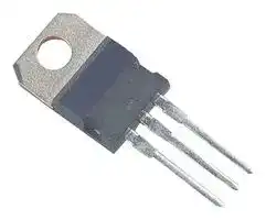
Power MOSFET, HEXFET, P Channel, 50 V, 18 A, 0.14 ohm, TO-220AB, Through Hole
- Manufacturer: VISHAY
- Product type: Single MOSFETs
- Transistor Polarity:P Channel; Continuous Drain Current Id:-18A; Drain Source Voltage Vds:-50V; On Resistance Rds(on):0.093ohm; Rds(on) Test Voltage Vgs:-10V; Threshold Voltage Vgs:-
- MSL: -
- SVHC: Lead (21-Jan-2025)
- No. of Pins: 3Pins
- Channel Type: P Channel
- Product Range: -
- Qualification: -
- Power Dissipation: 74W
- Transistor Mounting: Through Hole
- Rds(on) Test Voltage: 10V
- Transistor Case Style: TO-220AB
- Drain Source Voltage Vds: 50V
- Operating Temperature Max: 150°C
- Continuous Drain Current Id: 18A
- Drain Source On State Resistance: 0.14ohm
- Gate Source Threshold Voltage Max: 4V
| Delivery and price | |
|---|---|
| Units per pack | 5000 |
| Price | 0.73 € |
| Current stock | 500+ |
| Lead time | 30 days |
**IRF9Z30**

Vishay Siliconix

www.vishay.com

## **Power MOSFET**

**==> picture [179 x 111] intentionally omitted <==**

**----- Start of picture text -----**<br>
S<br>TO-220AB<br>G<br>S<br>, D “8<br>G D<br>P-Channel MOSFET<br>**----- End of picture text -----**<br>


|**PRODUCT SUMMARY**|**PRODUCT SUMMARY**|**PRODUCT SUMMARY**|
|---|---|---|
|VDS(V)|-50||
|RDS(on)(Ω)|VGS= -10 V|0.14|
|Qgmax. (nC)|39||
|Qgs(nC)|10||
|Qgd(nC)|15||
|Configuration|Single||


## **FEATURES**

• P-channel versatility • Compact plastic package Available • Fast switching Available • Low drive current • Ease of paralleling • Excellent temperature stability • Material categorization: for definitions of compliance RoHS

- Material categorization: for definitions of compliance please see www.vishay.com/doc?99912

- **Note**

- This    datasheet    provides    information    about    parts    that    are RoHS-compliant and / or parts that are non RoHS-compliant.  For example, parts with lead (Pb) terminations are not RoHS-compliant. Please see the information / tables in this datasheet for details

## **DESCRIPTION**

The power MOSFET technology is the key to Vishay’s advanced line of power MOSFET transistors. The efficient geometry and unique processing of the power MOSFET design achieve very low on-state resistance combined with high transconductance and extreme device ruggedness.

The p-channel power MOSFET’s are designed for application which require the convenience of reverse polarity operation. They retain all of the features of the more common n-channel Power MOSFET’s such as voltage control, very fast switching, ease of paralleling, and excellent temperature stability.

P-channel power MOSFETs are intended for use in power stages where complementary symmetry with n-channel devices offers circuit simplification. They are also very useful in drive stages because of the circuit versatility offered by the reverse polarity connection. Applications include motor control, audio amplifiers, switched mode converters, control circuits and pulse amplifiers.

|**ORDERING INFORMATION**||
|---|---|
|Package|TO-220AB|
|Lead (Pb)-free|IRF9Z30PbF|
|Lead (Pb)-free and halogen-free|IRF9Z30PbF-BE3|


|**ABSOLUTE MAXIMUM RATINGS**(TC= 25 °C, unless otherwise noted)<br>~~Cn~~|**ABSOLUTE MAXIMUM RATINGS**(TC= 25 °C, unless otherwise noted)<br>~~Cn~~|**ABSOLUTE MAXIMUM RATINGS**(TC= 25 °C, unless otherwise noted)<br>~~Cn~~|**ABSOLUTE MAXIMUM RATINGS**(TC= 25 °C, unless otherwise noted)<br>~~Cn~~|**ABSOLUTE MAXIMUM RATINGS**(TC= 25 °C, unless otherwise noted)<br>~~Cn~~|**ABSOLUTE MAXIMUM RATINGS**(TC= 25 °C, unless otherwise noted)<br>~~Cn~~|
|---|---|---|---|---|---|
|**PARAMETER**<br>~~Cn~~<br>~~a~~|||**SYMBOL**<br>~~a~~|**LIMIT**<br>~~a~~|**UNIT**<br>~~a~~|
|Drain-source voltage<br>~~oe~~|||VDS<br>~~oe~~|-50<br>~~oe~~|V<br>~~oe~~<br>~~ee~~|
|Gate-source voltage<br>~~oe~~<br>~~|~~<br>~~ee~~<br>~~ee~~|||VGS<br>~~oe~~<br>~~P~~<br>~~ee~~|± 20<br>~~oe~~<br>~~P~~<br>~~ee~~||
|Continuous drain current<br>~~re~~|VGSat -10 V<br>~~|~~<br>~~re~~<br>~~ee~~|TC= 25 °C<br>~~|~~<br>~~re~~<br>~~ee~~|ID<br>~~P~~<br>~~re~~<br>~~ee~~|-18<br>~~P~~<br>~~re~~<br>~~ee~~|A<br>~~re~~<br>~~ee~~<br>~~a~~|
|||TC= 100 °C<br>~~|~~<br>~~re~~<br>~~ee~~||-11<br>~~P~~<br>~~re~~<br>~~ee~~||
|Pulsed drain currenta<br>~~re~~<br>~~ee~~<br>~~ee~~<br>~~a~~|||IDM<br>~~re~~<br>~~ee~~<br>~~a~~|-60<br>~~re~~<br>~~ee~~<br>~~a~~||
|Linear deratingfactor<br>~~re~~<br>~~ee~~<br>~~ee~~<br>~~a~~<br>~~a~~|||~~re~~<br>~~ee~~<br>~~a~~<br>~~a~~|0.59<br>~~re~~<br>~~ee~~<br>~~a~~<br>~~a~~|W/°C<br>~~re~~<br>~~ee~~<br>~~a~~<br>~~a~~|
|Inductive current, clamped<br>~~a~~<br>~~a~~|L = 100 μH<br>~~a~~<br>~~a~~||ILM<br>~~a~~<br>~~a~~|-60<br>~~a~~<br>~~a~~|A<br>~~a~~<br>~~a~~|
|Unclamped inductive current (avalanche current)<br>~~a~~<br>~~a~~|||IL<br>~~a~~<br>~~a~~|-3.1<br>~~a~~<br>~~a~~|A<br>~~a~~<br>~~a~~|
|Maximum power dissipation<br>~~a~~<br>~~Se~~|TC= 25 °C<br>~~a~~||PD<br>~~a~~|74<br>~~a~~|W<br>~~a~~|
|Operating junction and storage temperature range<br>~~Se~~|||TJ, Tstg|-55 to +150|°C|
|Solderingrecommendations (peak temperature)c<br>~~Se~~|For 10 s|||300||


S21-1262-Rev. B, 27-Dec-2021

**1** For technical questions, contact: hvm@vishay.com

Document Number: 91459

THIS DOCUMENT IS SUBJECT TO CHANGE WITHOUT NOTICE. THE PRODUCTS DESCRIBED HEREIN AND THIS DOCUMENT ARE SUBJECT TO SPECIFIC DISCLAIMERS, SET FORTH AT www.vishay.com/doc?91000

**IRF9Z30**

www.vishay.com

Vishay Siliconix

## **THERMAL RESISTANCE RATINGS**

|**THERMAL RESISTANCE RATINGS**|**THERMAL RESISTANCE RATINGS**|**THERMAL RESISTANCE RATINGS**|**THERMAL RESISTANCE RATINGS**|**THERMAL RESISTANCE RATINGS**|
|---|---|---|---|---|
|**PARAMETER**|**SYMBOL**|**TYP.**|**MAX.**|**UNIT**|
|Maximum junction-to-ambient|RthJA|-|80|°C/W|
|Maximum junction-to-case (drain)|RthJC|-|1.7||


|**SPECIFICATIONS**(TJ= 25 °C, unless otherwise noted)|**SPECIFICATIONS**(TJ= 25 °C, unless otherwise noted)|**SPECIFICATIONS**(TJ= 25 °C, unless otherwise noted)|**SPECIFICATIONS**(TJ= 25 °C, unless otherwise noted)|||||
|---|---|---|---|---|---|---|---|
|**PARAMETER**|**SYMBOL**|**TEST CONDITIONS**||**MIN.**|**TYP.**|**MAX.**|**UNIT**|
|**Static**||||||||
|Drain-source breakdown voltage|VDS|VGS= 0 V, ID= -250 μA||-50|-|-|V|
|Gate-source threshold voltage|VGS(th)|VDS= VGS, ID= -250 μA||-2.0|-|-4.0|V|
|Gate-source leakage|IGSS|VGS= ± 20 V||-|-|± 500|nA|
|Zero gate voltage drain current|IDSS|VDS= max. rating, VGS= 0 V||-|-|-250|μA|
|||VDS= max. rating x 0.8, VGS= 0 V,<br>TJ=125 °C||-|-|-1000||
|Drain-source on-state resistance|RDS(on)|VGS= -10 V|ID= -9.3 Ab|-|0.093|0.14|Ω|
|Forward transconductance|gfs|VDS= 2 x VGS, IDS= -9 Ab||3.1|4.7|-|S|
|**Dynamic**||||||||
|Input capacitance|Ciss|VGS= 0 V,<br>VDS= -25 V,<br>f = 1.0 MHz, see fig. 9||-|900|-|pF|
|Output capacitance|Coss|||-|570|-||
|Reverse transfer capacitance|Crss|||-|140|-||
|Totalgate charge|Qg|VGS= -10 V|ID= -18 A, VDS= -0.8<br>max. rating. see fig. 17|-|26|39|nC|
|Gate-source charge|Qgs|||-|6.9|10||
|Gate-drain charge|Qgd|||-|9.7|15||
|Turn-on delay time|td(on)|VDD= -25 V, ID= -18 A,<br>Rg= 13Ω, RD= 1.3Ω, see fig. 16<br>(MOSFET switching times are<br>essentially independent of operating<br>temperature)||-|12|18|ns|
|Rise time|tr|||-|110|170||
|Turn-off delay time|td(off)|||-|21|32||
|Fall time|tf|||-|64|96||
|Gate input resistance|Rg|f = 1 MHz, open drain||0.7|-|3.9|Ω|
|**Drain-Source Body Diode Characteristics**||||||||
|Continuous source-drain diode current|IS|MOSFET symbol<br>showing the<br>integral reverse<br>p - n junction diode<br>S<br>D<br>G||-|-|-18|A|
|Pulsed diode forward currenta|ISM|||-|-|-60||
|Body diode voltage|VSD|TJ= 25 °C, IS= -18 A, VGS= 0 Vb||-|-|-6.3|V|
|Body diode reverse recovery time|trr|TJ= 25 °C, IF= -18 A, dI/dt = 100 A/μsb||54|120|250|ns|
|Body diode reverse recovery charge|Qrr|||0.20|0.47|1.1|μC|


## **Notes**

a. Repetitive rating; pulse width limited by maximum junction temperature (see fig. 14)

b. Pulse width ≤ 300 μs; duty cycle ≤ 2 %

S21-1262-Rev. B, 27-Dec-2021

Document Number: 91459

**2**

For technical questions, contact: hvm@vishay.com THIS DOCUMENT IS SUBJECT TO CHANGE WITHOUT NOTICE. THE PRODUCTS DESCRIBED HEREIN AND THIS DOCUMENT ARE SUBJECT TO SPECIFIC DISCLAIMERS, SET FORTH AT www.vishay.com/doc?91000

**IRF9Z30**

Vishay Siliconix

**==> picture [77 x 10] intentionally omitted <==**

**----- Start of picture text -----**<br>
www.vishay.com<br>**----- End of picture text -----**<br>


## **TYPICAL CHARACTERISTICS** (25 °C, unless otherwise noted)

**==> picture [200 x 164] intentionally omitted <==**

**----- Start of picture text -----**<br>
25<br>- 10 V<br>80 μs Pulse Test<br>20<br>- 8 V<br>15<br>- 7 V<br>10<br>VGS = - 5 V<br>5<br>- 5 V<br>- 4 V<br>0<br> 0            5             10           15          20          25<br>- VDS, Drain-to-Source Voltage (V)<br>, Drain Current (A)<br>D<br>- I<br>**----- End of picture text -----**<br>


**Fig. 1 - Typical Output Characteristics**

**==> picture [202 x 148] intentionally omitted <==**

**----- Start of picture text -----**<br>
10 [3]<br>Operation in this Area Limited<br>5<br>               by RDS(on)<br>2<br>10 [2] SiHF9Z30<br>10 μs<br>5 SiHF9Z32<br>100 μs<br>SiHF9Z30<br>2<br>10 SiHF9Z32 1 μs<br>5<br>10 μs<br>21 T TSingle PulseCJ = 150 °C  = 25 °C DC<br>1 2 5 10 2 5 10 [2]<br>, Drain Current (A)<br>D<br>- I<br>**----- End of picture text -----**<br>


**==> picture [121 x 10] intentionally omitted <==**

**----- Start of picture text -----**<br>
- VDS, Drain-to-Source Voltage (V)<br>**----- End of picture text -----**<br>


**Fig. 4 - Maximum Safe Operating Area**

**==> picture [200 x 164] intentionally omitted <==**

**----- Start of picture text -----**<br>
10 [2]<br>80 µs Pulse Test<br>5 VDS = 2 x VGS<br>2<br>10<br>5<br>2<br>1<br>5<br>2 TJ = 150  ° C T J  = 25 °C<br>0.1<br>0 2 4 6 8 10<br>- VGS, Gate-to-Source Voltage (V)<br>, Drain Current (A)<br>D<br>- I<br>**----- End of picture text -----**<br>


**Fig. 2 - Typical Transfer Characteristics**

**==> picture [187 x 163] intentionally omitted <==**

**----- Start of picture text -----**<br>
10<br>80 μs Pulse Test<br>VDS = 2 x VGS<br>8<br>6<br>TJ = 25 ° C<br>4<br>TJ = 150 °C<br>2<br>0<br>0 4 8 12 15 20<br>- ID, Drain Current (A)<br>, Transconductance (S)<br>fs<br>g<br>**----- End of picture text -----**<br>


**Fig. 5 - Typical Transconductance vs. Drain Current**

**==> picture [199 x 165] intentionally omitted <==**

**----- Start of picture text -----**<br>
25<br>80 μs Pulse Test<br>20 - 10 V<br>15<br>- 8 V<br>10 - 7 V<br>5 VGS = - 5 V<br>- 5 V<br>- 4 V<br>0<br>0 1 2 3 4 5<br>- VDS, Drain-to-Source Voltage (V)<br>, Drain Current (A)<br>D<br>- I<br>**----- End of picture text -----**<br>


**Fig. 3 - Typical Saturation Characteristics**

**==> picture [200 x 165] intentionally omitted <==**

**----- Start of picture text -----**<br>
10 [2]<br>5<br>2<br>10<br>TJ = 150 °C<br>5<br>2<br>1<br>5 TJ = 25  ° C<br>2<br>0.1<br>0 2 4 6 8 10<br>- VSD, Source-to-Drain Voltage (V)<br>, Reverse Drain Current (A)<br>SD<br>- I<br>**----- End of picture text -----**<br>


**Fig. 6 - Typical Source-Drain Diode Forward Voltage**

Document Number: 91459

S21-1262-Rev. B, 27-Dec-2021

**3** For technical questions, contact: hvm@vishay.com THIS DOCUMENT IS SUBJECT TO CHANGE WITHOUT NOTICE. THE PRODUCTS DESCRIBED HEREIN AND THIS DOCUMENT ARE SUBJECT TO SPECIFIC DISCLAIMERS, SET FORTH AT www.vishay.com/doc?91000

**IRF9Z30**

www.vishay.com

Vishay Siliconix

**==> picture [202 x 164] intentionally omitted <==**

**----- Start of picture text -----**<br>
1.25<br>ID = 1 mA<br>1.15<br>1.05<br>0.95<br>0.85<br>0.75<br>- 60 - 40 - 20 0 20 40 60 80 100 120 140 160<br>TJ, Junction Temperature (°C)<br>Voltage (Normalized)<br>, Drain-to-Source Breakdown<br>DS<br>V<br>**----- End of picture text -----**<br>


**Fig. 7 - Breakdown Voltage vs. Temperature**

**==> picture [202 x 166] intentionally omitted <==**

**----- Start of picture text -----**<br>
3.0<br>ID = - 18 A<br>V GS = - 10 V<br>2.4<br>1.8<br>1.2<br>0.6<br>0.0<br>- 60 - 40 - 20 0 20 40 60 80 100 120 140 160<br>TJ, Junction Temperature (°C)<br>(Normalized)<br>, Drain-to-Source On Resistance<br>DS(on)<br>R<br>**----- End of picture text -----**<br>


**Fig. 8 - Normalized On-Resistance vs. Temperature**

**==> picture [204 x 164] intentionally omitted <==**

**----- Start of picture text -----**<br>
2000<br>VGS = 0 V, f = 1 MHz<br>Ciss = Cgs + Cgd, Cds Shorted<br>1600 C rss  = C gd<br>Coss = Cds + Cgd<br>1200<br>Ciss<br>800 Coss<br>400<br>C rss<br>0<br>1 2 5 10 2 5 10 [2]<br>- VDS, Drain-to-Source Voltage (V)<br>Capacitance (pF)<br>**----- End of picture text -----**<br>


**Fig. 9 - Typical Capacitance vs. Drain-to-Source Voltage**

**==> picture [200 x 573] intentionally omitted <==**

**----- Start of picture text -----**<br>
20<br>ID = - 18 A<br>16<br>V DS = - 40 V<br>12<br>8<br>4<br>For test circuit<br>see figure 17<br>0<br>0 10 20 30 40 50<br>Qg, Total Gate Charge (nC)<br> Fig. 10 - Typical Gate Charge vs. Gate-to-Source Voltage<br>2.0<br>80 μs Pulse Test<br>1.6<br>1.2<br>VGS = - 10 V<br>0.8<br>0.4<br>VGS = - 20 V<br>0.0<br>0 12 24 36 48 60<br>- ID, Drain Current (A)<br> Fig. 11 - Typical On-Resistance vs. Drain Current<br>20<br>16<br>12 SiHF9Z30<br>8 SiHF9Z32<br>4<br>0<br>25 50 75 100 125 150<br>TC, Case Temperature (°C)<br>, Gate-to-Source Voltage (V)<br>GS<br>- V<br>, Drain to Source on Resistance<br>DS(on)<br>R<br>, Drain Current (A)<br>D<br>- I<br>**----- End of picture text -----**<br>


**Fig. 10 - Typical Gate Charge vs. Gate-to-Source Voltage**

**Fig. 12 - Maximum Drain Current vs. Case Temperature**

S21-1262-Rev. B, 27-Dec-2021

Document Number: 91459

**4** For technical questions, contact: hvm@vishay.com THIS DOCUMENT IS SUBJECT TO CHANGE WITHOUT NOTICE. THE PRODUCTS DESCRIBED HEREIN AND THIS DOCUMENT ARE SUBJECT TO SPECIFIC DISCLAIMERS, SET FORTH AT www.vishay.com/doc?91000

**IRF9Z30**

Vishay Siliconix

## www.vishay.com

**==> picture [442 x 73] intentionally omitted <==**

**----- Start of picture text -----**<br>
Vary tp to obtain L<br>required peak IL DUT VDSS VDD - VDD<br>VGS = - 10 V tp EC + IL<br>IL 0.05 Ω tp VDS<br>VDD = 0 5 8 VDS EC = 0 75 BVDS<br>**----- End of picture text -----**<br>


## **Fig. 13a - Unclamped Inductive Test Circuit**

**Fig. 13b - Unclamped Inductive Load Test Waveforms**

**==> picture [427 x 147] intentionally omitted <==**

**----- Start of picture text -----**<br>
10<br>1 0 = 0.5<br>0.2<br>0.1 P DM<br>0.05<br>0.1 0.02 t1<br>Single Pulse t2<br>(Thermal Response) Notes:<br>0.01 1.  Duty Factor, D = t 1 /t 2<br>2.  Peak Tj = PDM x ZthJC + TC<br>10 [-2]<br>10 [-5] 10 [-4] 10 [-3] 10 [-2] 0.1 1 10<br>)thJC<br>Thermal Response (Z<br>**----- End of picture text -----**<br>


t1, Rectangular Pulse Duration (s)

**Fig. 14 - Maximum Effective Transient Thermal Impedance, Junction-to-Case vs. Pulse Duration**

**==> picture [465 x 135] intentionally omitted <==**

**----- Start of picture text -----**<br>
Current - VDS<br>regulator (Isolated<br>supply)<br>RD 50 kΩ Same type<br>12 V 0.2 μF as D.U.T<br>battery 0.3 μF<br>- D<br>required peak IVary IP to obtainL D.U.T +PS G D.U.T<br>RG - 1.5 mA S<br>VGS = - 10 V tp + VDS<br>IG ID<br>Current  Current<br>sampling sampling<br>resistor resistor<br>**----- End of picture text -----**<br>


**Fig. 13 - Switching Time Test Circuit**

**Fig. 14 - Gate Charge Test Circuit**

_Vishay Siliconix maintains worldwide manufacturing capability. Products may be manufactured at one of several qualified locations. Reliability data for Silicon Technology and Package Reliability represent a composite of all qualified locations. For related documents such as package/tape drawings, part marking, and reliability data, see www.vishay.com/ppg?91459._

Document Number: 91459

S21-1262-Rev. B, 27-Dec-2021

**5**

For technical questions, contact: hvm@vishay.com THIS DOCUMENT IS SUBJECT TO CHANGE WITHOUT NOTICE. THE PRODUCTS DESCRIBED HEREIN AND THIS DOCUMENT ARE SUBJECT TO SPECIFIC DISCLAIMERS, SET FORTH AT www.vishay.com/doc?91000

**Legal Disclaimer Notice** Vishay

www.vishay.com

## **Disclaimer**

ALL PRODUCT, PRODUCT SPECIFICATIONS AND DATA ARE SUBJECT TO CHANGE WITHOUT NOTICE TO IMPROVE RELIABILITY, FUNCTION OR DESIGN OR OTHERWISE.

Vishay Intertechnology, Inc., its affiliates, agents, and employees, and all persons acting on its or their behalf (collectively, “Vishay”), disclaim any and all liability for any errors, inaccuracies or incompleteness contained in any datasheet or in any other disclosure relating to any product.

Vishay makes no warranty, representation or guarantee regarding the suitability of the products for any particular purpose or the continuing production of any product. To the maximum extent permitted by applicable law, Vishay disclaims (i) any and all liability arising out of the application or use of any product, (ii) any and all liability, including without limitation special, consequential or incidental damages, and (iii) any and all implied warranties, including warranties of fitness for particular purpose, non-infringement and merchantability.

Statements regarding the suitability of products for certain types of applications are based on Vishay's knowledge of typical requirements that are often placed on Vishay products in generic applications. Such statements are not binding statements about the suitability of products for a particular application. It is the customer's responsibility to validate that a particular product with the properties described in the product specification is suitable for use in a particular application. Parameters provided in datasheets and / or specifications may vary in different applications and performance may vary over time. All operating parameters, including typical parameters, must be validated for each customer application by the customer's technical experts. Product specifications do not expand or otherwise modify Vishay's terms and conditions of purchase, including but not limited to the warranty expressed therein.

Hyperlinks included in this datasheet may direct users to third-party websites. These links are provided as a convenience and for informational purposes only. Inclusion of these hyperlinks does not constitute an endorsement or an approval by Vishay of any of the products, services or opinions of the corporation, organization or individual associated with the third-party website. Vishay disclaims any and all liability and bears no responsibility for the accuracy, legality or content of the third-party website or for that of subsequent links.

Except as expressly indicated in writing, Vishay products are not designed for use in medical, life-saving, or life-sustaining applications or for any other application in which the failure of the Vishay product could result in personal injury or death. Customers using or selling Vishay products not expressly indicated for use in such applications do so at their own risk. Please contact authorized Vishay personnel to obtain written terms and conditions regarding products designed for such applications.

No license, express or implied, by estoppel or otherwise, to any intellectual property rights is granted by this document or by any conduct of Vishay. Product names and markings noted herein may be trademarks of their respective owners.

_**© 2023 VISHAY INTERTECHNOLOGY, INC. ALL RIGHTS RESERVED**_

Revision: 01-Jan-2023

Document Number: 91000

**1**
Updated at April 29, 2026
Vishay is a global leader in the manufacturing of discrete semiconductors and passive electronic components. Renowned for its exceptional quality and engineering expertise, the company produces highly reliable solutions that drive innovation across the industrial, automotive, telecommunications, and consumer electronics markets. From advanced factory automation to vehicle electrification, Vishay components provide the foundational building blocks for modern electronic design. The company's expansive portfolio is heavily focused on efficient power management, signal routing, and energy storage. Within its passive component lineup, Vishay is recognized for its extensive array of high-performance capacitors, including robust aluminium electrolytic, film, and polymer variants, alongside highly efficient power inductors. In the realm of discrete semiconductors, Vishay is a premier manufacturer of single and dual MOSFETs, as well as a vast selection of Schottky, Zener, and fast-recovery rectifier diodes designed for demanding power applications. Furthermore, Vishay delivers industry-leading circuit protection and thermal management solutions. With a broad offering of transient voltage suppressors (TVS diodes) and temperature-sensing NTC thermistors, these components are engineered to safeguard sensitive circuitry against both electrical and thermal overstress. By combining this vital mix of advanced discretes and passives, Vishay enables engineers to develop robust, space-saving, and highly resilient electronic systems.
About Novapart
Novapart is a B2B electronic component broker specialising in stock shortages and cost reduction. We source hard-to-find parts and identify compliant alternatives across a catalogue of 410,000+ components from 500+ manufacturers.
Learn more →Stock Shortage Specialist
When a component is unavailable, discontinued or has an unacceptable lead time, we tap into our network of vetted European and Asian distributors to source what you need — without compromising on quality or traceability.
Request a quote →Compliant Alternatives
We identify pin-to-pin, electrically equivalent substitutes that meet the same certifications (RoHS, AEC-Q100, REACH) as your original specification — validated against datasheets, not just part numbers. Often at a lower cost.
BOM Analysis service →