


IRF7501TRPBF
Dual MOSFET, N Channel, 20 V, 20 V, 2.4 A, 2.4 A, 0.085 ohm
- Manufacturer: INFINEON
- Product type: Dual MOSFETs
- Transistor Polarity:Dual N Channel; Continuous Drain Current Id:2.4A; Drain Source Voltage Vds:20V; On Resistance Rds(on):0.085ohm; Rds(on) Test Voltage Vgs:4.5V; Threshold Voltage
- MSL: MSL 1 - Unlimited
- SVHC: No SVHC (08-Jul-2021)
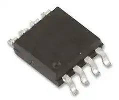
- No. of Pins: 8Pins
- Channel Type: N Channel
- Product Range: HEXFET Series
- Qualification: -
- Transistor Case Style: µSOIC
- Operating Temperature Max: 150°C
- Power Dissipation N Channel: 1.25W
- Power Dissipation P Channel: 1.25W
- Drain Source Voltage Vds N Channel: 20V
- Drain Source Voltage Vds P Channel: 20V
- Continuous Drain Current Id N Channel: 2.4A
- Continuous Drain Current Id P Channel: 2.4A
- Drain Source On State Resistance N Channel: 0.085ohm
- Drain Source On State Resistance P Channel: 0.085ohm
| Delivery and price | |
|---|---|
| Units per pack | 2000 |
| Price | 0.29 € |
| Current stock | 10+ |
| Lead time | 30 days |
PD - 95345A

## IRF7501PbF

HEXFET[®] Power MOSFET

**==> picture [413 x 101] intentionally omitted <==**

**----- Start of picture text -----**<br>
||||||||||||
|---|---|---|---|---|---|---|---|---|---|---|
|Generation V Technology|
|Ulrtra Low On-Resistance|S1|1|8|D1|
|Dual N-Channel MOSFET|G1|oo|2|LO|7|D1|VDSS =20V|
|Very Small SOIC Package|S2|3|6|D2|
|Low Profile (<1.1mm)Available in Tape & Reel|G2|“7|4|f|e|i|5|D2|RDS(on) = 0.135|Ω|
|Fast Switching|
|Top View|
|Lead-Free|

**----- End of picture text -----**<br>


## **Description**

Fifth Generation HEXFETs from International Rectifier utilize advanced processing techniques to achieve extremely low  on-resistance per silicon area.  This benefit, combined with the fast switching speed and ruggedized device design that HEXFET Power MOSFETs are well known for, provides the designer with an extremely efficient and reliable device for use in a wide variety of applications.

The new Micro8 package, with half the footprint area of the standard SO-8, provides the smallest footprint available in an SOIC outline.  This makes the Micro8 an ideal device for applications where printed circuit board space is at a premium.  The low profile (<1.1mm) of the Micro8 will allow it to fit easily into extremely thin application environments such as portable electronics and PCMCIA cards.

**==> picture [31 x 8] intentionally omitted <==**

**----- Start of picture text -----**<br>
Micro8<br>**----- End of picture text -----**<br>


## **Absolute Maximum Ratings**

**==> picture [432 x 193] intentionally omitted <==**

**----- Start of picture text -----**<br>
||||||||
|---|---|---|---|---|---|---|
|Parameter|Max.|Units|
|VDS|Drain-Source Voltage|20|V|
|ID @ TA = 25°C|Continuous Drain Current, VGS @ 10V|2.4|
|ID @ TA = 70°C|Continuous Drain Current, VGS @ 10V|1.9|A|
|ee|
|esRe|IDM|Pulsed Drain Current|©|19|_|
|eK|PD @TA = 25°C|Maximum Power Dissipation|©|(OO|1.25|W|
|IK|PD @TA = 70°C|Maximum Power Dissipation|0.8|W|
|ee(OR|Linear Derating Factor|©|(OU|0.01|W/°C|
|nD|VGSM|Gate-to-Source Voltage Single Pulse tp<10μs|16|V|
|ee|VGS|(OR|Gate-to-Source Voltage|GO|± 12|V|
|dv/dt|Peak Diode Recovery dv/dt|5.0|V/ns|
|TJ , TSTG|Operating Junction and Storage Temperature Range|-55  to + 150|°C|
|aa|Soldering Temperature, for 10 seconds|240 (1.6mm from case)|
|Thermal Resistance|
|Parameter|Max.|Units|
|R|θ|JA|Maximum Junction-to-Ambient|100|°C/W|
|eeDO|

**----- End of picture text -----**<br>


All Micro8 Data Sheets reflect improved Thermal Resistance, Power and Current -Handling Ratings- effective only for product marked with Date Code 505 or later .

www.irf.com

1

02/13/12

## **IRF7501PbF**

## **Electrical Characteristics @ TJ = 25°C (unless otherwise specified)**

|Pe|**Parameter**<br>Pe|**Min. **<br>Pe|**Typ. **<br>Pe|**Max. **<br>Pe|**Units**<br>Pe|**Conditions**<br>Pe|
|---|---|---|---|---|---|---|
|V(BR)DSS<br>~~GG~~<br>~~Re~~|Drain-to-Source Breakdown Voltage<br>~~GG~~<br>~~GC~~|20<br>~~GG~~<br>~~GC~~|–––<br>~~GG~~<br>~~GC~~|–––<br>~~GG~~<br>~~GC~~|V<br>~~GG~~<br>~~GC~~|VGS= 0V, ID= 250μA<br>~~GG~~<br>~~GC~~|
|ΔV(BR)DSS/ΔTJ <br>~~Re~~|Breakdown Voltage Temp. Coefficient<br>~~GC~~|––– <br>~~GC~~|0.041 <br>~~GC~~|–––<br>~~GC~~|V/°C<br>~~GC~~|Reference to 25°C, ID= 1mA<br>~~GC~~|
|RDS(on)<br>~~Re~~<br>~~EE~~|Static Drain-to-Source On-Resistance<br>~~GC~~<br>~~EE~~|––– <br>~~GC~~<br>~~EE~~|0.085 <br>~~GC~~<br>~~EE~~|0.135<br>~~GC~~<br>~~EE~~|Ω<br>~~GC~~<br>~~EE~~|VGS= 4.5V, ID= 1.7A<br>~~GC~~<br>~~EE~~|
|||––– <br>~~EE~~<br>~~ff~~|0.120 <br>~~EE~~<br>~~ff~~|0.20<br>~~EE~~<br>~~ff~~||VGS= 2.7V,ID= 0.85A<br>~~EE~~|
|VGS(th)<br>~~a~~|Gate Threshold Voltage<br>|0.70<br>|–––<br>|–––<br>|V<br>|VDS= VGS, ID= 250μA<br>|
|gfs<br>~~GC~~|Forward Transconductance<br>~~GC~~|2.6<br>~~GC~~|–––<br>~~GC~~|–––<br>~~GC~~|S<br>~~GC~~|VDS= 10V, ID= 0.85A<br>~~GC~~|
|IDSS<br>~~EEE~~<br>~~ee~~|Drain-to-Source Leakage Current<br>~~EEE~~|–––<br>~~EEE~~|–––<br>~~EEE~~|1.0<br>~~EEE~~|μA<br>~~EEE~~|VDS= 16V, VGS= 0V<br>~~EEE~~|
|||–––<br>~~EEE~~<br>~~ee~~|–––<br>~~EEE~~<br>~~ee~~|25<br>~~EEE~~<br>~~ee~~||VDS= 16V, VGS= 0V, TJ= 125°C<br>~~EEE~~|
|IGSS<br>~~ee~~<br>~~ee~~<br>~~a~~|Gate-to-Source Forward Leakage|–––<br>~~ee~~<br>~~3~~|–––<br>~~ee~~<br>~~3~~|100<br>~~ee~~|nA<br>I<br>~~|~~|VGS= 12V|
||Gate-to-Source Reverse Leakage<br>~~|~~<br>|–––<br>~~ee~~<br>~~3~~<br>~~|~~<br><br>~~ee~~|–––<br>~~ee~~<br>~~3~~<br>~~|~~<br><br>~~ee~~|-100<br>~~ee~~<br>~~|~~<br>||VGS= -12V<br>~~|~~|
|Qg<br>~~ee~~<br>~~ee~~<br>~~a~~|Total Gate Charge<br>~~|~~<br>~~ee~~|–––<br>~~ee~~<br>~~|~~<br>~~ee~~<br>~~ee~~|5.3<br>~~ee~~<br>~~|~~<br>~~ee~~<br>~~ee~~|8.0<br>~~ee~~<br>~~|~~<br>~~ee~~|nC<br>~~|~~|ID= 1.7A<br>VDS= 16V<br>VGS= 4.5V, See Fig. 9<br>~~|~~<br>~~C)~~|
|Qgs<br>~~ee~~<br>~~a~~<br>~~es~~|Gate-to-Source Charge<br>~~|~~<br>|–––<br>~~|~~<br><br>~~ee~~|0.84<br>~~|~~<br><br>~~ee~~|1.3<br>~~|~~<br>|||
|Qgd<br>~~es~~<br>~~ee~~|Gate-to-Drain("Miller")Charge<br>~~ee~~|–––<br>~~ee~~|2.2<br>~~ee~~|3.3<br>~~ee~~|||
|td(on)<br>~~es~~<br>~~ee~~|Turn-On DelayTime<br>~~ee~~|–––<br>~~ee~~|5.7<br>~~ee~~|–––<br>~~ee~~|ns|VDD= 10V<br>ID= 1.7A<br>RG= 6.0Ω<br>RD= 5.7Ω<br>~~C)~~<br>C)|
|tr<br>~~ee~~<br>~~a~~<br>~~ee~~|Rise Time<br>~~ee~~<br>~~ee~~|–––<br>~~ee~~<br>~~ee~~|24<br>~~ee~~<br>~~ee~~|–––<br>~~ee~~<br>~~ee~~|||
|td(off)<br>~~ee~~|Turn-Off Delay Time<br>~~ee~~|–––<br>~~ee~~|15<br>~~ee~~|–––<br>~~ee~~|||
|tf<br>~~ee~~<br>~~a~~<br>~~ee~~|Fall Time<br>~~ee~~<br>~~ee~~|–––<br>~~ee~~<br>~~ee~~|16<br>~~ee~~<br>~~ee~~|–––<br>~~ee~~<br>~~ee~~|||
|Ciss<br>~~ee~~<br>~~ee~~|Input Capacitance<br>~~ee~~<br>~~ee~~|–––<br>~~ee~~<br>~~ee~~|260<br>~~ee~~<br>~~ee~~|–––<br>~~ee~~<br>~~ee~~|pF|VGS= 0V<br>VDS= 15V<br>ƒ = 1.0MHz, See Fig. 8|
|Coss<br>~~ee~~<br>~~ee~~<br>~~ee~~|Output Capacitance<br>~~ee~~<br>~~ee~~<br>~~ee~~|–––<br>~~ee~~<br>~~ee~~<br>~~ee~~|130<br>~~ee~~<br>~~ee~~<br>~~ee~~|–––<br>~~ee~~<br>~~ee~~<br>~~ee~~|||
|Crss<br>~~ee~~<br>~~ee~~|Reverse Transfer Capacitance<br>~~ee~~<br>~~ee~~|–––<br>~~ee~~<br>~~ee~~|61<br>~~ee~~<br>~~ee~~|–––<br>~~ee~~<br>~~ee~~|||


## **Source-Drain Ratings and Characteristics**

|~~ne~~|**Parameter**<br>~~es~~|**Min. **<br>~~ee~~|**Typ. **<br>~~ee~~|**Max. **<br>~~ee~~|**Units**<br>~~ee~~|**Conditions**<br>~~ee~~|
|---|---|---|---|---|---|---|
|IS<br>~~ne~~|Continuous Source Current<br>(Body Diode)<br>~~es~~|–––<br>~~ee~~|–––<br>~~ee~~|1.25<br>~~ee~~|A<br>~~ee~~<br>~~ss~~|MOSFET symbol<br>showing  the<br>integral reverse<br>p-njunction diode.<br>S<br>D<br>G<br>~~ee~~|
|ISM<br>~~ne~~<br>~~Sn~~|Pulsed Source Current<br>(BodyDiode)<br>~~es ~~<br>~~Sn~~|–––<br> ~~ee~~<br>~~ss~~|–––<br>~~ee~~<br>~~ss~~|19<br>~~ee~~<br>~~ss~~|||
|VSD<br>~~a~~<br>~~Sn~~|Diode Forward Voltage<br>~~es~~<br>~~Sn~~|–––<br>~~es~~<br>~~ss~~|–––<br>~~es~~<br>~~ss~~|1.2<br>~~es~~<br>~~ss~~|V<br>~~es~~<br>~~ss~~|TJ= 25°C, IS= 1.7A, VGS= 0V<br>~~es~~|
|trr<br>~~Sn~~|Reverse RecoveryTime<br>~~Sn~~|–––<br>~~ss~~|39<br>~~ss~~|59<br>~~ss~~|ns<br>~~ss~~|TJ= 25°C, IF= 1.7A<br>di/dt = 100A/μs<br>~~a®~~|
|Qrr<br>~~a~~|Reverse Recovery Charge<br>~~a~~|–––<br>~~a~~|37<br>~~a~~|56<br>~~a~~|nC<br>~~a~~||


**Notes:**

@ Repetitive rating;  pulse width limited by 6) Pulse width ≤ 300μs; duty cycle ≤ 2% max. junction temperature. ( See fig. 10 )

ISD ≤ 1.7A, di/dt ≤ 66A/μs, VDD ≤ V(BR)DSS, TJ ≤ 150°C

Surface mounted on FR-4 board, t ≤ 10sec

www.irf.com

2

**IRF7501PbF**

**==> picture [434 x 198] intentionally omitted <==**

**----- Start of picture text -----**<br>
100  TOP           7.5V ver 100  TOP           7.5V Ves pay<br>                   5.0V                    5.0V<br>                   4.0V Seat oe eemeeil                    4.0V tte<br>                   3.5V                    3.5V<br>                   3.0V ss ee                    3.0V es<br>                   2.5V                    2.5V<br>10                    2.0V op Seen 10                    2.0V ge<br> BOTTOM   1.5V  BOTTOM   1.5V<br>reeee_SS eee eeeeet!eee |ee_  a ee ee eee<br>1 eo 1 700ig e el<br>1.5V<br>es a eS<br>0.1 Pie 0.1 me<br>1.5V<br>0.01  T   = 25°CJ A 0.01  T   = 150°CJ<br>0.1 ii 1 els 10 0.1 en 1 10<br>V     , Drain-to-Source Voltage (V)DS V     , Drain-to-Source Voltage (V)DS<br>I   , Drain-to-Source Current (A)D I   , Drain-to-Source Current (A)D<br>**----- End of picture text -----**<br>


## **Fig 1.** Typical Output Characteristics

## **Fig 2.** Typical Output Characteristics

**==> picture [204 x 197] intentionally omitted <==**

**----- Start of picture text -----**<br>
100 ot<br>a ee eee<br>10 ssaP|Poteeff | fy etCL<br>a eee ee eee<br>re eea eeeeeee eeeeeee eeeee<br>FA7 T  = 150°C J > il 4ee4 ee<br>4A eee ee ee<br>T  = 25°CJ<br>1 |<br>Oe ffA oe ee| ee<br>ie oe ee ee<br>ffey A | ee| {jf fT fy<br>0.1 FLTF}  V     = 10V suecys DS p ursere w ine ie<br>1.5 2.0 2.5 3.0 3.5 4.0<br>V     , Gate-to-Source Voltage (V)GS<br>D<br>I   , Drain-to-Source Current (A)<br>**----- End of picture text -----**<br>


**==> picture [203 x 197] intentionally omitted <==**

**----- Start of picture text -----**<br>
100 === = SS SS<br>ee ee ee ee eee eee eee<br>10 eeaPittyPettOa eyft ee|yyLeee ee<br>ee ee ee ee ee<br>eeee eeee eeee eeeeeeeeeeeee eee<br>ee T  = 150J ° ee C ee. ee ee ee eee<br>a Ge ee ee<br>L AY|\|<br>1 -—IZ!ff — ft — T  = 25J —I °C ||i titty| |<br>J i+<br>| [ft [fy T ft | JT [T [ J Ty Tf<br>eyee<br>0.1 P B A W P LEseeod<br>0.4 0.6 0.8 1.0 1.2 1.4 1.6 1.8<br>V     , Source-to-Drain Voltage (V)SD<br>I     , Reverse Drain Current (A)SD<br>**----- End of picture text -----**<br>


**Fig 3.** Typical Transfer Characteristics

**Fig 4.** Typical Source-Drain Diode Forward Voltage

## www.irf.com

3

## **IRF7501PbF**

**==> picture [439 x 198] intentionally omitted <==**

**----- Start of picture text -----**<br>
2.0 PPE LEE 0.8 Po<br>Cc<br>1.5 PEEE TL EEEEEL) 2 0.6 Ep fy<br>TPP PTT Lert] og<br>SL<br>1.0 [|] [ |] et 0.4 | ft fy<br>{tte [t] AT é ft<br>eee =)<br>0.5 TPE TCR}EEE TyEEE og@(a)s  Fe 0.2 Lee| Y<br>PELE 0.0<br>0.0 EEE Wid A = © 0 beset 2 [TT 4 6 [A]<br>-60 -40 -20 0 20 40 60 80 100 120 140 160<br>T   , Junction Temperature (°C)J I   , Drain Current (A)D<br> ( Ω )<br>(Normalized)<br>DS(on)<br>R           ,  Drain-to-Source On Resistance<br>**----- End of picture text -----**<br>


**Fig 5.** Normalized On-Resistance Vs. Temperature

**==> picture [178 x 20] intentionally omitted <==**

**----- Start of picture text -----**<br>
Fig 6.    Typical On-Resistance Vs. Drain<br>Current<br>**----- End of picture text -----**<br>


**==> picture [215 x 211] intentionally omitted <==**

**----- Start of picture text -----**<br>
0.13<br>0.11 Pat |  fff<br>0.09<br>0.07 PENGEt<br>0.05<br>2 3 4 5 6 7 8 [A]<br>V       , Gate-to-Source Voltage (V)GS<br> ( Ω )<br>(Ω<br>DS(on)<br>R           ,  Drain-to-Source On Resistance<br>**----- End of picture text -----**<br>


**Fig 7.** Typical On-Resistance Vs. Gate

www.irf.com

4

## **IRF7501PbF**

**==> picture [434 x 470] intentionally omitted <==**

**----- Start of picture text -----**<br>
500 10<br>V      = 0V,         f = 1MHzGS  I    = 1.7AD<br>C      = C     + C     ,   C     SHORTED iss         gs         gd         ds  V     = 16V DS<br>C      = Crss         gd<br>400 |an C      = C     + Coss        ds         gd 8 eee[ott<br>s<br>Lc! TTT 11 1Iu Pt tT<br>300 el 6 pot EY<br>ss<br>ell Pitt<br>200 SN ll 4 PE EYUY<br>ss<br>100 aSPRae 2 Pit pot YY] Kw|| ft<br>0 ell A 0 An[|]     SEE FIGURE 9 tones nc<br>1 10 100 0 2 4 6 8 10<br>V     , Drain-to-Source Voltage (V)DS Q   , Total Gate Charge (nC)G<br>Fig 9.   Typical Gate Charge Vs.<br>Fig 8.   Typical Capacitance Vs.<br>Gate-to-Source Voltage<br>Drain-to-Source Voltage<br> 1000<br> 100 A<br>eer D = 0.500.20<br>0.10<br> 10 a nn Se<br>0.05<br>PDM<br>0.02<br>rat<br>0.01 t1<br> 1 oat 0000 SINGLE PULSE te |ie t2<br>a (THERMAL RESPONSE) 1. Duty factor D =Notes: t   / t1 2<br>aee 2. Peak T J = P DM x  Z thJA + TA<br>0.1<br>0.00001 0.0001 0.001 0.01 0.1  1  10  100<br>t  , Rectangular Pulse Duration (sec)1<br>C, Capacitance (pF)<br>GS<br>-V     , Gate-to-Source Voltage (V)<br>thJA<br>(Z        )<br>Thermal Response<br>**----- End of picture text -----**<br>


**Fig 10.** Maximum Effective Transient Thermal Impedance, Junction-to-Ambient

www.irf.com

5

## **IRF7501PbF**

**==> picture [427 x 160] intentionally omitted <==**

**----- Start of picture text -----**<br>
Current Regulator<br>oO Same Type as D.U.T. 7<br>|<br>|<br>50K Ω |<br>|<br>« I QG n d 12V .2 μ F .3 μ F ||<br>LL it +<br>QGS QGD D.U.T. -VDS<br>VG VGS<br>3mA<br>ale +t Charge —> O m IG |t ID<br>Current Sampling Resistors<br>**----- End of picture text -----**<br>


**Fig 11a.** Basic Gate Charge Waveform

**Fig 11b.** Gate Charge Test Circuit

**==> picture [16 x 12] intentionally omitted <==**

**----- Start of picture text -----**<br>
 1 s<br> 0.1 %<br>**----- End of picture text -----**<br>


**Fig 12a.** Switching Time Test Circuit

**==> picture [137 x 93] intentionally omitted <==**

**----- Start of picture text -----**<br>
VDS<br>90%<br>10%<br>VGS a— > ! ‘i/r a<br>td(on) tr td(off) tf<br>**----- End of picture text -----**<br>


**Fig 12b.** Switching Time Waveforms

www.irf.com

6

## **IRF7501PbF**

**==> picture [287 x 453] intentionally omitted <==**

**----- Start of picture text -----**<br>
+ Circuit Layout Considerations<br>   •  Low Stray Inductance<br>•   Ground Plane<br> •   Low Leakage Inductance<br>| - Current Transformer<br>+<br>- - +<br>(ty<br>•   +<br>(hae •   dv/dt controlledIsp controlled by byDuty Rg Factor "D" -<br>@ •  D.U.T. - Device Under Test<br>* Reverse Polarity for P-Channel<br>** Use P-Channel Driver for P-Channel Measurements<br>oO Driver Gate Drive<br>P.W.<br>Period D =<br>P.W. | Period _t<br>VGS=10V<br>Y<br>D.U.T. ISD Waveform<br>Reverse<br>Recovery Body Diode Forward<br>Current TS) Current —\, di/dt 4 =<br>@ D.U.T. VDS Waveform<br>Diode Recovery<br>dv/dt<br>VDD<br>ma<br>Re-Applied<br>Voltage Body Diode  S Forward Drop L<br>@ Inductor Curent<br>e s ae<br>Ripple  ≤ 5% ISD<br>**----- End of picture text -----**<br>


www.irf.com

7

## **IRF7501PbF**

## Micro8 Package Outline

Dimensions are shown in milimeters (inches)

**==> picture [334 x 195] intentionally omitted <==**

**----- Start of picture text -----**<br>
LEAD ASSIGNMENTS       INCHES        MILLIMETERS<br>D DIM   MIN       MAX       MIN      MAX<br>- B - 3 D  D  D  D D1 D1 D2 D2 A       .036       .044        0.91      1.11<br>[eoHHHH 8   7   6   5 qo000HHH——_— _ —_—. 8   7   6   5 noooHHH [|LE| A1     .004       .008        0.10      0.20B       .010       .014        0.25      0.36  -}+—+—— |a ff|ff ee ee<br>7 3 E e l 8   7   6   5 H SINGLE DUAL | C       .005       .007        0.13      0.18 | | ft<br>D       .116       .120        2.95      3.05 ee<br>- A - 0.25  (.010)       M     A    M 1  2   3   4 1  2   3  4 e        .0256 BASIC        0.65 BASIC<br>L_] — 1   2   3   4 a e1      .0128 BASIC        0.33 BASIC<br>S  S  S  G S1 G1 S2 G2 E       .116       .120         2.95      3.05<br>OWoOo H       .188       .198        4.78       5.03 a ee ee<br>oy e L        .016      .026         0.41       0.66 ee ee ee ee<br>6X ——o θ           0°          6°           0°           6°<br>e 1<br>θ RECOMMENDED FOOTPRINT<br>A  1.04   0.38<br>- C - 0.10  (.004) ae ( .041 )   8X ap ( .015 )  [8X]<br>— B     8X [aor] cake A 1 L C a ee ee<br>a rr 8X 8X a<br>0.08  (.003)         M    C   A  S    B   S   3.20   4.24   5.28<br>( .126 ) ( .167 ) ( .208 )<br>NOTES:<br>       1  DIMENSIONING AND TOLERANCING PER ANSI Y14.5M-1982. oe<br>       2  CONTROLLING DIMENSION : INCH. A L    0.65<br>       3  DIMENSIONS DO NOT INCLUDE MOLD FLASH. ( .0256 ) [6X]<br>**----- End of picture text -----**<br>


## Micro8 Part Marking Information

EXAMPLE: THIS IS AN IRF7501

LOT CODE (XX) PART NUMBER

DATE CODE (YW) - See table below Y =  YEAR W =  WEEK P =  DESIGNATES LEAD - FREE PRODUCT (OPTIONAL)

WW =  (1-26) IF PRECEDED BY LAST DIGIT OF CALENDAR YEAR WW =  (27-52) IF PRECEDED BY A LETTER

|||WORK|WORK|||
|---|---|---|---|---|---|
|YEAR|Y|WEEK||W||
|2003<br>2002<br>2001<br>2004|3<br>2<br>1<br>4|03<br>02<br>01<br>04||C<br>B<br>A<br>D||
|2005|5|||||
|2006|6|||||
|2007|7|||||
|2008|8|||||
|2009<br>2010|9<br>0|26<br>24<br>25||Z<br>X<br>Y||


|||WORK|WORK|||
|---|---|---|---|---|---|
|YEAR|Y|WEEK||W||
|2001|A|27||A||
|2002|B|28||B||
|2003|C|29||C||
|2004|D|30||D||
|2005|E|||||
|2006|F|||||
|2007|G|||||
|2008|H|||||
|2009|J|||||
|2010|K|50||X||
|||51||Y||
|||52||Z||


www.irf.com

8

**IRF7501PbF**

## Micro8 Tape & Reel Information

Dimensions are shown in millimeters (inches)

**==> picture [201 x 136] intentionally omitted <==**

**----- Start of picture text -----**<br>
TERMINAL NUMBER 1<br>Oooo ©<br>12.3 ( .484 )<br>11.7 ( .461 )<br>8.1 ( .318 )7.9 ( .312 ) tL FEED DIRECTION<br>**----- End of picture text -----**<br>


**==> picture [26 x 6] intentionally omitted <==**

**----- Start of picture text -----**<br>
NOTES:<br>**----- End of picture text -----**<br>


1.   OUTLINE CONFORMS TO EIA-481 & EIA-541.

2.   CONTROLLING DIMENSION : MILLIMETER.

**==> picture [188 x 83] intentionally omitted <==**

**----- Start of picture text -----**<br>
 330.00<br>(12.992)<br>  MAX.<br>14.40 ( .566 )<br>12.40 ( .488 )<br>**----- End of picture text -----**<br>


NOTES :

1. CONTROLLING DIMENSION : MILLIMETER.

2. OUTLINE CONFORMS TO EIA-481 & EIA-541.

Data and specifications subject to change without notice. This product has been designed and qualified for the Consumer market. Qualifications Standards can be found on IR’s Web site.

**IR WORLD HEADQUARTERS:** 101N.Sepulveda blvd, El Segundo, California 90245, USA Tel: (310) 252-7105 TAC Fax: (310) 252-7903 Visit us at www.irf.com for sales contact information **.** 02/2012

www.irf.com

9
Updated at June 9, 2026
Infineon Technologies is a globally recognized leader in semiconductor solutions, renowned for driving innovation in power management, energy efficiency, and modern mobility. With a strong legacy of engineering excellence, the company provides highly reliable components designed to meet the rigorous demands of industrial, automotive, and advanced commercial applications. The core of our Infineon portfolio is centered on their industry-leading discrete semiconductors. We offer an extensive selection of single and dual MOSFETs, alongside a robust range of single IGBTs and advanced IGBT modules. These flagship power transistors are essential for high-efficiency power conversion and motor control, providing engineers with superior thermal performance and minimized switching losses. Beyond advanced field-effect transistors, the selection includes a comprehensive array of diodes and rectifiers, heavily featuring Schottky diodes, as well as fast-recovery and RF/PIN diodes. This power foundation is further supported by bipolar transistors, intelligent power modules, and thyristor SCR modules, delivering the critical building blocks required for complex power system designs. To support broader system integration, the portfolio also encompasses specialized solutions such as solid-state relays, AC/DC LED driver ICs, and Bluetooth communications modules. From high-power industrial rectifiers to wireless connectivity adapters, Infineon equips designers with the precision components needed to build efficient, scalable, and fully connected electronic systems.
About Novapart
Novapart is a B2B electronic component broker specialising in stock shortages and cost reduction. We source hard-to-find parts and identify compliant alternatives across a catalogue of 410,000+ components from 500+ manufacturers.
Learn more →Stock Shortage Specialist
When a component is unavailable, discontinued or has an unacceptable lead time, we tap into our network of vetted European and Asian distributors to source what you need — without compromising on quality or traceability.
Request a quote →Compliant Alternatives
We identify pin-to-pin, electrically equivalent substitutes that meet the same certifications (RoHS, AEC-Q100, REACH) as your original specification — validated against datasheets, not just part numbers. Often at a lower cost.
BOM Analysis service →