


IRF7341GTRPBF
Dual MOSFET, N Channel, 55 V, 55 V, 5.1 A, 5.1 A, 0.043 ohm
- Manufacturer: INFINEON
- Product type: Dual MOSFETs
- Transistor Polarity:Dual N Channel; Continuous Drain Current Id:5.1A; Drain Source Voltage Vds:55V; On Resistance Rds(on):0.043ohm; Rds(on) Test Voltage Vgs:10V; Threshold Voltage Vg
- MSL: -
- SVHC: No SVHC (25-Jun-2025)
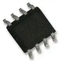
- No. of Pins: 8Pins
- Channel Type: N Channel
- Product Range: HEXFET Series
- Qualification: -
- Transistor Case Style: SOIC
- Operating Temperature Max: 175°C
- Power Dissipation N Channel: 1.7W
- Power Dissipation P Channel: 1.7W
- Drain Source Voltage Vds N Channel: 55V
- Drain Source Voltage Vds P Channel: 55V
- Continuous Drain Current Id N Channel: 5.1A
- Continuous Drain Current Id P Channel: 5.1A
- Drain Source On State Resistance N Channel: 0.043ohm
- Drain Source On State Resistance P Channel: 0.043ohm
| Delivery and price | |
|---|---|
| Units per pack | 2000 |
| Price | 0.655 € |
| Current stock | 1000+ |
| Lead time | 30 days |
- Advanced Process Technology

- Dual N-Channel MOSFET

- Ultra Low On-Resistance

- 75°C Operating Temperature

- Repetitive Avalanche Allowed up to Tjmax

||~~_IRF7341GPbF~~|~~_IRF7341GPbF~~|
|---|---|---|
||HEXFET®Power MOSFET||
|**VDSS**<br>**55V**|**RDS(on) max**<br>0.050@VGS= 10V<br>0.065@VGS= 4.5V|**ID**<br>5.1A<br>4.42A|


- ead-Free

-

## **Description**

These HEXFET ® Power MOSFET’s in a Dual SO-8 package utilize the lastest processing techniques to achieve extremely low on-resistance per silicon area. Additional features of these HEXFET Power MOSFET’s are a 175°C junction operating temperature, fast switching speed and improved repetitive avalanche rating. These benefits combine to make this design an extremely efficient and reliable device for use in a wide variety of other applications.

**==> picture [168 x 82] intentionally omitted <==**

**----- Start of picture text -----**<br>
S1 1 8 TD D1<br>G1 2 7 “TO D1<br>S2 3 6 10 D2<br>G2 4 5 TT D2<br>SO-8<br>Top View<br>**----- End of picture text -----**<br>


The 175°C rating for the SO-8 package provides improved thermal performance with increased safe operating area and dual MOSFET die capability make it ideal in a variety of power applications. This dual, surface mount SO-8 can dramatically reduce board space and is also available in Tape & Reel.

|**Base Part  Number**|**Package Type**|**Standard Pack**|**Standard Pack**|**Orderable Part Number**|
|---|---|---|---|---|
|||**Form**|**Quantity**||
|IRF7341GPbF|SO-8|Tube/Bulk|95|IRF7341GPbF|
|||Tape andReel|4000|IRF7341GTRPbF|


## **Absolute Maximum Ratings**

||**Parameter**|**Max.**|**Units**|
|---|---|---|---|
|VDS<br>~~os~~<br>~~TT~~|Drain-Source Voltage<br>~~os~~<br>~~TT~~|55<br>~~os~~<br>~~WT~~|V<br>~~os~~<br>~~WT~~|
|ID@ TA= 25°C<br>~~TT~~|Continuous Drain Current, VGS@ 10V<br>~~TT~~|5.1<br>~~WT~~|A<br>~~WT~~|
|ID@ TA= 70°C<br>~~TT~~<br>~~a~~|Continuous Drain Current, VGS@ 10V<br>~~TT~~<br>~~a~~|4.2<br>~~WT~~<br>~~a~~||
|IDM<br>~~a~~|Pulsed Drain Current<br>~~a~~|42<br>~~a~~||
|PD@TA= 25°C<br>~~a~~|Maximum Power Dissipation<br>~~a~~|2.4<br>~~a~~|W|
|PD@TA= 70°C<br>~~a~~|Maximum Power Dissipation<br>~~a~~|1.7<br>~~a~~|W|
|Linear Deratin<br>~~a~~|Linear DeratingFactor                                                                      16                               mW/°C<br>~~a~~<br>~~a~~|Factor                                                                      16                               mW/°C<br>~~a~~|Factor                                                                      16                               mW/°C|
|VGS<br>~~a~~|GSGate-to-Source Voltage<br>± 20|± 20|V|
|EAS<br>~~oes~~|Single Pulse Avalanche Energy<br>~~oes~~|140<br>~~oes~~|mJ<br>~~oes~~|
|IAR<br>~~©~~|Avalanche Current<br>~~©~~|5.1<br>~~©~~|A<br>~~©~~|
|EAR<br>~~a~~|Repetitive Avalanche Energy<br>~~a~~|See Fig. 14, 15, 16<br>~~a~~|mJ<br>~~a~~<br>~~ZO~~|
|TJ, TSTG<br>~~oo~~|Junction and Storage Temperature Range<br>~~oo~~|-55  to + 175<br>~~oo~~|°C<br>~~oo~~<br>~~ZO~~|


## **Thermal Resistance**

## **Electrical Characteristics @ TJ = 25°C (unless otherwise specified)**

|~~po~~|**Parameter**<br>ef<br>~~po~~|**Min. **<br>ef|**Typ. **<br>ef<br>~~fe~~|**Max.**<br>ef<br>~~Os~~|**Units**<br>ef<br>~~Os~~|**Conditions**<br>ef|
|---|---|---|---|---|---|---|
|V(BR)DSS<br>~~po~~|Drain-to-Source Breakdown Voltage<br>~~sO~~<br>~~po~~|55<br>~~sO~~|–––<br>~~sO~~<br>~~fe~~|–––<br>~~Os~~<br>~~sO~~|V<br>~~Os~~<br>~~sO~~|VGS= 0V, ID= 250μA<br>~~sO~~|
|ΔV(BR)DSS/ΔTJ<br>~~po~~|Breakdown Voltage Temp. Coefficient<br>~~po~~|––– <br>~~[|~~|0.052<br>~~fe~~<br>~~[|~~|–––<br>|V/°C<br>~~ee~~|Reference to 25°C, ID= 1mA<br>~~ee~~|
|RDS(on)<br>~~po~~|Static Drain-to-Source On-Resistance<br>~~po~~<br>~~ee~~|––– <br>~~ee~~<br>~~[|~~|0.043 <br>~~fe~~<br>~~ee~~<br>~~[|~~|0.050<br>~~ee~~<br>|Ω<br>~~ee~~<br>~~ee~~|VGS= 10V, ID= 5.1A<br>~~ee~~<br>~~ee~~|
|||~~ee~~<br>~~[|~~|0.056 <br>~~ee~~<br>~~[||~~|0.065<br>~~ee~~<br>~~|~~||VGS= 4.5V,ID= 4.42A<br>~~ee~~<br>~~ee~~|
|VGS(th)|Gate Threshold Voltage<br>~~Oe~~|1.0<br>~~[|~~<br>~~Oe~~|–––<br>~~[| ~~<br>~~Oe~~|–––<br><br>|V<br>~~ee~~<br>~~GC~~|VDS= VGS, ID= 250μA<br>~~ee~~<br>~~GC~~|
|gfs|Forward Transconductance<br>~~fs~~|10.4<br>~~fs~~|–––<br>~~fs~~|–––<br>~~fs~~|S<br>~~fs~~|VDS= 10V, ID= 5.2A<br>~~fs~~|
|IDSS|Drain-to-Source Leakage Current<br>~~ee~~|–––<br>~~ee~~|–––<br>~~ee~~|2.0<br>~~ee~~|~~ee~~<br>~~ee~~|VDS= 44V,VGS= 0V<br>~~ee~~|
|||–––<br>~~ee~~<br>~~ee~~|–––<br>~~ee~~<br>~~ee~~|25<br>~~ee~~<br>~~ee~~||VDS= 44V, VGS= 0V, TJ= 150°C<br>~~ee~~<br>~~ee~~|
||Gate-to-Source Forward Leakage<br>~~8~~<br>~~ee~~|–––<br>~~8~~|–––<br>~~8~~|100<br>~~8~~|~~8~~<br>~~po~~|VGS= 20V<br>~~8~~<br>~~po~~|
||Gate-to-Source Reverse Leakage<br>~~8~~<br>~~ee~~|–––<br>~~8~~<br>~~oe~~|–––<br>~~8~~<br>~~oe~~|-100<br>~~8~~||VGS= -20V<br>~~8~~<br>~~po~~|
|Qg|Total Gate Charge<br>~~ee~~<br>~~**e**e~~|–––<br>~~e~~<br>~~oe~~|29<br>~~e~~<br>~~oe~~|44<br>~~e~~|nC<br>~~po~~|ID= 5.2A<br>VDS= 44V<br>VGS= 10V<br>~~po~~|
|Qgs|Gate-to-Source Charge<br>~~**e**e~~<br>~~e~~|–––<br>~~e~~<br>~~oe~~<br>~~e~~|2.9<br>~~e~~<br>~~oe~~<br>~~e~~|4.4<br>~~e~~|||
|Qgd|Gate-to-Drain("Miller")Charge<br>~~po~~|–––<br>~~oe ~~<br>~~po~~|7.3<br> ~~oe~~<br>~~po~~|11<br>~~po~~|||
|td(on)|Turn-On DelayTime<br>~~ee~~|–––<br>~~ee~~<br>~~ee~~|9.2<br>~~ee~~<br>~~ee~~|–––<br>~~ee~~||VDD= 28V<br>ID= 1.0A<br>RG= 6.0Ω<br>VGS= 10V<br>~~@~~|
|tr|Rise Time<br>~~ee~~<br>~~ee~~|–––<br>~~ee~~<br>~~ee~~<br>~~ee~~|7.7<br>~~ee~~<br>~~ee~~<br>~~ee~~|–––<br>~~ee~~|||
|td(off)|Turn-Off Delay Time<br>~~ee~~<br>~~ee~~<br>~~ee~~|–––<br>~~ee~~<br>~~ee~~<br>~~ee~~|31<br>~~ee~~<br>~~ee~~<br>~~ee~~|–––<br>~~ee~~|||
|tf|Fall Time<br>~~ee~~<br>~~ee~~|–––<br>~~ee~~|12.5<br>~~ee~~|–––|||
|Ciss|Input Capacitance<br>~~ee~~<br>~~ee~~|–––<br>~~ee~~|780<br>~~ee~~|–––|pF|VGS= 0V<br>VDS= 25V<br>ƒ = 1.0MHz<br>~~@~~|
|Coss|Output Capacitance<br>~~ee~~<br>~~ee~~|–––<br>~~ee~~<br>~~ee~~|190<br>~~ee~~<br>~~ee~~|–––|||
|Crss|Reverse Transfer Capacitance<br>~~ee~~|–––<br>~~ee~~|66<br>~~ee~~|–––|||


## **Source-Drain Ratings and Characteristics**

a IS Continuous Source Current **Parameter Min.** ~~GO~~ **Typ. Max. Units** MOSFET symbol **Conditions** D 2.4 (Body Diode) showing  the ISM Pulsed Source Current integral reverse G 42 ~~EO~~ (Body Diode) p-n junction diode. S ~~po~~ VSD Diode Forward Voltage ––– ––– 1.2 V TJ = 25°C, IS = 2.6A, VGS = 0V trr Reverse Recovery Time ––– 51 77 ns TJ = 25°C, IF = 2.6A ~~eees~~ Qrr Reverse Recovery Charge ––– 76 114 ~~es~~ nC di/dt = 100A/μs @

® Repetitive rating;  pulse width limited by max. junction temperature. 0) Pulse width ≤ 300μs : duty cycle ≤ 2%.

Surface mounted on  FR-4 board, t ≤ 10sec

**==> picture [436 x 473] intentionally omitted <==**

**----- Start of picture text -----**<br>
100 100<br>VGS VGS<br>TOP          15.0V TOP          15.0V<br>                 10.0V                  10.0V<br>                  7.0V                   7.0V<br>                  5.5V                   5.5V<br>an) Zeenun                   4.5V PUTT gt                   4.5V<br>                  4.0V                   4.0V<br>10                   3.5V 10                   3.5V<br>BOTTOM    2.7V BOTTOM    2.7V<br>2.7V<br>2.7V<br>"dvAil il >AA<br>1 1<br>A ELIE | ” MOAN<br>20μs PULSE WIDTH 20μs PULSE WIDTH<br>Tj = 25°C Tj = 175°C<br>0.1 SPL LIER HEHil 0.1 Swlll |eHE<br>0.1 1 10 100 0.1 1 10 100<br>VDS, Drain-to-Source Voltage (V) VDS, Drain-to-Source Voltage (V)<br>Fig 1.   Typical Output Characteristics Fig 2.   Typical Output Characteristics<br> 100 2.5<br>eeeeeeeeeeee ID = 5.2A<br>T  = 25  CJJ ° 2.0<br>> aoe<br>4 PELLET EET et<br>A T  = 175  CJJ ° 1.5 PLE er<br> 10 A)<br>a a se es ee ee eee<br>1.0<br>a<br>ay As OO || Lert<br>A ee >TATOO<br>PALLET EEL<br>0.5<br>44-4 |<br>PEALE LEAL<br>V      = 25VDSDS<br> 1 Petit 20μs PULSE WIDTH 0.0 CECEEEE VGS EEL = 10V<br>2.0 3.0 4.0 5.0 6.0 7.0 -60 -40 -20 0 20 40 60 80 100 120 140 160 180<br>V     , Gate-to-Source Voltage (V)GS T  , Junction TemperatureJ (  C)°<br>(Normalized)<br>D<br>I   ,  Drain-to-Source Current (A)<br>DS(on)<br>R            , Drain-to-Source On Resistance<br>ID, Drain-to-Source Current (A) ID, Drain-to-Source Current (A)<br>**----- End of picture text -----**<br>


**==> picture [198 x 192] intentionally omitted <==**

**----- Start of picture text -----**<br>
 100 eeeeeeeeeeee<br>T  = 25  CJJ °<br>> aoe<br>4<br>A T  = 175  CJJ °<br> 10 A)<br>a a se es ee ee eee<br>a<br>ay As OO<br>A ee<br>44-4<br>V      = 25VDSDS<br>Petit 20μs PULSE WIDTH<br> 1<br>2.0 3.0 4.0 5.0 6.0 7.0<br>V     , Gate-to-Source Voltage (V)GS<br>D<br>I   ,  Drain-to-Source Current (A)<br>**----- End of picture text -----**<br>


**Fig 3.** Typical Transfer Characteristics

**Fig 4.** Normalized On-Resistance Vs. Temperature

**==> picture [439 x 473] intentionally omitted <==**

**----- Start of picture text -----**<br>
1400 VGS   = 0V,       f = 1 MHZ 20 ID = 5.2A VDS = 44V<br>C iss  = Cgs  + Cgd ,   Cds  VDS = 27V<br>1200 p+ SHORTED eee VDS = 11V<br>+ C   = C 16 | | | NE<br>rss   gd<br>1000 ==: Coss   = Cds + Cgd COE<br>800 — eae Ciss 12 PTT TY<br>600<br>8<br>400<br>Coss 4<br>200<br>petFPR Crss Attt it<br>0 0 VY} {| | ft ft f t t<br>1 10 100 0 10 20 30 40 50<br>VDS, Drain-to-Source Voltage (V) Q   , Total Gate Charge (nC)G<br>Fig 5.   Typical Capacitance Vs. Fig 6.   Typical Gate Charge Vs.<br>Drain-to-Source Voltage Gate-to-Source Voltage<br> 100  1000<br>OPERATION IN THIS AREA LIMITED<br>BY R<br>DS(on)<br>T  = 175  C J ° a=)<br> 100<br> 10 COT Se<br>po ff T  = 25  CJ °  10 PETCASI SSES 10us 100us rH<br>1ms<br> 1<br> 1 10ms<br> T TCJ == 175  C 25  C° °<br>SHAR V      = 0 V GS OLS  Single Pulse<br>0.1 0.1<br>0.2 0.5 0.8 1.1 1.4 0.1  1  10  100  1000<br>V     ,Source-to-Drain Voltage (V)SD V     , Drain-to-Source Voltage (V)DS<br>GS<br>V     , Gate-to-Source Voltage (V)<br>I   , Drain Current (A) D<br>I     , Reverse Drain Current (A)SD<br>C, Capacitance(pF)<br>**----- End of picture text -----**<br>


**Fig 7.** Typical Source-Drain Diode Forward Voltage

**Fig 8.** Maximum Safe Operating Area

**==> picture [406 x 238] intentionally omitted <==**

**----- Start of picture text -----**<br>
6.0 PT te TEE Vos ><br>5.0 Pi tT TTT tT TTT tT Vee<br>PE EE | D.U.T. +<br>4.0 PT TN eT = - Von<br>3.0 pit]Pt PN TEE ≤ 1<br>≤ 0.1 %<br>Pi TE T TEETEENAA ETEEL }}Pusey10V bs<br>2.0 Pte EET EP EN :<br>ER ReeeNe Fig 10a.   Switching Time Test Circuit<br>1.0 Pt TT ET EE TE TEN<br>VDS<br>Pt} Tt tT TT tT ty 90% [TN<br>0.0<br>25 50 75 100 125 150 175<br>T   , Case TemperatureC (  C)°<br>Pitt tT Eee ty ty 10% / \ OVA<br>Fig 9.   Maximum Drain Current Vs. VGS LY<br>td(on) tr td(off) tf<br>I   , Drain Current (A)D<br>**----- End of picture text -----**<br>


**Fig 9.** Maximum Drain Current Vs. Case Temperature

**Fig 10b.** Switching Time Waveforms

**==> picture [420 x 191] intentionally omitted <==**

**----- Start of picture text -----**<br>
 100<br>es D = 0.50<br>0.20<br> 10<br>0.10<br>0.05<br>Rr 0.02 HEE<br> 1<br>Scan 0.01 ca<br>P DM<br>|_| | ee SINGLE PULSE a t1<br>0.1 at (THERMAL RESPONSE) t 2<br>Notes:<br>ny en ee ee ee 1. Duty factor D = t   / t1 2<br>a ee 2. Peak T J = P DM x  Z thJA + TA<br>0.01<br>0.00001 0.0001 0.001 0.01 0.1  1  10  100<br>t  , Rectangular Pulse Duration (sec)1<br>thJA<br>(Z        )<br>Thermal Response<br>**----- End of picture text -----**<br>


**Fig 10.** Maximum Effective Transient Thermal Impedance, Junction-to-Ambient

**==> picture [435 x 518] intentionally omitted <==**

**----- Start of picture text -----**<br>
0.070 0.100<br>0.060<br>0.080<br>0.050 Py| i | | | eePeery ee<br>0.060<br>0.040<br>VGS = 4.5V<br>PRT ID = 7.1A 0.040 A<br>0.030<br>VGS = 10V<br>0.020 PERKSKE] 0.020 esEEE<br>2.0 4.0 6.0 8.0 10.0 12.0 14.0 16.0 0 10 20 30 40 50 60<br>VGS, Gate -to -Source Voltage  (V) ID , Drain Current ( A )<br>Fig 11.    Typical On-Resistance Vs. Fig 12.    Typical On-Resistance Vs.<br>Gate Voltage Drain Current<br>QGG<br>40 [[c]] [[St]] 400<br>QGSGS QGDGD I D<br>\ TOITI TOP 2.1A<br>4.3A<br>GHaanane<br>VGG 320 Ne BOTTOM 5.1A<br>Charge = 240 PAPE Er<br>Fig 13a.   Basic Gate Charge Waveform CORDEO<br>OO Current Regulator 160 PANE<br>Same Type as D.U.T.<br>50K Ω<br>12V .2 μ F 80<br>p l at .3 μ F : KTNOLL<br>UTES + PSSA EEE<br>D.U.T. -VDSVDSDS<br>0<br>VGSGS 25 50 75 100 125 150 175<br>°<br>3mA a PP Starting Tj, Junction Temperature SSISNE (   C)<br>O nl. IGG IDD | PSS<br>Current Sampling Resistors Fig 14.   Maximum Avalanche Energy<br>Vs. Drain Current<br>AS<br>E     , Single Pulse Avalanche Energy (mJ)<br> )<br>) Ω RDS ( on ) , Drain-to-Source On Resistance (<br>Ω RDS(on),  Drain-to -Source On Resistance (<br>**----- End of picture text -----**<br>


**==> picture [175 x 264] intentionally omitted <==**

**----- Start of picture text -----**<br>
QGG<br>40 [[c]] [[St]]<br>QGSGS QGDGD<br>\<br>VGG<br>Charge =<br>Fig 13a.   Basic Gate Charge Waveform<br>OO Current Regulator<br>Same Type as D.U.T.<br>50K Ω<br>12V .2 μ F<br>p l at .3 μ F :<br>UTES +<br>D.U.T. -VDSVDSDS<br>VGSGS<br>a<br>3mA<br>O nl. IGG IDD |<br>Current Sampling Resistors<br>Fig 13b.   Gate Charge Test Circuit<br>**----- End of picture text -----**<br>


## �����������

**==> picture [443 x 477] intentionally omitted <==**

**----- Start of picture text -----**<br>
100<br>Duty Cycle = Single Pulse<br>10<br>Allowed avalanche Current vs<br>avalanche  pulsewidth,  tav<br>1 0.01 assuming  Δ Tj = 25°C due to<br>avalanche losses<br>0.05<br>0.1 0.10<br>0.01<br>0.001<br>1.0E-06 1.0E-05 1.0E-04 1.0E-03 1.0E-02 1.0E-01 1.0E+00 1.0E+01 1.0E+02<br>tav (sec)<br>Fig 15.   Typical Avalanche Current Vs.Pulsewidth<br>140 Notes on Repetitive Avalanche Curves , Figures 15, 16:<br>TOP          Single Pulse                 (For further info, see AN-1005 at www.irf.com)<br>120 BOTTOM   10% Duty Cycle 1. Avalanche failures assumption:<br>ID = 5.1A  Purely a thermal phenomenon and failure occurs at a<br>    temperature far in excess of Tjmax. This is validated for<br>100     every part type.<br>2. Safe operation in Avalanche is allowed as long asTjmax is<br>80   not exceeded.<br>3. Equation below based on circuit and waveforms shown in<br>  Figures 12a, 12b.<br>60 4. PD (ave) = Average power dissipation per single<br>    avalanche pulse.<br>40 5. BV = Rated breakdown voltage (1.3 factor accounts for<br>    voltage increase during avalanche).<br>20 6. Iav = Allowable avalanche current.<br>7.  Δ T = Allowable rise in junction temperature, not to exceed<br>    Tjmax (assumed as 25°C in Figure 15, 16).<br>0   tav = Average time in avalanche.<br>25 50 75 100 125 150 175   D = Duty cycle in avalanche =  tav ·f<br>Starting TJ , Junction Temperature (°C)   ZthJC(D, tav) = Transient thermal resistance, see figure 11)<br>EAR , Avalanche Energy (mJ)<br>Avalanche Current (A)<br>**----- End of picture text -----**<br>


**Fig 16.** Maximum Avalanche Energy Vs. Temperature

**==> picture [133 x 31] intentionally omitted <==**

**----- Start of picture text -----**<br>
PD (ave) = 1/2 ( 1.3·BV·Iav) = � T/ ZthJC<br>Iav = 2 � T/ [1.3·BV·Zth]<br>EAS (AR) = PD (ave)·tav<br>**----- End of picture text -----**<br>


� ����������� ����������������������������������������������������������� �����������������������

## **SO-8 Package Outline** (Mosfet & Fetky)

Dimensions are shown in milimeters (inches)

**==> picture [363 x 315] intentionally omitted <==**

**----- Start of picture text -----**<br>
INCHES MILLIMETERS<br>DIM<br>D B MIN MAX MIN MAX<br>A 5 A .0532 .0688 1.35 1.75<br>| || | {| | |<br>— ti q 8 oot 7 ) a ot 6 a tdg 5 ||Ee A1bc || .0040.013.0075 || SE .0098.0098.020 {|{| 0.190.100.33 |]| 0.250.250.51 ||<br>6 H | D | .189 | .1968 {| 4.80 | 5.00 |<br>E 0.25 [.010]  A | E | .1497 | .1574 | 3.80 | 4.00 |<br>1 2 3 4<br>e .050  BASIC 1.27  BASIC<br>— E—ow eees e1 .025  BASIC ee 0.635  BASIC ee<br>c o p a 8 | | | [| H | .2284 [| [ff] .2440 5.80 6.20<br>K .0099 .0196 0.25 0.50<br>6X cH e ! w R | | L | | .016 | | ffff .050 0.40 1.27 |<br>y  0°  8°  0°  8°<br>| [| [| Jf J |<br>e1 K x 45°<br>A<br>_———FL]| C y + a<br>0.10 [.004]<br>( CAHEEL e 8X b A1 | [ : eLe 8X L o 8X c 4<br>le 0.25 [.010]  @] C | A B 7<br>FOOTPRINT<br>1.  DIMENSIONING & TOLERANCING PER ASME Y14.5M-1994. 8X 0.72 [.028]<br>3.  DIMENSIONS ARE SHOWN IN MILLIMETERS [INCHES].<br>4.  OUTLINE CONFORMS TO JEDEC OUTLINE MS-012AA.<br>5   DIMENSION DOES NOT INCLUDE MOLD PROTRUSIONS.     MOLD PROTRUSIONS NOT TO EXCEED 0.15 [.006].     MOLD PROTRUSIONS NOT TO EXCEED 0.15 [.006]. rT T<br>6   DIMENSION DOES NOT INCLUDE MOLD PROTRUSIONS. 6.46 [.255] bol ot<br>     MOLD PROTRUSIONS NOT TO EXCEED 0.25 [.010].<br>7   DIMENSION IS THE LENGTH OF LEAD FOR SOLDERING TO og | | | |<br>3X 1.27 [.050] a a o k<br>8X 1.78 [.070]<br>**----- End of picture text -----**<br>


NOTES:

1.  DIMENSIONING & TOLERANCING PER ASME Y14.5M-1994.

2.  CONTROLLING DIMENSION: MILLIMETER

3.  DIMENSIONS ARE SHOWN IN MILLIMETERS [INCHES]. 4.  OUTLINE CONFORMS TO JEDEC OUTLINE MS-012AA.

- ~~O~~ 5   DIMENSION DOES NOT INCLUDE MOLD PROTRUSIONS.     MOLD PROTRUSIONS NOT TO EXCEED 0.15 [.006].     MOLD PROTRUSIONS NOT TO EXCEED 0.15 [.006]. ~~O~~ 6   DIMENSION DOES NOT INCLUDE MOLD PROTRUSIONS. MOLD PROTRUSIONS NOT TO EXCEED 0.25 [.010].

- ~~:~~ 7   DIMENSION IS THE LENGTH OF LEAD FOR SOLDERING TO A SUBSTRATE.

## SO-8 Part Marking Information

EXAMPLE: THIS IS AN IRF8707GPBF

- DATE CODE (YWW) P =  DISGNATES LEAD - FREE PRODUCT

- Y =  LAST DIGIT OF THE YEAR

- ~~~~~ XXXX WW =  WEEK

- INTERNATIONAL aT ~~so~~ F8707G ft A =  ASSEMBLY SITE CODE RECTIFIER LOT CODE LOGO ~~() S~~ N PART NUMBER (G DESIGNATES HALOGEN-FREE

## **SO-8 Tape and Reel**

Dimensions are shown in millimeters (inches)

**==> picture [208 x 254] intentionally omitted <==**

**----- Start of picture text -----**<br>
TERMINAL NUMBER 1<br>oOo Oo<br>12.3 ( .484 )<br>11.7 ( .461 )<br>8.1 ( .318 )7.9 ( .312 ) | FEED DIRECTION<br>NOTES:<br>1.   CONTROLLING DIMENSION : MILLIMETER.<br>2.   ALL DIMENSIONS ARE SHOWN IN MILLIMETERS(INCHES).<br>3.   OUTLINE CONFORMS TO EIA-481 & EIA-541.<br>|  330.00<br>(12.992)<br>  MAX.<br>14.40 ( .566 )<br>12.40 ( .488 )<br>**----- End of picture text -----**<br>


NOTES :

**==> picture [100 x 4] intentionally omitted <==**

**----- Start of picture text -----**<br>
1. CONTROLLING DIMENSION : MILLIMETER.<br>**----- End of picture text -----**<br>


2. OUTLINE CONFORMS TO EIA-481 & EIA-541.

## **Qualification information** †

|**Qualification information**<br>†|||
|---|---|---|
|Qualification level|Industrial<br>(per JEDEC JESD47F<br>††guidelines)||
|Moisture Sensitivity Level|SO-8|MS L1<br>(per JEDEC J-STD-020D<br>††)|
|RoHS compliant|(per JEDEC J<br>)<br>Yes||


- Qualification standards can be found at International Rectifier’s web site: http://www.irf.com/product-info/reliability ††   Applicable version of JEDEC standard at the time of product release

**IR WORLD HEADQUARTERS:** 101 N. Sepulveda Blvd., El Segundo, California 90245, USA To contact International Rectifier, please visit http://www.irf.com/whoto-call/
Updated at June 9, 2026
Infineon Technologies is a globally recognized leader in semiconductor solutions, renowned for driving innovation in power management, energy efficiency, and modern mobility. With a strong legacy of engineering excellence, the company provides highly reliable components designed to meet the rigorous demands of industrial, automotive, and advanced commercial applications. The core of our Infineon portfolio is centered on their industry-leading discrete semiconductors. We offer an extensive selection of single and dual MOSFETs, alongside a robust range of single IGBTs and advanced IGBT modules. These flagship power transistors are essential for high-efficiency power conversion and motor control, providing engineers with superior thermal performance and minimized switching losses. Beyond advanced field-effect transistors, the selection includes a comprehensive array of diodes and rectifiers, heavily featuring Schottky diodes, as well as fast-recovery and RF/PIN diodes. This power foundation is further supported by bipolar transistors, intelligent power modules, and thyristor SCR modules, delivering the critical building blocks required for complex power system designs. To support broader system integration, the portfolio also encompasses specialized solutions such as solid-state relays, AC/DC LED driver ICs, and Bluetooth communications modules. From high-power industrial rectifiers to wireless connectivity adapters, Infineon equips designers with the precision components needed to build efficient, scalable, and fully connected electronic systems.
About Novapart
Novapart is a B2B electronic component broker specialising in stock shortages and cost reduction. We source hard-to-find parts and identify compliant alternatives across a catalogue of 410,000+ components from 500+ manufacturers.
Learn more →Stock Shortage Specialist
When a component is unavailable, discontinued or has an unacceptable lead time, we tap into our network of vetted European and Asian distributors to source what you need — without compromising on quality or traceability.
Request a quote →Compliant Alternatives
We identify pin-to-pin, electrically equivalent substitutes that meet the same certifications (RoHS, AEC-Q100, REACH) as your original specification — validated against datasheets, not just part numbers. Often at a lower cost.
BOM Analysis service →