


IRF7303TRPBFXTMA1
Dual MOSFET, Dual N Channel, 30 V, 4.9 A, 0.05 ohm
- Manufacturer: INFINEON
- Product type: Dual MOSFETs
- SVHC: No SVHC (25-Jun-2025)
- No. of Pins: 8Pins
- Channel Type: Dual N Channel
- Product Range: HEXFET Series
- Qualification: -
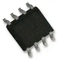
- Transistor Case Style: SO-8
- Operating Temperature Max: 150°C
- Power Dissipation N Channel: 2W
- Power Dissipation P Channel: -
- Drain Source Voltage Vds N Channel: 30V
- Drain Source Voltage Vds P Channel: -
- Continuous Drain Current Id N Channel: 4.9A
- Continuous Drain Current Id P Channel: -
- Drain Source On State Resistance N Channel: 0.05ohm
- Drain Source On State Resistance P Channel: -
| Delivery and price | |
|---|---|
| Units per pack | 5000 |
| Price | 0.232 € |
| Current stock | 1000+ |
| Lead time | 30 days |
**==> picture [96 x 84] intentionally omitted <==**

**----- Start of picture text -----**<br>
S1 1 8 D1<br>G1 _| 2 | ) a 7 Lo D1<br>S2 3 6 D2<br>G2 “T] 4 (at Pr 5 D2<br>a<br>Top View<br>**----- End of picture text -----**<br>


**==> picture [10 x 9] intentionally omitted <==**

**----- Start of picture text -----**<br>
Ω<br>**----- End of picture text -----**<br>


**==> picture [27 x 10] intentionally omitted <==**

**----- Start of picture text -----**<br>
SO-8<br>**----- End of picture text -----**<br>


**==> picture [422 x 343] intentionally omitted <==**

**----- Start of picture text -----**<br>
∆ ∆<br>Ω<br>Rpsion) Static Drain-to-Source On-Resistance |= | | 050 Ves = 10V, Ip = 2.4A ©<br>Gate |——- |— .080 Vas = 4.5V, Ip = 2.0A @<br>Threshold Voltage 11.0 |—- |—— | V_ | Vos = Ves, Ip = 250HA<br>Forward Transconductance }5.2[—-|—-[ s | Vos = 15V, Ip = 2.4A<br>loss Drain-to-Source Leakage Current |— |— |10 | HA Vos = 24V, Ves = OV<br>Gate-to-Source | |— | 25 | Vos = 24V, Vas = OV, Ty = 125 °C<br>nA<br>less Forward Leakage | -—- |-——- | 100 | Ves = 20V<br>Gate-to-Source Reverse Leakage | -—— |—- |-100 | Ves = - 20V<br>IQs | TotalGate-to-SourceGate ChargeCharge | -—- || — - || 2 59 | nC |2-248Vps = 24V<br>IQga_—_'|_ Gatte-to-Drain ("Miller") Charge |-— |—- | 7.9 | Ves = 10V, See Fig. 6 and 12 ®<br>fi‘ RiseTimeTurn-On Delay TimeSS SSS™S~S~S|—ft| 68 |—|| | Vooto = 24= 15V<br>Turn-Off Delay Time [| Ω<br>Ω,<br>FallTime F=Tr722 [ —=|| ~ | Re=6.0__|Ro=62_SeeFig. 100 D<br>Lp Internal Drain Inductance — ;}40 ;— .<br>nH | Between lead tip G<br>Ls Internal Source Inductance — ;60 ;— | and center of die contact<br>Outputinput Capacitance [— [520 |—— [Ves= ov S<br>Ciss ReverseCapacitanceTransfer Capacitance P=—— [180| 72  [=]|-—— pF | f Vos =  = 1.0MHz,  25v See Fig. 5<br>Source-Drain Ratings and Characteristics<br>Parameter Min. | Typ. |Max.| Units Conditions<br>Is Continuous Source Current 25 MOSFET symbol D<br>(Body Diode) A | showing the<br>I SM Pulsed Source Current | integral reverse G<br>—j|—| 70 p-n junction diode. S<br>**----- End of picture text -----**<br>


≤ ≤

ISD ≤ 2.4A, di/dt ≤ 73A/Us, Vpp ≤ Verypss; @® Surface mounted on FR-4 board, t ≤ ≤

**==> picture [432 x 478] intentionally omitted <==**

**----- Start of picture text -----**<br>
1000                    VGS 1000                    VGS<br> TOP           15V  TOP           15V<br>                   10V                    10V<br>                   8.0V                    8.0V<br>                   7.0V                    7.0V<br>                   6.0V                    6.0V<br>                   5.5V 0a |                    5.5V 0<br>                   5.0V                    5.0V<br> BOTTOM   4.5V  BOTTOM   4.5V<br>100 100<br>eet ee alll ee tt a<br>Zoe es —<--- el<br> 4.5V<br> 4.5V<br>aayT i l noe” .———ee<br>10 10<br>Vee | oo” 000 oe<br>1 GRRic  T   = 25°CJ A 1 c a  T   = 150°CJ<br>0.1 1 10 100 0.1 1 10 100<br>V     , Drain-to-Source Voltage (V)DS V     , Drain-to-Source Voltage (V)DS<br>Fig 1. Typical Output Characteristics Fig 2. Typical Output Characteristics<br>100 |eeR| | ee| | ee| aee 2.0 PPrl «=4.0AELy<br>pH T  = 25°CJ 1.5 P L<br>Pp ee T  = 150°CJ aT<br>| | W e rae<br>nayy,  /deeeeeee 1.0 PLE er EEL<br>f 7 | I a<br>we|) eR<br>0.5<br> V     = 15VDS<br>10 Af n sous PULSE WIDTH A 0.0 HAHAHPP EL fv to<br>4 5 6 7 8 9 10 -60 -40 -20 0 20 40 60 80 100 120 140 160<br>V     , Gate-to-Source Voltage (V)GS T   , Junction Temperature (°C)J<br>I   , Drain-to-Source Current (A)D I   , Drain-to-Source Current (A)D<br>(Normalized)<br>D<br>I   , Drain-to-Source Current (A)<br>DS(on)<br>R           ,  Drain-to-Source On Resistance<br>**----- End of picture text -----**<br>


**==> picture [207 x 477] intentionally omitted <==**

**----- Start of picture text -----**<br>
1000<br>V      = 0V,         f = 1MHzGS<br>C      = C     + C     ,   C     SHORTEDiss         gs         gd         ds<br>C      = Crss         gd<br>800 C      = C     + Coss        ds         gd<br>= EE<br>s<br>600 ~so<br>ss<br>400<br>200 ss<br>Pome reeba<br>0 ee||<br>1 10 100<br>V     , Drain-to-Source Voltage (V)DS<br>Fig 5. Typical Capacitance Vs.<br>Drain-to-Source Voltage<br>100 —————————<br>=== Se<br>es es ee<br>10<br>|__|<br>== T  = 150°CJ ae<br>ee Vi, T  = 25°CJ<br>1 PL 7 r e<br>ff, tf<br>SSS S====<br>ee<br>0.1 P oPeE Ew A<br>0.0 0.5 1.0 1.5 2.0 2.5<br>V     , Source-to-Drain Voltage (V)SD<br>C, Capacitance (pF)<br>I     , Reverse Drain Current (A)SD<br>**----- End of picture text -----**<br>


**==> picture [198 x 196] intentionally omitted <==**

**----- Start of picture text -----**<br>
20<br> I    = 2.4AD<br> V     = 24V DS<br>16<br>Soe<br>12<br>8<br>4<br>| ot A/<br>0 /Ant |}     SEE FIGURE 12 renter onc<br>0 5 10 15 20 25<br>Q   , Total Gate Charge (nC)G<br>GS<br>V     , Gate-to-Source Voltage (V)<br>**----- End of picture text -----**<br>


**==> picture [202 x 194] intentionally omitted <==**

**----- Start of picture text -----**<br>
 100<br>s OPERATION IN THIS AREA LIMITED nes<br>BY RDS(on)<br>So<br>ee) |<br>A eh<br>100us<br> 10 ORES<br>a A<br>=a is<br>eo THT 1ms<br>CH H H<br> T TAJ = 25  C= 150  C° °<br>10ms<br>C  Single Pulse O R N<br> 1<br>0.1  1  10  100<br>V     , Drain-to-Source Voltage (V)DS<br>I   , Drain Current (A) D<br>**----- End of picture text -----**<br>


**==> picture [432 x 477] intentionally omitted <==**

**----- Start of picture text -----**<br>
5.0 NE EE Vos>A<br>4.0<br>PONT ves AA<br>+<br>CTE co | -<br>3.0 pit} ENE »<br>Pt tT TT INE J tov ≤ 1<br>≤ 0.1 %<br>2.0 pet tT TTT IN ouyracey<br>1.0 PPP ep yy Fig 10a. Switching Time Test Circuit<br>VDS<br>90%<br>PtPEEPtt tyty<br>0.0  PEEP Tr |<br>25 50 75 100 125 150<br>T   , Case TemperatureC (  C)°<br>|<br>10%<br>VGS<br>Fig 9. Maximum Drain Current Vs. td(on) ™ tr . t es d(off) tf<br>Ambient Temperature<br>Fig 10b. Switching Time Waveforms<br> 100<br>D = 0.50<br>rw<br>Baa 0.20  ee<br> 10 r r<br>0.10<br>0.05<br>See east mene e a=: cece al ements |<br>0.02<br>me cee are ce PDM<br>0.01<br> 1 p ot SINGLE PULSE est t1<br>e (THERMAL RESPONSE) eeelesse ead SS t2<br>ce la<br>a ee ee Notes:<br>1. Duty factor D = t   / t1 2<br>PL P P 2. Peak T J = P DM x  Z thJA + TA<br>0.1<br>0.0001 0.001 0.01 0.1  1  10  100<br>t  , Rectangular Pulse Duration (sec)1<br>I   , Drain Current (A)D<br>thJA<br>(Z        )<br>Thermal Response<br>**----- End of picture text -----**<br>


**==> picture [354 x 160] intentionally omitted <==**

**----- Start of picture text -----**<br>
Current Regulator<br>Same Type as D.U.T.<br>QG 50KΩ<br>12V .2µF<br>Te [] alist .3µF<br>A le QGS i QGD —» a ia | I D.U.T. +-VDS<br>VG VGS<br>3mA<br>Charge<br>IG ID<br>Current Sampling Resistors<br>**----- End of picture text -----**<br>


**==> picture [239 x 184] intentionally omitted <==**

**----- Start of picture text -----**<br>
D.U.T + Circuit Layout Considerations<br>™    •  Low Stray Inductance<br>@  •   Ground Plane<br> •   Low Leakage Inductance<br>| I - Current Transformer<br>+<br>- - +<br>(0<br>Re •   dv/dt controlled by Rg +<br>•   Driver same type as D.U.T. -<br>•<br>•   D.U.T. - Device Under Test<br>**----- End of picture text -----**<br>


**==> picture [276 x 203] intentionally omitted <==**

**----- Start of picture text -----**<br>
Driver Gate Drive<br>P.W.<br>Period D =<br>P.W. | Period _t<br>VGS=10V<br>t<br>@ D.U.T. ISD Waveform<br>Reverse<br>Recovery Body Diode Forward<br>Current ii Current di/dt /<br>©) D.U.T. VDS Waveform<br>Diode Recovery<br>dv/dt<br>VDD<br>ma<br>Re-Applied<br>Voltage Body Diode  __ Forward Drop _<br>® Inductor Curent ee ee<br>Ripple  ≤ 5% ISD<br>**----- End of picture text -----**<br>


## SO-8  Package Outline

Dimensions are shown in milimeters (inches)

**==> picture [291 x 271] intentionally omitted <==**

**----- Start of picture text -----**<br>
INCHES MILLIMETERS<br>DIM<br>D B MIN MAX MIN MAX<br>A 5 A .0532 .0688 1.35 1.75<br>A1 .0040 .0098 0.10 0.25<br>b .013 .020 0.33 0.51<br>8 7 6 5 c .0075 .0098 0.19 0.25<br>6 H D .189 .1968 4.80 5.00<br>iad E ’ 0.25 [.010]  A = EERE E .1497 .1574 3.80 4.00<br>1 2 3 4<br>e .050  BASIC 1.27  BASIC<br>— ===<br>e1 .025  BASIC 0.635  BASIC<br>i i=aae H .2284 .2440 5.80 6.20<br>K .0099 .0196 0.25 0.50<br>6X e<br>aoe oo L .016 .050 0.40 1.27<br>y  0°  8°  0°  8°<br>e1 K x 45°<br>A<br>C<br>y<br>0.10 [.004]<br>8X b A1 8X L 8X c<br>0.25 [.010]  C A B 0 7<br>FOOTPRINT<br>NOTES:<br>1.  DIMENSIONING & TOLERANCING PER ASME Y14.5M-1994. 8X 0.72 [.028]<br>2.  CONTROLLING DIMENSION: MILLIMETER<br>3.  DIMENSIONS ARE SHOWN IN MILLIMETERS [INCHES].<br>4.  OUTLINE CONFORMS TO JEDEC OUTLINE MS-012AA.<br>5   DIMENSION DOES NOT INCLUDE MOLD PROTRUSIONS.<br>     MOLD PROTRUSIONS NOT TO EXCEED 0.15 [.006].<br>6.46 [.255]<br>6   DIMENSION DOES NOT INCLUDE MOLD PROTRUSIONS. y [Fong] an<br>°      MOLD PROTRUSIONS NOT TO EXCEED 0.25 [.010]. aan<br>7   DIMENSION IS THE LENGTH OF LEAD FOR SOLDERING TO<br>     A SUBSTRATE.<br>3X 1.27 [.050] te 8X 1.78 [.070]<br>**----- End of picture text -----**<br>


## SO-8 Part Marking Information (Lead-Free)

EXAMPLE: THIS IS AN IRF7101 (MOSFET)

DATE CODE (YWW)

**==> picture [146 x 38] intentionally omitted <==**

**----- Start of picture text -----**<br>
XXXX<br>INTERNATIONAL F7101<br>RECTIFIER<br>LOGO<br>**----- End of picture text -----**<br>


P =  DESIGNATES LEAD-FREE PRODUCT (OPTIONAL) Y =  LAST DIGIT OF THE YEAR WW =  WEEK A =  ASSEMBLY SITE CODE LOT CODE

PART NUMBER

## SO-8 Tape and Reel

Dimensions are shown in milimeters (inches)

**==> picture [177 x 278] intentionally omitted <==**

**----- Start of picture text -----**<br>
TERMINAL NUMBER 1<br>oOO 0) fF<br>12.3 ( .484 )<br>11.7 ( .461 )<br>8.1 ( .318 )<br>7.9 ( .312 ) ed FEED DIRECTION a<br> 330.00<br>2 (12.992)  MAX. \/<br>PY<br>14.40 ( .566 )<br>12.40 ( .488 )<br>**----- End of picture text -----**<br>


NOTES:

1.   CONTROLLING DIMENSION : MILLIMETER.

2.   ALL DIMENSIONS ARE SHOWN IN MILLIMETERS(INCHES).

3.   OUTLINE CONFORMS TO EIA-481 & EIA-541.

NOTES :

1. CONTROLLING DIMENSION : MILLIMETER.

2. OUTLINE CONFORMS TO EIA-481 & EIA-541.

Data and specifications subject to change without notice. This product has been designed and qualified for the Consumer market. Qualifications Standards can be found on IR’s Web site.

**IR WORLD HEADQUARTERS:** 233 Kansas St., El Segundo, California 90245, USA Tel: (310) 252-7105 TAC Fax: (310) 252-7903 Visit us at www.irf.com for sales contact information **.** 10/04

## **IMPORTANT NOTICE**

The information given in this document shall in no event be regarded as a guarantee of conditions or characteristics (“Beschaffenheitsgarantie”) .

With respect to any examples, hints or any typical values stated herein and/or any information regarding the application of the product, Infineon Technologies hereby disclaims any and all warranties and liabilities of any kind, including without limitation warranties of non-infringement of intellectual property rights of any third party.

In addition, any information given in this document is subject to customer’s compliance with its obligations stated in this document and any applicable legal requirements, norms and standards concerning customer’s products and any use of the product of Infineon Technologies in customer’s applications.

The data contained in this document is exclusively intended for technically trained staff. It is the responsibility of customer’s technical departments to evaluate the suitability of the product for the intended application and the completeness of the product information given in this document with respect to such application.

For further information on the product, technology, delivery terms and conditions and prices please contact your nearest Infineon Technologies office ( **www.infineon.com** ).

## **WARNINGS**

Due to technical requirements products may contain dangerous substances. For information on the types in question please contact your nearest Infineon Technologies office.

Except as otherwise explicitly approved by Infineon Technologies in a written document signed by authorized representatives of Infineon Technologies, Infineon Technologies’ products may not be used in any applications where a failure of the product or any consequences of the use thereof can reasonably be expected to result in personal injury.
Updated at June 9, 2026
Infineon Technologies is a globally recognized leader in semiconductor solutions, renowned for driving innovation in power management, energy efficiency, and modern mobility. With a strong legacy of engineering excellence, the company provides highly reliable components designed to meet the rigorous demands of industrial, automotive, and advanced commercial applications. The core of our Infineon portfolio is centered on their industry-leading discrete semiconductors. We offer an extensive selection of single and dual MOSFETs, alongside a robust range of single IGBTs and advanced IGBT modules. These flagship power transistors are essential for high-efficiency power conversion and motor control, providing engineers with superior thermal performance and minimized switching losses. Beyond advanced field-effect transistors, the selection includes a comprehensive array of diodes and rectifiers, heavily featuring Schottky diodes, as well as fast-recovery and RF/PIN diodes. This power foundation is further supported by bipolar transistors, intelligent power modules, and thyristor SCR modules, delivering the critical building blocks required for complex power system designs. To support broader system integration, the portfolio also encompasses specialized solutions such as solid-state relays, AC/DC LED driver ICs, and Bluetooth communications modules. From high-power industrial rectifiers to wireless connectivity adapters, Infineon equips designers with the precision components needed to build efficient, scalable, and fully connected electronic systems.
About Novapart
Novapart is a B2B electronic component broker specialising in stock shortages and cost reduction. We source hard-to-find parts and identify compliant alternatives across a catalogue of 410,000+ components from 500+ manufacturers.
Learn more →Stock Shortage Specialist
When a component is unavailable, discontinued or has an unacceptable lead time, we tap into our network of vetted European and Asian distributors to source what you need — without compromising on quality or traceability.
Request a quote →Compliant Alternatives
We identify pin-to-pin, electrically equivalent substitutes that meet the same certifications (RoHS, AEC-Q100, REACH) as your original specification — validated against datasheets, not just part numbers. Often at a lower cost.
BOM Analysis service →