
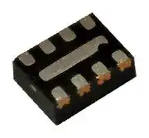


IP4254CZ8-4-TTL,13
EMI Filter, CRC PI Filter, ESD Protection, 4 Data Lines, DFN-8
- Manufacturer: NEXPERIA
- Product type: Integrated Passive Filters
- SVHC: No SVHC (21-Jan-2025)
- No. of Pins: 8Pins
- Product Range: IP4254 Series
- Filter Circuit: C-R-C Pi Filter
- EMI Filter Type: EMI Filter with ESD Protection
- No. of Data Lines: 4 Data Lines
- Filter Case / Package: DFN
| Delivery and price | |
|---|---|
| Units per pack | 10 |
| Price | 0.22 € |
| Current stock | 1000+ |
| Lead time | 7 days |
## **Important notice**

Dear Customer,

On 7 February 2017 the former NXP Standard Product business became a new company with the tradename **Nexperia** . Nexperia is an industry leading supplier of Discrete, Logic and PowerMOS semiconductors with its focus on the automotive, industrial, computing, consumer and wearable application markets

In data sheets and application notes which still contain NXP or Philips Semiconductors references, use the references to Nexperia, as shown below.

Instead of http://www.nxp.com, http://www.philips.com/ or http://www.semiconductors.philips.com/, use **http://www.nexperia.com**

Instead of sales.addresses@www.nxp.com or sales.addresses@www.semiconductors.philips.com, use **salesaddresses@nexperia.com** (email)

Replace the copyright notice at the bottom of each page or elsewhere in the document, depending on the version, as shown below:

- © NXP N.V. (year). All rights reserved or © Koninklijke Philips Electronics N.V. (year). All rights reserved

Should be replaced with:

- **© Nexperia B.V. (year). All rights reserved** .

If you have any questions related to the data sheet, please contact our nearest sales office via e-mail or telephone (details via **salesaddresses@nexperia.com** ). Thank you for your cooperation and understanding,

Kind regards,

Team Nexperia

## **IP4251/52/53/54-TTL**

**Integrated 4-, 6- and 8-channel passive filter network with ESD protection**

**Rev. 2 — 5 May 2011**

**Product data sheet**

## **1. Product profile**

## **1.1 General description**

The devices are 4-, 6- and 8-channel RC low-pass filter arrays which are designed to provide filtering of undesired RF signals on the I/O ports of portable communication or computing devices. In addition, the devices incorporate diodes to provide protection to downstream components from ElectroStatic Discharge (ESD) voltages as high as ±30 kV.

The devices are fabricated using monolithic silicon technology and integrate up to eight resistors and sixteen diodes in a 0.4 mm pitch 8-, 12- or 16-pin ultra-thin leadless Quad Flat No-leads (QFN) plastic package with a height of 0.55 mm only.

## **1.2 Features and benefits**

- Pb-free, Restriction of Hazardous Substances (RoHS) compliant and free of halogen and antimony (Dark Green compliant)

- 4-, 6- and 8-channel integrated π-type RC filter network

- ESD protection to ±30 kV contact discharge according to IEC 61000-4-2 far exceeding level 4

- QFN plastic package with 0.4 mm pitch and 0.55 mm height

## **1.3 Applications**

General-purpose ElectroMagnetic Interference (EMI) and Radio-Frequency Interference (RFI) filtering and downstream ESD protection for:

- Cellular phone and Personal Communication System (PCS) mobile handsets

- Cordless telephones

- Wireless data (WAN/LAN) systems

- Mobile Internet Devices (MID)

- Portable Media Players (PMP)

**==> picture [172 x 101] intentionally omitted <==**

**IP4251/52/53/54-TTL**

**NXP Semiconductors**

**Integrated 4-, 6- and 8-channel passive filter network**

## **1.4 Quick reference data**

|**Table 1.**|**Quick reference data**|||||||
|---|---|---|---|---|---|---|---|
|**Symbol**|**Parameter**|**Conditions**||**Min**|**Typ**|**Max**|**Unit**|
|**IP4251CZ8-4-TTL; IP4251CZ12-6-TTL; IP4251CZ16-8-TTL**||||||||
|Cch|channel capacitance|f = 100 kHz;|[1]|-|10|-|pF|
|||Vbias(DC)= 2.5 V||||||
|Rs(ch)|channel series resistance|||80|100|120|Ω|
|**IP4252CZ8-4-TTL; IP4252CZ12-6-TTL; IP4252CZ16-8-TTL**||||||||
|Cch|channel capacitance|f = 100 kHz;|[1]|-|12|-|pF|
|||Vbias(DC)= 2.5 V||||||
|Rs(ch)|channel series resistance|||32|40|48|Ω|
|**IP4253CZ8-4-TTL; IP4253CZ12-6-TTL; IP4253CZ16-8-TTL**||||||||
|Cch|channel capacitance|f = 100 kHz;|[1]|-|30|-|pF|
|||Vbias(DC)= 2.5 V||||||
|Rs(ch)|channel series resistance|||160|200|240|Ω|
|**IP4254CZ8-4-TTL; IP4254CZ12-6-TTL; IP4254CZ16-8-TTL**||||||||
|Cch|channel capacitance|f = 100 kHz;|[1]|-|30|-|pF|
|||Vbias(DC)= 2.5 V||||||
|Rs(ch)|channel series resistance|||80|100|120|Ω|


[1] For the total channel.

## **2. Pinning information**

## **Table 2. Pinning**

|**Pin**<br>**Description**<br>**Simplified outline**<br>**Graphic symbol**|**Pin**<br>**Description**<br>**Simplified outline**<br>**Graphic symbol**|
|---|---|
|**IP4251CZ8-4-TTL; IP4252CZ8-4-TTL; IP4253CZ8-4-TTL; IP4254CZ8-4-TTL (SOT1166-1)**||
|1 and 8<br>filter channel 1<br>2 and 7<br>filter channel 2<br>3 and 6<br>filter channel 3<br>4 and 5<br>filter channel 4<br>ground pad<br>ground<br>Transparent<br>top view<br>8<br>1<br>5<br>4<br>1 to 4|_018aaa071_<br>Rs(ch)<br>Cch<br>5 to 8<br>GND<br>2<br>Cch<br>2|


**==> picture [396 x 115] intentionally omitted <==**

**----- Start of picture text -----**<br>
IP4251CZ12-6-TTL; IP4252CZ12-6-TTL; IP4253CZ12-6-TTL; IP4254CZ12-6-TTL (SOT1167-1)<br>1 and 12 filter channel 1<br>12 7 Rs(ch)<br>2 and 11 filter channel 2 1 to 6 7 to 12<br>3 and 10 filter channel 3 Cch Cch<br>2 2<br>4 and 9 filter channel 4 1 6<br>5 and 8 filter channel 5 Transparent<br>top view GND<br>6 and 7 filter channel 6 018aaa072<br>ground pad ground<br>**----- End of picture text -----**<br>


All information provided in this document is subject to legal disclaimers. © NXP B.V. 2011. All rights reserved.

IP4251_52_53_54-TTL **Product data sheet**

**Rev. 2 — 5 May 2011**

**2 of 18**

**IP4251/52/53/54-TTL**

**NXP Semiconductors**

**Integrated 4-, 6- and 8-channel passive filter network**

**Table 2. Pinning** _…continued_

|**Pin**<br>**Description**<br>**Simplified outline**<br>**Graphic symbol**|**Pin**<br>**Description**<br>**Simplified outline**<br>**Graphic symbol**|
|---|---|
|**IP4251CZ16-8-TTL; IP4252CZ16-8-TTL; IP4253CZ16-8-TTL; IP4254CZ16-8-TTL (SOT1168-1)**||
|1 and 16<br>filter channel 1<br>2 and 15<br>filter channel 2<br>3 and 14<br>filter channel 3<br>4 and 13<br>filter channel 4<br>5 and 12<br>filter channel 5<br>6 and 11<br>filter channel 6<br>7 and 10<br>filter channel 7<br>8 and 9<br>filter channel 8<br>ground pad<br>ground<br>Transparent<br>top view<br>16<br>1<br>9<br>8<br>1 to 8|_018aaa073_<br>Rs(ch)<br>9 to 16<br>GND<br>Cch<br>2<br>Cch<br>2|


## **3. Ordering information**

**Table 3. Ordering information**

|**Type number**|**Package**|**Package**|**Package**|
|---|---|---|---|
||**Name**|**Description**|**Version**|
|IP4251CZ8-4-TTL|HUSON8<br>plastic, thermal enhanced ultra thin small outline package; no leads;<br>8 terminals; body 1.35×1.7×0.55 mm<br>SOT1166-1|||
|IP4251CZ12-6-TTL|HUSON12<br>plastic, thermal enhanced ultra thin small outline package; no leads;<br>12 terminals; body 1.35×2.5×0.55 mm<br>SOT1167-1|||
|IP4251CZ16-8-TTL|HUSON16<br>plastic, thermal enhanced ultra thin small outline package; no leads;<br>16 terminals; body 1.35×3.3×0.55 mm<br>SOT1168-1|||
|IP4252CZ8-4-TTL|HUSON8<br>plastic, thermal enhanced ultra thin small outline package; no leads;<br>8 terminals; body 1.35×1.7×0.55 mm<br>SOT1166-1|||
|IP4252CZ12-6-TTL|HUSON12<br>plastic, thermal enhanced ultra thin small outline package; no leads;<br>12 terminals; body 1.35×2.5×0.55 mm<br>SOT1167-1|||
|IP4252CZ16-8-TTL|HUSON16<br>plastic, thermal enhanced ultra thin small outline package; no leads;<br>16 terminals; body 1.35×3.3×0.55 mm<br>SOT1168-1|||
|IP4253CZ8-4-TTL|HUSON8<br>plastic, thermal enhanced ultra thin small outline package; no leads;<br>8 terminals; body 1.35×1.7×0.55 mm<br>SOT1166-1|||
|IP4253CZ12-6-TTL|HUSON12<br>plastic, thermal enhanced ultra thin small outline package; no leads;<br>12 terminals; body 1.35×2.5×0.55 mm<br>SOT1167-1|||
|IP4253CZ16-8-TTL|HUSON16<br>plastic, thermal enhanced ultra thin small outline package; no leads;<br>16 terminals; body 1.35×3.3×0.55 mm<br>SOT1168-1|||
|IP4254CZ8-4-TTL|HUSON8<br>plastic, thermal enhanced ultra thin small outline package; no leads;<br>8 terminals; body 1.35×1.7×0.55 mm<br>SOT1166-1|||
|IP4254CZ12-6-TTL|HUSON12<br>plastic, thermal enhanced ultra thin small outline package; no leads;<br>12 terminals; body 1.35×2.5×0.55 mm<br>SOT1167-1|||
|IP4254CZ16-8-TTL|HUSON16<br>plastic, thermal enhanced ultra thin small outline package; no leads;<br>16 terminals; body 1.35×3.3×0.55 mm<br>SOT1168-1|||


© NXP B.V. 2011. All rights reserved.

All information provided in this document is subject to legal disclaimers.

IP4251_52_53_54-TTL **Product data sheet**

**Rev. 2 — 5 May 2011**

**3 of 18**

**IP4251/52/53/54-TTL**

**NXP Semiconductors**

**Integrated 4-, 6- and 8-channel passive filter network**

## **4. Limiting values**

## **Table 4. Limiting values**

_In accordance with the Absolute Maximum Rating System (IEC 60134)._

|**Symbol**<br>**Parameter**<br>**Conditions**<br>**Min**<br>**Max**<br>**Unit**|**Symbol**<br>**Parameter**<br>**Conditions**<br>**Min**<br>**Max**<br>**Unit**|
|---|---|
|**IP4251CZ8-4-TTL; IP4251CZ12-6-TTL; IP4251CZ16-8-TTL**||
|VESD<br>electrostatic discharge<br>voltage<br>all pins to ground;<br>contact discharge<br>[1]<br>-<br>±15<br>kV||
|**IP4252CZ8-4-TTL; IP4252CZ12-6-TTL; IP4252CZ16-8-TTL**||
|VESD<br>electrostatic discharge<br>voltage<br>all pins to ground;<br>contact discharge<br>[1]<br>-<br>±15<br>kV||
|**IP4253CZ8-4-TTL; IP4253CZ12-6-TTL; IP4253CZ16-8-TTL**||
|VESD<br>electrostatic discharge<br>voltage|all pins to ground<br>[2]|
||contact discharge<br>-<br>±30<br>kV|
||air discharge<br>-<br>±30<br>kV|
|**IP4254CZ8-4-TTL; IP4254CZ12-6-TTL; IP4254CZ16-8-TTL**||
|VESD<br>electrostatic discharge<br>voltage|all pins to ground<br>[2]|
||contact discharge<br>-<br>±30<br>kV|
||air discharge<br>-<br>±30<br>kV|
|**Per device**||
|VESD<br>electrostatic discharge<br>voltage|IEC 61000-4-2, level 4;<br>all pins to ground|
||contact discharge<br>-<br>±8<br>kV|
||air discharge<br>-<br>±15<br>kV|
|VCC<br>supply voltage|−0.5<br>+5.6<br>V|
|Pch<br>channel power dissipation|Tamb= 85°C<br>-<br>60<br>mW|
|Ptot<br>total power dissipation|Tamb= 85°C<br>-<br>200<br>mW|
|Tstg<br>storage temperature|−55<br>+150<br>°C|
|Tamb<br>ambient temperature|−40<br>+85<br>°C|


[1] Device tested with 1000 pulses of ±15 kV contact discharges, according to the IEC 61000-4-2 model, far exceeding IEC 61000-4-2 level 4 (8 kV contact discharge).

[2] Device tested with 1000 pulses of ±30 kV contact discharges, according to the IEC 61000-4-2 model, far exceeding IEC 61000-4-2 level 4 (8 kV contact discharge).

All information provided in this document is subject to legal disclaimers. © NXP B.V. 2011. All rights reserved.

IP4251_52_53_54-TTL **Product data sheet**

**Rev. 2 — 5 May 2011**

**4 of 18**

**IP4251/52/53/54-TTL**

**NXP Semiconductors**

**Integrated 4-, 6- and 8-channel passive filter network**

## **5. Characteristics**

## **Table 5. Channel characteristics**

_Tamb = 25_ ° _C unless otherwise specified._

|**Symbol**<br>**Parameter**<br>**Conditions**<br>**Min**<br>**Typ**<br>**Max**<br>**Unit**|**Symbol**<br>**Parameter**<br>**Conditions**<br>**Min**<br>**Typ**<br>**Max**<br>**Unit**|
|---|---|
|**IP4251CZ8-4-TTL; IP4251CZ12-6-TTL; IP4251CZ16-8-TTL**||
|Cch<br>channel capacitance|f = 100 kHz<br>[1]|
||Vbias(DC)= 2.5 V<br>-<br>10<br>-<br>pF|
||Vbias(DC)= 0 V<br>[2]<br>-<br>15<br>-<br>pF|
|Rs(ch)<br>channel series resistance|80<br>100<br>120<br>Ω|
|**IP4252CZ8-4-TTL; IP4252CZ12-6-TTL; IP4252CZ16-8-TTL**||
|Cch<br>channel capacitance|f = 100 kHz<br>[1]|
||Vbias(DC)= 2.5 V<br>-<br>12<br>-<br>pF|
||Vbias(DC)= 0 V<br>[2]<br>-<br>18<br>-<br>pF|
|Rs(ch)<br>channel series resistance|32<br>40<br>48<br>Ω|
|**IP4253CZ8-4-TTL; IP4253CZ12-6-TTL; IP4253CZ16-8-TTL**||
|Cch<br>channel capacitance|f = 100 kHz<br>[1]|
||Vbias(DC)= 2.5 V<br>-<br>30<br>-<br>pF|
||Vbias(DC)= 0 V<br>[2]<br>-<br>45<br>-<br>pF|
|Rs(ch)<br>channel series resistance|160<br>200<br>240<br>Ω|
|**IP4254CZ8-4-TTL; IP4254CZ12-6-TTL; IP4254CZ16-8-TTL**||
|Cch<br>channel capacitance|f = 100 kHz<br>[1]|
||Vbias(DC)= 2.5 V<br>-<br>30<br>-<br>pF|
||Vbias(DC)= 0 V<br>[2]<br>-<br>45<br>-<br>pF|
|Rs(ch)<br>channel series resistance|80<br>100<br>120<br>Ω|
|**Per device**||
|ILR<br>reverse leakage current|per channel; VI= 3.5 V<br>-<br>-<br>0.1<br>μA|
|VBR<br>breakdown voltage|positive clamp; II= 1 mA<br>5.8<br>-<br>9<br>V|
|VF<br>forward voltage|negative clamp; IF= 1 mA<br>0.4<br>-<br>1.5<br>V|


[1] For the total channel.

[2] Guaranteed by design.

© NXP B.V. 2011. All rights reserved.

All information provided in this document is subject to legal disclaimers.

IP4251_52_53_54-TTL

**Product data sheet**

**Rev. 2 — 5 May 2011**

**5 of 18**

**IP4251/52/53/54-TTL**

**NXP Semiconductors**

**Integrated 4-, 6- and 8-channel passive filter network**

**Table 6. Frequency characteristics** _Tamb = 25_ ° _C unless otherwise specified._

|**Symbol**<br>**Parameter**<br>**Conditions**<br>**Min**<br>**Typ**<br>**Max**<br>**Unit**|**Symbol**<br>**Parameter**<br>**Conditions**<br>**Min**<br>**Typ**<br>**Max**<br>**Unit**|
|---|---|
|**IP4251CZ8-4-TTL; IP4251CZ12-6-TTL; IP4251CZ16-8-TTL**||
|αil<br>insertion loss|Rsource= 50Ω; RL= 50Ω|
||800 MHz < f < 3 GHz<br>-<br>16<br>-<br>dB|
||f = 1 GHz<br>-<br>20<br>-<br>dB|
|αct<br>crosstalk attenuation|Rsource= 50Ω; RL= 50Ω;<br>800 MHz < f < 3 GHz<br>-<br>30<br>-<br>dB|
|**IP4252CZ8-4-TTL; IP4252CZ12-6-TTL; IP4252CZ16-8-TTL**||
|αil<br>insertion loss|Rsource= 50Ω; RL= 50Ω|
||800 MHz < f < 3 GHz<br>-<br>12<br>-<br>dB|
||f = 1 GHz<br>-<br>14<br>-<br>dB|
|αct<br>crosstalk attenuation|Rsource= 50Ω; RL= 50Ω;<br>800 MHz < f < 3 GHz<br>-<br>40<br>-<br>dB|
|**IP4253CZ8-4-TTL; IP4253CZ12-6-TTL; IP4253CZ16-8-TTL**||
|αil<br>insertion loss|Rsource= 50Ω; RL= 50Ω|
||800 MHz < f < 3 GHz<br>-<br>33<br>-<br>dB|
||f = 1 GHz<br>35<br>-<br>-<br>dB|
|αct<br>crosstalk attenuation|Rsource= 50Ω; RL= 50Ω;<br>800 MHz < f < 3 GHz<br>-<br>30<br>-<br>dB|
|**IP4254CZ8-4-TTL; IP4254CZ12-6-TTL; IP4254CZ16-8-TTL**||
|αil<br>insertion loss|Rsource= 50Ω; RL= 50Ω|
||800 MHz < f < 3 GHz<br>-<br>28<br>-<br>dB|
||f = 1 GHz<br>30<br>-<br>-<br>dB|
|αct<br>crosstalk attenuation|Rsource= 50Ω; RL= 50Ω;<br>800 MHz < f < 3 GHz<br>-<br>30<br>-<br>dB|


© NXP B.V. 2011. All rights reserved.

All information provided in this document is subject to legal disclaimers. **Rev. 2 — 5 May 2011**

IP4251_52_53_54-TTL

**Product data sheet**

**6 of 18**

**IP4251/52/53/54-TTL**

**NXP Semiconductors**

**Integrated 4-, 6- and 8-channel passive filter network**

## **6. Application information**

## **6.1 Insertion loss**

The devices are designed as EMI/RFI filters for multichannel interfaces.

The block schematic for measuring insertion loss in a 50 Ω system is shown in Figure 1. Typical measurements results are shown in Figure 2 to Figure 6 for the different devices.

**==> picture [497 x 281] intentionally omitted <==**

**----- Start of picture text -----**<br>
001aaj308<br>0<br>S21<br>(dB)<br>−10<br>(1)<br>(2)<br>(3)<br>−20 (4)<br>−30<br>DUT<br>IN OUT<br>50 Ω 50 Ω −40<br>Vgen<br>−50<br>10 [−][1] 1 10 10 [2] 10 [3] 10 [4]<br>018aaa074 f (MHz)<br>(1) IP4252CZ16-8-TTL - channel 1 to channel 16<br>(2) IP4251CZ16-8-TTL - channel 1 to channel 16<br>(3) IP4254CZ16-8-TTL - channel 1 to channel 16<br>(4) IP4253CZ16-8-TTL - channel 1 to channel 16<br>Fig 1. Frequency response setup Fig 2. Frequency response curves overview<br>**----- End of picture text -----**<br>


© NXP B.V. 2011. All rights reserved.

All information provided in this document is subject to legal disclaimers.

IP4251_52_53_54-TTL **Product data sheet**

**Rev. 2 — 5 May 2011**

**7 of 18**

**IP4251/52/53/54-TTL**

**NXP Semiconductors**

**Integrated 4-, 6- and 8-channel passive filter network**

**==> picture [481 x 189] intentionally omitted <==**

**----- Start of picture text -----**<br>
001aaj608 001aaj609<br>0 0<br>S21 S21<br>(dB) (dB)<br>−10 −10<br>(1)<br>−20 (2) −20<br>(1)<br>−30 −30 (2)<br>−40 −40<br>−50 −50<br>10 [−][1] 1 10 10 [2] 10 [3] 10 [4] 10 [−][1] 1 10 10 [2] 10 [3] 10 [4]<br>f (MHz) f (MHz)<br>**----- End of picture text -----**<br>


- (1) Channel 1 to channel 16

- (2) Channel 4 to channel 13

**Fig 3. IP4251CZ16-8-TTL: frequency response curves**

- (1) Channel 1 to channel 16

(2) Channel 4 to channel 13 **Fig 4. IP4252CZ16-8-TTL: frequency response curves**

**==> picture [482 x 247] intentionally omitted <==**

**----- Start of picture text -----**<br>
001aaj610 001aaj611<br>0 0<br>S21 S21<br>(dB) (dB)<br>−10 −10<br>−20 −20<br>−30 (1) −30 (1)(2)<br>(2)<br>−40 −40<br>−50 −50<br>10 [−][1] 1 10 10 [2] 10 [3] 10 [4] 10 [−][1] 1 10 10 [2] 10 [3] 10 [4]<br>f (MHz) f (MHz)<br>(1) Channel 1 to channel 16 (1) Channel 4 to channel 13<br>(2) Channel 4 to channel 13 (2) Channel 1 to channel 16<br>Fig 5. IP4253CZ16-8-TTL: frequency response  Fig 6. IP4254CZ16-8-TTL: frequency response<br>curves curves<br>**----- End of picture text -----**<br>


Due to the optimized silicon dice and package design, all channels in a single package show a very good matching performance as the insertion loss for a channel at the package side (e.g. channel 1 to channel 16) is nearly identical with the center channels (e.g. channel 4 to channel 13).

© NXP B.V. 2011. All rights reserved.

All information provided in this document is subject to legal disclaimers.

IP4251_52_53_54-TTL

**Product data sheet**

**Rev. 2 — 5 May 2011**

**8 of 18**

**IP4251/52/53/54-TTL**

**NXP Semiconductors**

**Integrated 4-, 6- and 8-channel passive filter network**

## **6.2 Selection**

The selection of one of the filter devices has to be performed depending on the maximum clock frequency, driver strength, capacitive load of the sink, and also the maximum applicable rise and fall times.

## **6.2.1 SDHC and MMC memory interface**

The Secure Digital High Capacity (SDHC) memory card interface standard specification and the Multi Media Card (MMC) (JESD 84A43) standard specification recommend a rise and fall time of 25 % to 62.5 % (62.5 % to 25 % respectively) of 3 ns or less for the input signal of the receiving interface side.

Assuming a typical capacitance of about 20 pF for the SDHC memory card itself, and approximately 4 pF to 7 pF for the Printed-Circuit Board (PCB) and the card holder, IP4252CZ12-6-TTL (6 channels, Rs(ch) = 40 Ω, Cch = 12 pF at Vbias(DC) = 2.5 V) is a matching selection to filter and protect all relevant interface pins such as CLK, CMD, and DAT0 to DAT3/CD. Please refer to Figure 7 for a general example of the implementation of the device in an SDHC card interface.

In case additional channels such as write-protect or a mechanical card-detection switch are used, the IP4252CZ16-8-TTL (8 channels, Rs(ch) = 40 Ω, Cch = 12 pF at Vbias(DC) = 2.5 V) offers two additional channels.

© NXP B.V. 2011. All rights reserved.

All information provided in this document is subject to legal disclaimers.

IP4251_52_53_54-TTL **Product data sheet**

**Rev. 2 — 5 May 2011**

**9 of 18**

**IP4251/52/53/54-TTL**

**NXP Semiconductors**

**Integrated 4-, 6- and 8-channel passive filter network**

**==> picture [371 x 358] intentionally omitted <==**

**----- Start of picture text -----**<br>
to HOST VCC(VSD)<br>INTERFACE<br>DAT3/CD pull-up pull-up resistors<br>10 kΩ − 100 kΩ 10 kΩ − 100 kΩ<br>IP4252CZ12-6-TTL<br>(IP4252CZ16-8-TTL)<br>DAT1 DAT1 SD MEMORY<br>DAT0 DAT0 CARD<br>CLK GND SET_CLR_<br>CMD CLK CARD_DETECT<br>DAT3/CD VCC(VSD) (ACMD42)<br>DAT2 CMD 10 kΩ − 90 kΩ<br>CD DAT3/CD<br>WP DAT2<br>DAT3/CD pull-up optional:<br>>270 kΩ 2-additional channels<br>exact value of IP4252CZ16-8-TTL<br>depends on<br>required<br>logic levels<br>optional:<br>electrical card detect<br>CD<br>WP optional:<br>card detect switch<br>optional:<br>write protect switch 018aaa075<br>**----- End of picture text -----**<br>


**==> picture [228 x 10] intentionally omitted <==**

**----- Start of picture text -----**<br>
Fig 7. Example of IP4252 in an SDHC card interface<br>**----- End of picture text -----**<br>


The capacitance values specified for the signal channels of the MMC interface differ from the SDHC specification. The MMC card-side interface is specified to have an intrinsic capacitance of 12 pF to 18 pF and the total channel is limited according to the specification to 30 pF only. Therefore, any filter device capacitance is limited to a maximum of up to 18 pF, including the card holder and PCB traces.

Please refer to Figure 8 for a general example of the implementation of the IP4252 in an MMC interface application.

© NXP B.V. 2011. All rights reserved.

All information provided in this document is subject to legal disclaimers.

IP4251_52_53_54-TTL **Product data sheet**

**Rev. 2 — 5 May 2011**

**10 of 18**

**IP4251/52/53/54-TTL**

**NXP Semiconductors**

**Integrated 4-, 6- and 8-channel passive filter network**

**==> picture [377 x 267] intentionally omitted <==**

**----- Start of picture text -----**<br>
VCC(VMMC)<br>CMD pull-up pull-up resistors<br>4.7 kΩ - 100 kΩ 50 kΩ - 100 kΩ<br>IP4252CZ12-6-TTL<br>DAT1 DAT1<br>C8<br>DAT0 DAT0<br>C7<br>DAT7 DAT7<br>C13<br>DAT6 VSS2<br>C6<br>CLK DAT6<br>C12<br>DAT5 CLK<br>C5<br>VCC(VMMC)<br>HOST C4<br>INTERFACE e.g.<br>VSS1 RSMMC<br>C3<br>DAT5<br>C11<br>CMD CMD<br>C2<br>DAT4 DAT4<br>C10<br>DAT3 DAT3<br>C1<br>DAT2 DAT2<br>C9<br>IP4252CZ8-4-TTL 018aaa076<br>Fig 8. Example of IP4252 in an MMC interface<br>**----- End of picture text -----**<br>


To generate SDHC and MMC-compliant digital signals, the driver strength should not significantly undercut 8 mA.

## **6.2.2 LCD interfaces, medium-speed interfaces**

For digital interfaces such as LCD interfaces running at clock speeds between 10 MHz and 25 MHz or more, IP4251, IP4252 or IP4254 can be used depending on the sink load, clock speed, driver strength and rise and fall time requirements. Also the minimum EMI filter requirements may be a decision-making factor.

## **6.2.3 Keypad, low-speed interfaces**

Especially for lower-speed interfaces such as keypads, low-speed serial interfaces (e.g. Recommended Standard (RS) 232) and low-speed control signals, IP4253 (Rs(ch) = 200 Ω, Cch = 30 pF at Vbias(DC) = 2.5 V) offers a very robust ESD protection and strong suppression of unwanted frequencies (EMI filtering).

© NXP B.V. 2011. All rights reserved.

All information provided in this document is subject to legal disclaimers.

IP4251_52_53_54-TTL **Product data sheet**

**Rev. 2 — 5 May 2011**

**11 of 18**

**IP4251/52/53/54-TTL**

**NXP Semiconductors**

**Integrated 4-, 6- and 8-channel passive filter network**

## **7. Package outline**

**==> picture [481 x 18] intentionally omitted <==**

**----- Start of picture text -----**<br>
HUSON8: plastic, thermal enhanced ultra thin small outline package; no leads;<br>8 terminals; body 1.35 x 1.7 x 0.55 mm SOT1166-1<br>**----- End of picture text -----**<br>


**==> picture [481 x 556] intentionally omitted <==**

**----- Start of picture text -----**<br>
X<br>D B A<br>E A<br>A1<br>c<br>terminal 1<br>index area<br>detail X<br>e1<br>C<br>terminal 1 e v C A B<br>index area b<br>w C y1 C y<br>1 4<br>L<br>k<br>Eh<br>8 5<br>Dh tiebars are indicated on<br>arbitrary location and size<br>0 1 2 mm<br>scale<br>Dimensions<br>Unit [(1)] A A1 b c D Dh E Eh e e1 k L v w y y1<br>max 0.55 0.05 0.25 1.8 1.3 1.45 0.45 0.30<br>mm nom 0.20 0.127 1.7 1.2 1.35 0.40 0.4 1.2 0.25 0.1 0.05 0.05 0.05<br>min 0.00 0.15 1.6 1.1 1.25 0.35 0.2 0.20<br>Note<br>1. Plastic or metal protrusions of 0.075 mm maximum per side are not included. sot1166-1_po<br>Outline References European Issue date<br>version IEC JEDEC JEITA projection<br>10-03-18<br>SOT1166-1 - - - - - - - - - 10-03-22<br>**----- End of picture text -----**<br>


**Fig 9. Package outline SOT1166-1 (HUSON8)**

All information provided in this document is subject to legal disclaimers.

© NXP B.V. 2011. All rights reserved.

IP4251_52_53_54-TTL

**Product data sheet**

**Rev. 2 — 5 May 2011**

**12 of 18**

**IP4251/52/53/54-TTL**

**NXP Semiconductors**

**Integrated 4-, 6- and 8-channel passive filter network**

**HUSON12: plastic, thermal enhanced ultra thin small outline package; no leads; 12 terminals; body 1.35 x 2.5 x 0.55 mm SOT1167-1**

**==> picture [481 x 556] intentionally omitted <==**

**----- Start of picture text -----**<br>
X<br>D B A<br>E A<br>A1<br>c<br>terminal 1<br>index area<br>detail X<br>e1<br>C<br>terminal 1 e v C A B<br>index area b<br>w C y1 C y<br>1 6<br>L<br>k<br>Eh<br>12 7<br>Dh tiebars are indicated on<br>arbitrary location and size<br>0 1 2 mm<br>scale<br>Dimensions<br>Unit [(1)] A A1 b c D Dh E Eh e e1 k L v w y y1<br>max 0.55 0.05 0.25 2.6 2.1 1.45 0.45 0.30<br>mm nom 0.20 0.127 2.5 2.0 1.35 0.40 0.4 2.0 0.25 0.1 0.05 0.05 0.05<br>min 0.00 0.15 2.4 1.9 1.25 0.35 0.2 0.20<br>Note<br>1. Plastic or metal protrusions of 0.075 mm maximum per side are not included. sot1167-1_po<br>Outline References European Issue date<br>version IEC JEDEC JEITA projection<br>10-03-18<br>SOT1167-1 - - - - - - - - - 10-03-22<br>**----- End of picture text -----**<br>


## **Fig 10. Package outline SOT1167-1 (HUSON12)**

All information provided in this document is subject to legal disclaimers.

© NXP B.V. 2011. All rights reserved.

IP4251_52_53_54-TTL

**Product data sheet**

**Rev. 2 — 5 May 2011**

**13 of 18**

**IP4251/52/53/54-TTL**

**NXP Semiconductors**

**Integrated 4-, 6- and 8-channel passive filter network**

**HUSON16: plastic, thermal enhanced ultra thin small outline package; no leads; 16 terminals; body 1.35 x 3.3 x 0.55 mm**

**==> picture [42 x 7] intentionally omitted <==**

**----- Start of picture text -----**<br>
SOT1168-1<br>**----- End of picture text -----**<br>


**==> picture [481 x 556] intentionally omitted <==**

**----- Start of picture text -----**<br>
X<br>D B A<br>E A<br>A1<br>c<br>terminal 1<br>index area<br>detail X<br>e1<br>C<br>terminal 1 e v C A B<br>index area b<br>w C y1 C y<br>1 8<br>L<br>k<br>Eh<br>16 9<br>Dh tiebars are indicated on<br>arbitrary location and size<br>0 1 2 mm<br>scale<br>Dimensions<br>Unit [(1)] A A1 b c D Dh E Eh e e1 k L v w y y1<br>max 0.55 0.05 0.25 3.4 2.9 1.45 0.45 0.30<br>mm nom 0.20 0.127 3.3 2.8 1.35 0.40 0.4 2.8 0.25 0.1 0.05 0.05 0.05<br>min 0.00 0.15 3.2 2.7 1.25 0.35 0.2 0.20<br>Note<br>1. Plastic or metal protrusions of 0.075 mm maximum per side are not included. sot1168-1_po<br>Outline References European Issue date<br>version IEC JEDEC JEITA projection<br>10-03-18<br>SOT1168-1 - - - - - - - - - 10-03-22<br>**----- End of picture text -----**<br>


## **Fig 11. Package outline SOT1168-1 (HUSON16)**

All information provided in this document is subject to legal disclaimers.

© NXP B.V. 2011. All rights reserved.

IP4251_52_53_54-TTL

**Product data sheet**

**Rev. 2 — 5 May 2011**

**14 of 18**

**IP4251/52/53/54-TTL**

**NXP Semiconductors**

**Integrated 4-, 6- and 8-channel passive filter network**

## **8. Revision history**

|**Table 7.**<br>**Revision history**|**Table 7.**<br>**Revision history**||||
|---|---|---|---|---|
|**Document ID**|**Release date**|**Data sheet status**|**Change notice**|**Supersedes**|
|IP4251_52_53_54-TTL v.2|20110505|Product data sheet|-|IP4251_52_53_54-TTL v.1|
|Modifications:|**•** Section 1|“<br>Product profile<br>”<br>:updated.|||
||**•** Table 2“<br>Pinning<br>”<br>:updated.||||
||**•** Deleted section “Thermal characteristics”.||||
|IP4251_52_53_54-TTL v.1|20110131|Objective data sheet|-|-|


© NXP B.V. 2011. All rights reserved.

All information provided in this document is subject to legal disclaimers. **Rev. 2 — 5 May 2011**

IP4251_52_53_54-TTL **Product data sheet**

**15 of 18**

**IP4251/52/53/54-TTL**

**NXP Semiconductors**

**Integrated 4-, 6- and 8-channel passive filter network**

## **9. Legal information**

## **9.1 Data sheet status**

|**Document status[1]**<br>**[2]**|**Product statu**~~**s**~~**[3]**|**Definition**|
|---|---|---|
|Objective [short] data sheet|Development|This document contains data from the objective specification for product development.|
|Preliminary [short] data sheet|Qualification|This document contains data from the preliminary specification.|
|Product [short] data sheet|Production|This document contains the product specification.|


[1] Please consult the most recently issued document before initiating or completing a design.

[2] The term ‘short data sheet’ is explained in section “Definitions”.

[3] The product status of device(s) described in this document may have changed since this document was published and may differ in case of multiple devices. The latest product status information is available on the Internet at URL http://www.nxp.com.

## **9.2 Definitions**

**Draft —** The document is a draft version only. The content is still under internal review and subject to formal approval, which may result in modifications or additions. NXP Semiconductors does not give any representations or warranties as to the accuracy or completeness of information included herein and shall have no liability for the consequences of use of such information.

**Short data sheet —** A short data sheet is an extract from a full data sheet with the same product type number(s) and title. A short data sheet is intended for quick reference only and should not be relied upon to contain detailed and full information. For detailed and full information see the relevant full data sheet, which is available on request via the local NXP Semiconductors sales office. In case of any inconsistency or conflict with the short data sheet, the full data sheet shall prevail.

**Product specification —** The information and data provided in a Product data sheet shall define the specification of the product as agreed between NXP Semiconductors and its customer, unless NXP Semiconductors and customer have explicitly agreed otherwise in writing. In no event however, shall an agreement be valid in which the NXP Semiconductors product is deemed to offer functions and qualities beyond those described in the Product data sheet.

## **9.3 Disclaimers**

**Limited warranty and liability —** Information in this document is believed to be accurate and reliable. However, NXP Semiconductors does not give any representations or warranties, expressed or implied, as to the accuracy or completeness of such information and shall have no liability for the consequences of use of such information.

In no event shall NXP Semiconductors be liable for any indirect, incidental, punitive, special or consequential damages (including - without limitation - lost profits, lost savings, business interruption, costs related to the removal or replacement of any products or rework charges) whether or not such damages are based on tort (including negligence), warranty, breach of contract or any other legal theory.

Notwithstanding any damages that customer might incur for any reason whatsoever, NXP Semiconductors’ aggregate and cumulative liability towards customer for the products described herein shall be limited in accordance with the _Terms and conditions of commercial sale_ of NXP Semiconductors.

**Right to make changes —** NXP Semiconductors reserves the right to make changes to information published in this document, including without limitation specifications and product descriptions, at any time and without notice. This document supersedes and replaces all information supplied prior to the publication hereof.

**Suitability for use —** NXP Semiconductors products are not designed, authorized or warranted to be suitable for use in life support, life-critical or safety-critical systems or equipment, nor in applications where failure or

malfunction of an NXP Semiconductors product can reasonably be expected to result in personal injury, death or severe property or environmental damage. NXP Semiconductors accepts no liability for inclusion and/or use of NXP Semiconductors products in such equipment or applications and therefore such inclusion and/or use is at the customer’s own risk.

**Applications —** Applications that are described herein for any of these products are for illustrative purposes only. NXP Semiconductors makes no representation or warranty that such applications will be suitable for the specified use without further testing or modification.

Customers are responsible for the design and operation of their applications and products using NXP Semiconductors products, and NXP Semiconductors accepts no liability for any assistance with applications or customer product design. It is customer’s sole responsibility to determine whether the NXP Semiconductors product is suitable and fit for the customer’s applications and products planned, as well as for the planned application and use of customer’s third party customer(s). Customers should provide appropriate design and operating safeguards to minimize the risks associated with their applications and products.

NXP Semiconductors does not accept any liability related to any default, damage, costs or problem which is based on any weakness or default in the customer’s applications or products, or the application or use by customer’s third party customer(s). Customer is responsible for doing all necessary testing for the customer’s applications and products using NXP Semiconductors products in order to avoid a default of the applications and the products or of the application or use by customer’s third party customer(s). NXP does not accept any liability in this respect.

**Limiting values —** Stress above one or more limiting values (as defined in the Absolute Maximum Ratings System of IEC 60134) will cause permanent damage to the device. Limiting values are stress ratings only and (proper) operation of the device at these or any other conditions above those given in the Recommended operating conditions section (if present) or the Characteristics sections of this document is not warranted. Constant or repeated exposure to limiting values will permanently and irreversibly affect the quality and reliability of the device.

**Terms and conditions of commercial sale —** NXP Semiconductors products are sold subject to the general terms and conditions of commercial sale, as published at http://www.nxp.com/profile/terms, unless otherwise agreed in a valid written individual agreement. In case an individual agreement is concluded only the terms and conditions of the respective agreement shall apply. NXP Semiconductors hereby expressly objects to applying the customer’s general terms and conditions with regard to the purchase of NXP Semiconductors products by customer.

**No offer to sell or license —** Nothing in this document may be interpreted or construed as an offer to sell products that is open for acceptance or the grant, conveyance or implication of any license under any copyrights, patents or other industrial or intellectual property rights.

**Export control —** This document as well as the item(s) described herein may be subject to export control regulations. Export might require a prior authorization from national authorities.

IP4251_52_53_54-TTL All information provided in this document is subject to legal disclaimers. © NXP B.V. 2011. All rights reserved.

**Product data sheet**

**Rev. 2 — 5 May 2011**

**16 of 18**

**IP4251/52/53/54-TTL**

**NXP Semiconductors**

## **Integrated 4-, 6- and 8-channel passive filter network**

**Quick reference data —** The Quick reference data is an extract of the product data given in the Limiting values and Characteristics sections of this document, and as such is not complete, exhaustive or legally binding.

**Non-automotive qualified products —** Unless this data sheet expressly states that this specific NXP Semiconductors product is automotive qualified, the product is not suitable for automotive use. It is neither qualified nor tested in accordance with automotive testing or application requirements. NXP Semiconductors accepts no liability for inclusion and/or use of non-automotive qualified products in automotive equipment or applications.

In the event that customer uses the product for design-in and use in automotive applications to automotive specifications and standards, customer (a) shall use the product without NXP Semiconductors’ warranty of the

product for such automotive applications, use and specifications, and (b) whenever customer uses the product for automotive applications beyond NXP Semiconductors’ specifications such use shall be solely at customer’s own risk, and (c) customer fully indemnifies NXP Semiconductors for any liability, damages or failed product claims resulting from customer design and use of the product for automotive applications beyond NXP Semiconductors’ standard warranty and NXP Semiconductors’ product specifications.

## **9.4 Trademarks**

Notice: All referenced brands, product names, service names and trademarks are the property of their respective owners.

## **10. Contact information**

For more information, please visit: **http://www.nxp.com**

For sales office addresses, please send an email to: **salesaddresses@nxp.com**

© NXP B.V. 2011. All rights reserved.

All information provided in this document is subject to legal disclaimers.

IP4251_52_53_54-TTL

**Product data sheet**

**Rev. 2 — 5 May 2011**

**17 of 18**

**IP4251/52/53/54-TTL**

**NXP Semiconductors**

**Integrated 4-, 6- and 8-channel passive filter network**

## **11. Contents**

|**1**|**Product profile . . . . . . . . . . . . . . . . . . . . . . . . . .  1**|
|---|---|
|1.1|General description  . . . . . . . . . . . . . . . . . . . . .  1|
|1.2|Features and benefits. . . . . . . . . . . . . . . . . . . .  1|
|1.3|Applications  . . . . . . . . . . . . . . . . . . . . . . . . . . .  1|
|1.4|Quick reference data  . . . . . . . . . . . . . . . . . . . .  2|
|**2**|**Pinning information. . . . . . . . . . . . . . . . . . . . . .  2**|
|**3**|**Ordering information. . . . . . . . . . . . . . . . . . . . .  3**|
|**4**|**Limiting values. . . . . . . . . . . . . . . . . . . . . . . . . .  4**|
|**5**|**Characteristics. . . . . . . . . . . . . . . . . . . . . . . . . .  5**|
|**6**|**Application information. . . . . . . . . . . . . . . . . . .  7**|
|6.1|Insertion loss  . . . . . . . . . . . . . . . . . . . . . . . . . .  7|
|6.2|Selection. . . . . . . . . . . . . . . . . . . . . . . . . . . . . .  9|
|6.2.1|SDHC and MMC memory interface  . . . . . . . . .  9|
|6.2.2|LCD interfaces, medium-speed interfaces . . .  11|
|6.2.3|Keypad, low-speed interfaces. . . . . . . . . . . . .  11|
|**7**|**Package outline . . . . . . . . . . . . . . . . . . . . . . . .  12**|
|**8**|**Revision history. . . . . . . . . . . . . . . . . . . . . . . .  15**|
|**9**|**Legal information. . . . . . . . . . . . . . . . . . . . . . .  16**|
|9.1|Data sheet status . . . . . . . . . . . . . . . . . . . . . .  16|
|9.2|Definitions. . . . . . . . . . . . . . . . . . . . . . . . . . . .  16|
|9.3|Disclaimers . . . . . . . . . . . . . . . . . . . . . . . . . . .  16|
|9.4|Trademarks. . . . . . . . . . . . . . . . . . . . . . . . . . .  17|
|**10**|**Contact information. . . . . . . . . . . . . . . . . . . . .  17**|
|**11**|**Contents . . . . . . . . . . . . . . . . . . . . . . . . . . . . . .  18**|


Please be aware that important notices concerning this document and the product(s) described herein, have been included in section ‘Legal information’.

**© NXP B.V. 2011.**

**All rights reserved.**

For more information, please visit: http://www.nxp.com For sales office addresses, please send an email to: salesaddresses@nxp.com **Date of release: 5 May 2011 Document identifier: IP4251_52_53_54-TTL**
Updated at March 17, 2026
Nexperia is a dedicated global leader in discretes, logic, and MOSFET devices. Built on over half a century of semiconductor expertise and operating independently since 2017, the company produces consistently reliable components at an exceptional volume of 85 billion units annually. With its own manufacturing facilities, Nexperia delivers industry-leading small packages that combine power and thermal efficiency with best-in-class quality, meeting the rigorous standards of the automotive sector. Our extensive Nexperia portfolio is heavily focused on discrete semiconductors, providing engineers with a robust selection of core building blocks. This includes a comprehensive range of diodes and rectifiers, featuring a vast selection of Zener single diodes and Schottky diodes designed for precise voltage regulation and efficient power routing. Additionally, we offer an expansive array of bipolar transistors and single MOSFETs tailored for reliable switching and amplification in demanding applications. Beyond these primary offerings, the lineup extends into specialized circuit protection and passive components. This includes transient voltage suppressor (TVS) diodes, Zener array diodes, and small signal diodes, alongside dual MOSFETs and fast recovery rectifiers. For comprehensive design needs, the selection also encompasses integrated passive filters, common mode chokes, and precision timers and oscillators, ensuring a complete solution for high-performance electronic systems.
About Novapart
Novapart is a B2B electronic component broker specialising in stock shortages and cost reduction. We source hard-to-find parts and identify compliant alternatives across a catalogue of 410,000+ components from 500+ manufacturers.
Learn more →Stock Shortage Specialist
When a component is unavailable, discontinued or has an unacceptable lead time, we tap into our network of vetted European and Asian distributors to source what you need — without compromising on quality or traceability.
Request a quote →Compliant Alternatives
We identify pin-to-pin, electrically equivalent substitutes that meet the same certifications (RoHS, AEC-Q100, REACH) as your original specification — validated against datasheets, not just part numbers. Often at a lower cost.
BOM Analysis service →