
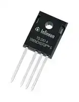


IKZ50N65NH5XKSA1
IGBT, 85 A, 1.65 V, 273 W, 650 V, TO-247, 4 Pins
- Manufacturer: INFINEON
- Product type: Single IGBTs
- No. of Pins: 4Pins
- Product Range: TRENCHSTOP 5
- Power Dissipation: 273W
- Transistor Mounting: Through Hole
- Transistor Case Style: TO-247
- Operating Temperature Max: 175°C
- Continuous Collector Current: 85A
- Collector Emitter Voltage Max: 650V
- Collector Emitter Saturation Voltage: 1.65V
| Delivery and price | |
|---|---|
| Units per pack | 1000 |
| Price | 3.44 € |
| Current stock | 10+ |
| Lead time | 30 days |
## IGBT
High speed 5 IGBT in TRENCHSTOP TM _ 5 technology copacked with RAPID 2
IKZ50N65NH5
IKZ50N65NH5
**==> picture [481 x 219] intentionally omitted <==**
**----- Start of picture text -----**<br>
High speed 5 IGBT in TRENCHSTOP TM _ 5 technology copacked with RAPID 2<br>fast and soft antiparallel diode<br>Features and Benefits:<br>C<br>High speed H5d technology offering<br>* Ultra low loss switching thanks to Kelvin emitter pin in<br>combination with TRENCHSTOP 5<br>* Best-in-class efficiency in hard switching and resonant<br>topologies<br>¢ Plug and play replacement of previous generation IGBTs G K<br>* 650V breakdown voltage E<br>* Low gate charge Q G<br>¢ IGBT copacked with RAPID 2 fast and soft antiparallel diode<br>* Maximum junction temperature 175°C<br>* Qualified according to JEDEC for target applications<br>¢ Pb-free lead plating; ROHS compliant<br>*« Complete product spectrum and PSpice Models:<br>http://www.infineon.com/igbt/<br>**----- End of picture text -----**<br>
## **Applications**
|**Type**|**_V_CE**|**_I_C**|**_V_CEsat** **_T_vj=25°C**|**_T_vjmax**|**Marking**|**Package**|
|---|---|---|---|---|---|---|
|IKZ50N65NH5|650V|50A|1.65V|175°C|K50ENH5|PG-TO247-4|
2
IKZ50N65NH5
**==> picture [146 x 65] intentionally omitted <==**
## High�speed�series�fifth�generation
## **Table�of�Contents**
Description . . . . . . . . . . . . . . . . . . . . . . . . . . . . . . . . . . . . . . . . . . . . . . . . . . . . . . . . . . . . . . . . . . . . . . . . 2 Table of Contents . . . . . . . . . . . . . . . . . . . . . . . . . . . . . . . . . . . . . . . . . . . . . . . . . . . . . . . . . . . . . . . . . . . 3 Maximum Ratings . . . . . . . . . . . . . . . . . . . . . . . . . . . . . . . . . . . . . . . . . . . . . . . . . . . . . . . . . . . . . . . . . . . 4 Thermal Resistance . . . . . . . . . . . . . . . . . . . . . . . . . . . . . . . . . . . . . . . . . . . . . . . . . . . . . . . . . . . . . . . . . 4 Electrical Characteristics . . . . . . . . . . . . . . . . . . . . . . . . . . . . . . . . . . . . . . . . . . . . . . . . . . . . . . . . . . . . . . 5 Electrical Characteristics Diagrams . . . . . . . . . . . . . . . . . . . . . . . . . . . . . . . . . . . . . . . . . . . . . . . . . . . . . 7 Package Drawing . . . . . . . . . . . . . . . . . . . . . . . . . . . . . . . . . . . . . . . . . . . . . . . . . . . . . . . . . . . . . . . . . . .14 Testing Conditions . . . . . . . . . . . . . . . . . . . . . . . . . . . . . . . . . . . . . . . . . . . . . . . . . . . . . . . . . . . . . . . . . .15 Revision History . . . . . . . . . . . . . . . . . . . . . . . . . . . . . . . . . . . . . . . . . . . . . . . . . . . . . . . . . . . . . . . . . . . .16 Disclaimer . . . . . . . . . . . . . . . . . . . . . . . . . . . . . . . . . . . . . . . . . . . . . . . . . . . . . . . . . . . . . . . . . . . . . . . . .16
3
Rev.�2.1,��2014-10-31
IKZ50N65NH5
High�speed�series�fifth�generation
**==> picture [146 x 65] intentionally omitted <==**
## **Maximum�Ratings**
**For�optimum�lifetime�and�reliability,�Infineon�recommends�operating�conditions�that�do�not�exceed�80%�of�the�maximum�ratings�stated�in�this�datasheet.**
|**Parameter**|**Symbol**||**Value**|**Unit**|
|---|---|---|---|---|
|Collector-emittervoltage,_T_vj≥25°C|_V_CE||650|V|
|DCcollectorcurrent,limitedby_T_vjmax<br>_T_C=25°C<br>_T_C=100°C|_I_C||85.0<br>54.0|A|
|Pulsedcollectorcurrent,_t_plimitedby_T_vjmax1)|_I_Cpuls||200.0|A|
|Turn off safe operating area<br>_V_CE≤650V,_T_vj≤175°C,_t_p=1µs1)|-||200.0|A|
|Diodeforwardcurrent,limitedby_T_vjmax<br>_T_C=25°C<br>_T_C=100°C|_I_F||79.0<br>54.0|A|
|Diodepulsedcurrent,_t_plimitedby_T_vjmax1)|_I_Fpuls||200.0|A|
|Gate-emitter voltage<br>TransientGate-emittervoltage(_t_p≤10µs,D<0.010)|_V_GE||±20<br>±30|V|
|Powerdissipation_T_C=25°C<br>Powerdissipation_T_C=100°C|_P_tot||273.0<br>136.0|W|
|Operating junction temperature|_T_vj|-40...+175||°C|
|Storage temperature|_T_stg|-55...+150||°C|
|Soldering temperature,<br>wave soldering1.6mm(0.063in.)from case for 10s|||260|°C|
|Mounting torque, M3 screw<br>Maximum of mounting processes: 3|_M_||0.6|Nm|
|**ThermalResistance**|||||
|**ThermalResistance**||||||
|---|---|---|---|---|---|
|**Parameter**|**Symbol **|**Conditions**|**Max.Value**||**Unit**|
|**Characteristic**||||||
|IGBT thermal resistance,<br>junction - case|_R_th(j-c)|||0.55|K/W|
|Diode thermal resistance,<br>junction - case|_R_th(j-c)|||0.63|K/W|
|Thermal resistance<br>junction - ambient|_R_th(j-a)|||40|K/W|
1) Defined by design. Not subject to production test.
Rev.�2.1,��2014-10-31
4
IKZ50N65NH5
**==> picture [146 x 65] intentionally omitted <==**
## High�speed�series�fifth�generation
## **Electrical�Characteristic,�at�** _**T**_ **vj�=�25°C,�unless�otherwise�specified**
|**Parameter**|**Symbol **|**Conditions**||**Value**||**Unit**|
|---|---|---|---|---|---|---|
||||**min.**|**typ.**|**max.**||
|**StaticCharacteristic**|||||||
|Collector-emitter breakdown voltage|_V_(BR)CES|_V_GE=0V,_I_C=0.20mA|650|-|-|V|
|Collector-emitter saturation voltage|_V_CEsat|_V_GE=15.0V,_I_C=50.0A<br>_T_vj=25°C<br>_T_vj=100°C<br>_T_vj=150°C|-<br>-<br>-|1.65<br>1.82<br>1.90|2.10<br>-<br>-|V|
|Diode forward voltage|_V_F|_V_GE=0V,_I_F=50.0A<br>_T_vj=25°C<br>_T_vj=100°C<br>_T_vj=150°C|-<br>-<br>-|1.60<br>1.65<br>1.65|2.20<br>-<br>-|V|
|Gate-emitter threshold voltage|_V_GE(th)|_I_C=0.50mA,_V_CE=_V_GE|3.2|4.0|4.8|V|
|Zero gate voltage collector current|_I_CES|_V_CE=650V,_V_GE=0V<br>_T_vj=25°C<br>_T_vj=175°C|-<br>-|-<br>2500.0|50.0<br>-|µA|
|Gate-emitter leakage current|_I_GES|_V_CE=0V,_V_GE=20V|-|-|100|nA|
|Transconductance|_g_fs|_V_CE=20V,_I_C=50.0A|-|65.0|-|S|
## **Electrical�Characteristic,�at�** _**T**_ **vj�=�25°C,�unless�otherwise�specified**
|**Parameter**|**Symbol **|**Conditions**||**Value**||**Unit**|
|---|---|---|---|---|---|---|
||||**min.**|**typ.**|**max.**||
|**DynamicCharacteristic**|||||||
|Input capacitance|_C_ies|_V_CE=25V,_V_GE=0V,f=1MHz|-|3100|-|pF|
|Output capacitance|_C_oes||-|90|-||
|Reverse transfer capacitance|_C_res||-|11|-||
|Gate charge|_Q_G|_V_CC=520V,_I_C=50.0A,<br>_V_GE=15V|-|109.0|-|nC|
|Internal emitter inductance1)<br>measured 5mm (0.197 in.) from<br>case|_L_E||-|13.0|-|nH|
## **Switching�Characteristic,�Inductive�Load**
|**Parameter**|**Symbol **|**Conditions**||**Value**||**Unit**|
|---|---|---|---|---|---|---|
||||**min.**|**typ.**|**max.**||
|**IGBTCharacteristic,at****_T_vj=25°C**|||||||
|Turn-on delaytime|_t_d(on)|_T_vj=25°C,<br>_V_CC=400V,_I_C=25.0A,<br>_V_GE=0.0/15.0V,<br>_R_G(on)=15.0Ω,_R_G(off)=20.0Ω,<br>_L_σ=30nH,_C_σ=25pF<br>_L_σ,_C_σfromFig.E<br>Energy losses include “tail” and<br>diode reverse recovery.|-|22|-|ns|
|Rise time|_t_r||-|8|-|ns|
|Turn-off delaytime|_t_d(off)||-|252|-|ns|
|Fall time|_t_f||-|23|-|ns|
|Turn-on energy|_E_on||-|0.35|-|mJ|
|Turn-off energy|_E_off||-|0.20|-|mJ|
|Total switchingenergy|_E_ts||-|0.55|-|mJ|
1) The internal emitter inductance does not affect the gate control circuitry if bypassed by using the emitter sense pin.
Rev.�2.1,��2014-10-31
5
IKZ50N65NH5
**==> picture [146 x 65] intentionally omitted <==**
## High�speed�series�fifth�generation
**Diode�Characteristic,�at�** _**T**_ **vj�=�25°C**
|**DiodeCharacteristic,at****_T_vj=25°C**|||||||
|---|---|---|---|---|---|---|
|Diode reverse recoverytime|_t_rr|_T_vj=25°C,<br>_V_R=400V,<br>_I_F=25.0A,<br>_di_F_/dt_=1500A/µs|-|46|-|ns|
|Diode reverse recoverycharge|_Q_rr||-|0.49|-|µC|
|Diodepeak reverse recoverycurrent|_I_rrm||-|22.0|-|A|
|Diode peak rate of fall of reverse<br>recoverycurrentduring_t_b|_di_rr_/dt_||-|-4330|-|A/µs|
## **Switching�Characteristic,�Inductive�Load**
|**Parameter**|**Symbol **|**Conditions**||**Value**||**Unit**|
|---|---|---|---|---|---|---|
||||**min.**|**typ.**|**max.**||
|**IGBTCharacteristic,at****_T_vj=150°C**|||||||
|Turn-on delaytime|_t_d(on)|_T_vj=150°C,<br>_V_CC=400V,_I_C=25.0A,<br>_V_GE=0.0/15.0V,<br>_R_G(on)=15.0Ω,_R_G(off)=20.0Ω,<br>_L_σ=30nH,_C_σ=25pF<br>_L_σ,_C_σfromFig.E<br>Energy losses include “tail” and<br>diode reverse recovery.|-|21|-|ns|
|Rise time|_t_r||-|9|-|ns|
|Turn-off delaytime|_t_d(off)||-|294|-|ns|
|Fall time|_t_f||-|19|-|ns|
|Turn-on energy|_E_on||-|0.52|-|mJ|
|Turn-off energy|_E_off||-|0.28|-|mJ|
|Total switchingenergy|_E_ts||-|0.80|-|mJ|
**Diode�Characteristic,�at�** _**T**_ **vj�=�150°C**
|Diode reverse recoverytime|_t_rr|_T_vj=150°C,<br>_V_R=400V,<br>_I_F=25.0A,<br>_di_F_/dt_=1500A/µs|-|62|-|ns|
|---|---|---|---|---|---|---|
|Diode reverse recoverycharge|_Q_rr||-|1.00|-|µC|
|Diodepeak reverse recoverycurrent|_I_rrm||-|31.0|-|A|
|Diode peak rate of fall of reverse<br>recoverycurrentduring_t_b|_di_rr_/dt_||-|-4810|-|A/µs|
6
Rev.�2.1,��2014-10-31
IKZ50N65NH5
**==> picture [474 x 659] intentionally omitted <==**
**----- Start of picture text -----**<br>
275<br>nr 250 Ne<br>100<br>_eg | aSS aee 225200 7 NPH<br>oO 175 \<br>10<br>ee 150 ENE<br>125<br>ee 7<br>e Soom 100<br>S| 1 UE UU oiI & ||<br>75<br>50<br>0 25 ee ee ee<br>not for linear use<br>0.1 E E 0 Pot | | cP<br>1 10 100 1000 25 50 75 100 125 150 175<br>V CE , COLLECTOR-EMITTER VOLTAGE [V] T C , CASE TEMPERATURE [°C]<br>Figure 1. Forward bias safe operating area Figure 2. Power dissipation as a function of case<br>( D =0, T C =25°C, T vj 175°C, V GE =15V, t p=1µs, temperature<br>I Cmax defined by design - not subject to ( T vj ≤ 175°C)<br>production test)<br>90 150<br>VGE = 20V<br>80 Ki fp | tt 135 18V UT<br>15V<br>PN ~ 120 Le | Le<br>70<br>12V<br>105<br>eee: 60 | 10V hy<br>90 8V<br>50<br>7V<br>PLONE Te ASIA<br>75<br>eC 40 6V i<br>60<br>5V<br>EN e NJ<br>30<br>45<br>PAYEE<br>BATE NBR<br>20<br>30<br>ieee Guneen<br>pie<br>10 15<br>tt A) EAND<br>0 eee e 0 n e n e<br>25 50 75 100 125 150 175 0.0 0.5 1.0 1.5 2.0 2.5 3.0 3.5 4.0 4.5 5.0<br>T C , CASE TEMPERATURE [°C] V CE , COLLECTOR-EMITTER VOLTAGE [V]<br>Figure 3. Collector current as a function of case Figure 4. Typical output characteristic<br>temperature ( T vj=25°C)<br>( V GE ≥ 15V, T vj ≤ 175°C)<br>I C P tot<br>I C I C<br>**----- End of picture text -----**<br>
7
IKZ50N65NH5
**==> picture [474 x 622] intentionally omitted <==**
**----- Start of picture text -----**<br>
150 150<br>VGE = 20V Tvj = 25°C<br>135 18V SHS LJ | 135 | Tvj = 175°C Lt | f<br>yy, = | |<br>a 15V /<br>120 120<br>12V<br>2 fo Aoe | sz eT L TtEty<br>105 105<br>10V<br>ore 90 8V eee 90 eee<br>7V<br>75 75<br>: Wey i ts | | | |<br>6V<br>3 | ie | §<br>60 60<br>: 5V pao se |<br>gs || Nowe de EL<br>45 45<br>30 30 |<br>| PONmo ie tftt<br>WrN<br>15 15<br>fn<br>! S aes<br>0 0<br>0.0 0.5 1.0 1.5 2.0 2.5 3.0 3.5 4.0 4.5 5.0 2 3 4 5 6 7 8 9<br>V CE , COLLECTOR-EMITTER VOLTAGE [V] V GE , GATE-EMITTER VOLTAGE [V]<br>Figure 5. Typical output characteristic Figure 6. Typical transfer characteristic<br>( T vj=175°C) ( V CE=20V)<br>2.50 a|| 1000<br>IC = 12.5AC = 12.5A = 12.5A<br>IC = 25AC = 25A = 25A ee<br>S 2.25 IC = 50AC = 50A = 50A a ee<br>pw<br>SsS ee<br>2.00<br>7)<br>100<br>feBtBt 1.75 eer}== [_Ee}<br>=)DD ul ee |<br>E F pos<br>2ee0808(62==———<br>1.50<br>E O A ee ee<br>1.25<br>10<br>Lu(e)PEST:4(e)PEST:4 1.00 ff | ff ET)ft ET)ftft BEnn |poySea [ee] a—4|ee—4|ee|ee ee<br>O 2 ee<br>ee 0.75 td(off)d(off) ee<br>tff<br>td(on)d(on)<br>trr<br>ee<br>0.50 1<br>25 50 75 100 125 150 175 0 25 50 75 100 125 150<br>T , JUNCTION TEMPERATURE [°C] I C , COLLECTOR CURRENT [A]<br>I C I C<br>t<br>CEsat<br>V<br>**----- End of picture text -----**<br>
**==> picture [369 x 276] intentionally omitted <==**
**----- Start of picture text -----**<br>
2.50 a|| 1000<br>IC = 12.5AC = 12.5A = 12.5A<br>IC = 25AC = 25A = 25A<br>SsS 2.25 IC = 50AC = 50A = 50A<br>2.00<br>7)<br>100<br>feBtBt 1.75 eer}==<br>=)DD ul ee<br>E F pos<br>1.50<br>E O A ee<br>1.25<br>10<br>BEnn ee ee<br>PEST:4:44 1.00 ff | ff ET)ft ET)ftft<br>Lu(e)PEST:4(e)PEST:4 a—4|ee—4|ee|ee<br>O 2<br>ee 0.75 td(off)d(off)<br>tff<br>td(on)d(on)<br>trr<br>ee<br>0.50 1<br>25 50 75 100 125 150 175 0 25 50<br>T vj , JUNCTION TEMPERATURE [°C] I C , COLLECTOR<br>t<br>CEsat<br>V<br>**----- End of picture text -----**<br>
Figure 8.
Figure 7. Typical a function ( _V_ GE=15V)
(inductive load, _T_ vj =150°C, _V_ CE=400V, _V_ GE =0/15V, _R_ G(on)=15 Ω , _R_ G(off)=20 Ω ,
test circuit in Figure E)
8
IKZ50N65NH5
**==> picture [474 x 276] intentionally omitted <==**
**----- Start of picture text -----**<br>
1000 a SS ES ES eS 1000 a a<br>1 t td(off) a he t td(off) a<br>| tf tf<br>td(on) td(on)<br>tr tr<br>| f= a ee[= a a ee | fe | aa A ee ee ee ee ee<br>e e ee eee a<br>——<br>mn 100 ee 7) 100 a<br>uw a a a a | | a a a<br>=F poa ee ee = aa eeeeee ee ee<br>O a a ee a ee<br>a a ce ee e<br>= _+— =<br>10 10<br>pe” feea ls ee ee ee ye” |a |es es| eee<br>a es (a<br>a a a a<br>po a ee<br>a es ee a eeee<br>| {| | | ft | | a a<br>1 1<br>5.0 7.5 10.0 12.5 15.0 17.5 20.0 22.5 25.0 25 50 75 100 125 150 175<br>R G , GATE RESISTANCE [ Ω ] T vj , JUNCTION TEMPERATURE [°C]<br>t t<br>**----- End of picture text -----**<br>
## Figure 9. Typical **resistance**
(inductive load, _T_ vj =150°C, _V_ CE=400V, _V_ GE =0/15V, _I_ C =25A, _V_ Dmax ≤ 650V, test circuit in Figure E)
Figure 10.
(inductive load, _V_ CE =400V, _V_ GE=0/15V, _I_ C =25A, _R_ G(on)=15 Ω , _R_ G(off)=20 Ω , test circuit in Figure E)
**==> picture [474 x 276] intentionally omitted <==**
**----- Start of picture text -----**<br>
6.0 5.0<br>typ. Eoff<br>oo 5.5 min.max. 4.5 EEonts<br>Be 5.0 4.0 es<br>a= 4.5 ee ee 0 3.5<br>Qa 7)<br>e) 4.0 Sg 3.0<br>3.5 2.5<br>2 ee eee ee<br>~. ”<br>e fal<br>ocW 3.0 “> ~~] | P|— 9es 2.0 | et: pe2 |<br>= mt, oO<br>2.5 1.5<br>=eMy ee ee =<ee E ee ee:<br>uwBfSL oo<br>2.0 1.0<br>1.5 0.5<br>ee eeee<br>i<br>1.0 0.0<br>25 50 75 100 125 150 0 25 50 75 100 125 150<br>T vj , JUNCTION TEMPERATURE [°C] I C , COLLECTOR CURRENT [A]<br>E<br>GE(th)<br>V<br>**----- End of picture text -----**<br>
Figure 11. Gate-emitter of junction ( _I_ C=0.5mA)
Figure 12.
(inductive load, _T_ vj =150°C, _V_ CE=400V, _V_ GE =0/15V, _R_ G(on)=15 Ω , _R_ G(off)=20 Ω , dynamic test circuit in Figu
9
IKZ50N65NH5
**==> picture [474 x 276] intentionally omitted <==**
**----- Start of picture text -----**<br>
1.0 1.0<br>Eoff Eoff<br>0.9 Eon 0.9 Eon<br>Ets Ets<br>0.8 0.8<br>~ef fr i ll tert}, f p}| oe.<br>7p) b et pg f ee<br>Ww 0.7 7p) 0.7<br>7) 7)Ww<br>o o<br>iea 0.6 ee< 4 0.6 :<br>ow ecoy ow --<br>uw 0.5 == m7 0.5 L<br>Ww i [---<br>Oo 0.4 0) 0.4 Lecce<br>Zz—eyceE 0.3 atT } Ee—=Ee 0.3 |wec7 ee ep | —<<br>6i { ta |<br>0.2 0.2<br>0.1 0.1<br>0.0 0.0<br>5.0 7.5 10.0 12.5 15.0 17.5 20.0 22.5 25.0 25 50 75 100 125 150 175<br>R G , GATE RESISTANCE [ Ω ] T vj , JUNCTION TEMPERATURE [°C]<br>E E<br>**----- End of picture text -----**<br>
Figure 13.
(inductive load, _T_ vj =150°C, _V_ CE=400V, _V_ GE =0/15V, _I_ C =25A, _V_ Dmax ≤ 650V, test circuit in Figure E)
Figure 14.
(inductive load, _V_ CE =400V, _V_ GE=0/15V, _I_ C =25A, _R_ G(on)=15 Ω , _R_ G(off)=20 Ω , test circuit in Figure E)
**==> picture [474 x 275] intentionally omitted <==**
**----- Start of picture text -----**<br>
0.8 16<br>Eoff VCE = 130V<br>Eon VCE = 520V<br>0.7 ca E e ts 14 SS ye |<br>0.6 12<br>=ei Ti irit ii}.S EL | lA]L<br>s<br>e<<br>a 0.5 10<br>eco o}<br>0.4 8<br>thZz ee 2 aa owui— VA<br>Ww a = iY<br>Zz 0.3 aa uy 6 fj,<br>7eee: 0.2 FT|as 4 ee e<br>0.1 2<br>“TTT yyy Ze| |<br>0.0 0<br>200 250 300 350 400 0 20 40 60 80 100 120<br>V CE , COLLECTOR-EMITTER VOLTAGE [V] Q G , GATE CHARGE [nC]<br>GE<br>V<br>E<br>**----- End of picture text -----**<br>
Figure 15.
Figure 16. Typical ( _I_ C=50A)
(inductive load, _T_ vj =150°C, _V_ GE=0/15V, _I_ C =25A, _R_ G(on)=15 Ω ; _R_ G(off)=20 Ω , test circuit in Figure E)
10
IKZ50N65NH5
**==> picture [482 x 659] intentionally omitted <==**
**----- Start of picture text -----**<br>
1E+4 Cies<br>H Coes<br>Cres — Se HEHE oeeer<br>oe —— =— —— z Ca<br>D = 0.5<br>Zz 0.2<br>1000 0.1 ee<br>—_}#£]_——_ i Hits)=n ea 0.1<br>WILL aul 7A io<br>oT oe a We 0.05<br>Se 0.02<br>><br>0.01<br>100 eee S Pee reilize single pulse<br>3xt = :<br>Aa via |<br>0.01<br>x Se Lu<br>Se See ae<br>ete Zz ode<br>- | a<br>10 Serge allel Ti<br>=<br>5 a D Sian cat Cr IR, Co=telRe |<br>——_——<br>: Ss——$ a é SaBi l ti a i T_Ti<br>i: 1 2 3 4 5 6<br>ri[K/W]: 9.5E-3 0.125039 0.132857 0.256654 0.021551 2.1E-3<br>τ i[s]: 2.5E-5 2.3E-4 2.1E-3 0.012197 0.104256 1.840158<br>—————4] OoCoo<br>1 | | 0.001<br>0 5 10 15 20 25 30 1E-7 1E-6 1E-5 1E-4 0.001 0.01 0.1<br>= V CE oe ER VOLTAGE [V] Me a t p PULSE -s W IDTH [s<br>Figure 17. aohector, hseectaseas. a a function of Figure 18. IGBT transient the nce<br>enaitter voltege ( D = t p/T)<br>( V GE =0V,<br>collector-en MHz)<br>Sri 80 Tvj = 25°C, I _—__—_ F = 25A<br>ono Tvj = 150°C, IF = 25A<br>J<br>ni asi SHEE a 70<br>areelStianileat eat itcaT_ ZA ill =<br>D = 0.5<br>ae<br>VOAll 0.2 60 ion<br>0.1 0.1 2<br>0.05 50<br>masia me A) TH<br>0.02<br>Ree all aaa e a<br>tll BUIewanANP ve 0.01 fo & — 40<br>—<br>single pulse<br>F 1 ox<br>ce? 2 HTH § i<br>30<br>0.01 ‘a<br>ann<br>Z eee o e<br>5:= ScagalbaA secoe epe el yels 20 fp a_<br>iil<br>i<br>z seu a aul O i i _|<br>f OTA 10<br>i: 1 2 3 4 5 6<br>ri[K/W]: 0.013431 0.146325 0.159015 0.278506 0.025538 2.1E-3<br>τ i[s]: 2.6E-5 2.1E-4 2.0E-3 0.01147 0.091987 1.834403<br>0.001 HEHE ———CTT te tt | 0 pS<br>1E-7 a 1E-6 1E-5 1E-4 0.001 Ld 0.01 0.1 1000 1500 2000 2500 3000 3500<br>t p , PULS E WIDTH [s] di F /dt CURRENT SLOPE [Alusy<br>Figure 19. . transientient thermal impedanceimp as a Figure 20. . a function<br>funetion [of] [pulse] width Typicalof diode‘currentcu slope<br>( D = t p/T) ( V R=400V)<br>C<br>c)th(j-<br>Z<br>t rr<br>c)th(j-<br>Z<br>**----- End of picture text -----**<br>
11
IKZ50N65NH5
**==> picture [537 x 622] intentionally omitted <==**
**----- Start of picture text -----**<br>
1.2 60<br>Tvj = 25°C, IF = 25A Tvj = 25°C, IF = 25A<br>Tvj = 150°C, IF = 25A Tvj = 150°C, IF = 25A<br>1.0 50<br>-<br>Lu Kk Pia<br>aw x ae<br><x 0.8 et i] we 40 et ft lleae<br>= 5 “b=<br>Ww ra ue<br>oO> oO oa Paes -<br>0.6 30<br>eee y eeea a<br>Lu<br>0.4 20<br>uw ><br>or<br>or i<br>> 0.2 et tl 10 et tt<br>0.0 0<br>1000 1500 2000 2500 3000 3500 1000 1500 2000 2500 3000 3500<br>di F /dt , DIODE CURRENT SLOPE [A/us] di F /dt , DIODE CURRENT SLOPE [A/us]<br>Figure 21. Typical reverse recovery charge as a Figure 22. Typical reverse recovery current as a<br>function of diode current slope function of diode current slope<br>( V R=400V) ( V R=400V)<br>0 150<br>Tvj = 25°C, IF = 25A Tvj = 25°C<br>Tvj = 150°C, IF = 25A 135 Tvj = 175°C<br>: -2 EO) | 6 eae<br>120 TT [_.<br>< | | pe<br>-4<br>: —S x2 105 [fii iff<br>LL Lu 90<br>APPL fp LE<br>LL -6 oo x ‘<br>fo) a — & / :<br>E. 75<br><<br>ia ~sa i a)a ,/<br>-8<br>é ne 60<br>oO _ O<br>WwPf NE.. re 45 EE<br>a -10 ><br>Af<br>30<br>-12<br>15<br>BRR eee<br>-14 0<br>1000 1500 2000 2500 3000 3500 0.0 0.5 1.0 1.5 2.0 2.5 3.0 3.5<br>di F /dt , DIODE CURRENT SLOPE [A/us] V F , FORWARD VOLTAGE [V]<br>Q rr I rr<br>I rr<br>I F<br>/dt<br>rr<br>dI<br>**----- End of picture text -----**<br>
Figure 23.
Figure 24.
( _V_ R=400V)
12
IKZ50N65NH5
||1.75<br>2.00||IF= 12.5A<br>IF= 25A<br>IF= 50A<br>~~PS~~|IF= 12.5A<br>IF= 25A<br>IF= 50A<br>~~PS~~|IF= 12.5A<br>IF= 25A<br>IF= 50A<br>~~PS~~|= 12.5A<br>= 25A<br>= 50A|= 12.5A<br>= 25A<br>= 50A||||7|7||
|---|---|---|---|---|---|---|---|---|---|---|---|---|---|
|Lu<br>Oo|1.50|||||||||||||
|<x<br>Kk<br>—||||||||||||||
|>||||||||||||||
|Q|1.25|||||||||||||
|m4||||||||||||||
|<x||||||||||||||
|_V_F|0.75<br>1.00||Baa|||||||||||
||0.50|||||||||||||
|||25|||50||75||100|125|150|175||
||||||_T_vj|,JUNCTION|JUNCTION|JUNCTION|TEMPERATURE|TEMPERATURE|[°C]|||
Figure 25.
13
IKZ50N65NH5
High�speed�series�fifth�generation
**==> picture [146 x 65] intentionally omitted <==**
## 89:;<=>?:>
|||||||||||||||||||||||||||||||||||||||||||||||||||||||||||||||||||||||||||||||||||||||||||||||||||||||||||||||||||||||||||||||||||||||||||||||||||||
|---|---|---|---|---|---|---|---|---|---|---|---|---|---|---|---|---|---|---|---|---|---|---|---|---|---|---|---|---|---|---|---|---|---|---|---|---|---|---|---|---|---|---|---|---|---|---|---|---|---|---|---|---|---|---|---|---|---|---|---|---|---|---|---|---|---|---|---|---|---|---|---|---|---|---|---|---|---|---|---|---|---|---|---|---|---|---|---|---|---|---|---|---|---|---|---|---|---|---|---|---|---|---|---|---|---|---|---|---|---|---|---|---|---|---|---|---|---|---|---|---|---|---|---|---|---|---|---|---|---|---|---|---|---|---|---|---|---|---|---|---|---|---|---|---|---|---|---|
|||||||||||||||||||||||||||||||||||||||||||||||||||||||||||||||||||||||||||||||||||||||||||||||||||||||||||||||||||||||||||||||||||||||||||||||||||||
|||||||||||||||||||||||||||||||||||||||||||||||||||||||||||||||||||||||||||||||||||||||||||||||||||||||||||||||||||||||||||||||||||||||||||||||||||||
|||||||||||||||||||||||||||||||||||||||||||||||||||||||||||||||||||||||||||||||||||||||||||||||||||||||||||||||||||||||||||||||||||||||||||||||||||||
|||||||||||||||||||||||||||||||||||||||||||||||||||||||||||||||||||||||||||||||||||||||||||||||||||||||||||||||||||||||||||||||||||||||||||||||||||||
|||||||||||||||||||||||||||||||||||||||||||||||||||||||||||||||||||||||||||||||||||||||||||||||||||||||||||||||||||||||||||||||||||||||||||||||||||||
|||||||||||||||||||||||||||||||||||||||||||||||||||||||||||||||||||||||||||||||||||||||||||||||||||||||||||||||||||||||||||5||||||||||||||||||||||||||
|||||||||||||||||||||||||||||||||||||||||||||||||||||||||||||||||||||||||||||||||||||||||||||||||||||||||||||||||||||||||||||||||||||||||||||||||||||
|||||||||||||||||||||||||||||||||||||||||||||||||||||||||||||||||||||||||||||||||||||||||||||||||||||||||||||||||||||||||||||||||||||||||||||||||||||
|||||||||||||||||||||||||||||||||||||||||||||||||||||||||||||||||||||||||||||||||||||||||||||||||||||||||||||||||||||||||||||||||||||||||||||||||||||
|||||||||||||||||||||||||||||||||||||||||||||||||||||||||||||||||||||||||||||||||||||||||||||||||||||||||||||||||||||||||||||||||||||||||||||||||||||
|||||||||||||||||||||||||||||||||||||||||||||||||||||||||||||||||||||||||||||||||||||||||||||||||||||||||||||||||||||||||||||||||||||||||||||||||||||
|||||||||||||||||||||||||||||||||||||||||||||||||||||||||||||||||||||||||||||||||||||||||||||||||||||||||||||||||||||||||||||||||||||||||||||||||||||
|||||||||||||||||||||||||||||||||||||||||||||||||||||||||||||||||||||||||||||||||||||||||||||||||||||||||||||||||||||||||||||||||||||||||||||||||||||
|||||||||||||||||||||||||||||||||||||||||||||||||||||||||||||||||||||||||||||||||||||||||||||||||||||||||||||||||||||||||||||||||||||||||||||||||||||
|||||||||||||||||||||||||||||||||||||||||||||||||||||||||||||||||||||||||||||||||||||||||||||||||||||||||||||||||||||||||||||||||||||||||||||||||||||
|||||||||||||||||||||||||||||||||||||||||||||||||||||||||||||||||||||||||||||||||||||||||||||||||||||||||||||||||||||||||||||||||||||||||||||||||||||
|||||||||||||||||||||||||||||||||||||||||||||||||||||||||||||||||||||||||||||||||||||||||||||||||||||||||||||||||||||||||||||||||||||||||||||||||||||
|||||||||||||||||||||||||||||||||||||||||||||||||||||||||||||||||||||||||||||||||||||||||||||||||||||||||||||||||||||||||||||||||||||||||||||||||||||
|||||||||||||||||||||||||||||||||||||||||||||||||||||||||||||||||||||||||||||||||||||||||||||||||||||||||||||||||||||||||||||||||||||||||||||||||||||
|||||||||||||||||||||||||||||||||||||||||||||||||||||||||||||||||||||||||||||||||||||||||||||||||||||||||||||||||||||||||||||||||||||||||||||||||||||
|||||||||||||||||||||||||||||||||||||||||||||||||||||||||||||||||||||||||||||||||||||||||||||||||||||||||||||||||||||||||||||||||||||||||||||||||||||
|||||||||||||||||||||||||||||||||||||||||||||||||||||||||||||||||||||||||||||||||||||||||||||||||||||||||||||||||||||||||||||||||||||||||||||||||||||
|||||||||||||||||||||||||||||||||||||||||||||||||||||||||||||||||||||||||||||||||||||||||||||||||||||||||||||||||||||||||||||||||||||||||||||||||||||
|||||||||||||||||||||||||||||||||||||||||||||||||||||||||||||||||||||||||||||||||||||||||||||||||||||||||||||||||||||||||||||||||||||||||||||||||||||
|||||||||||||||||||||||||||||||||||||||||||||||||||||||||||||||||||||||||||||||||||||||||||||||||||||||||||||||||||||||||||||||||||||||||||||||||||||
|||||||||||||||||||||||||||||||||||||||||||||||||||||||||||||||||||||||||||||||||||||||||||||||||||||||||||||||||||||||||||||||||||||||||||||||||||||
|||||||||||||||||||||||||||||||||||||||||||||||||||||||||||||||||||||||||||||||||||||||||||||||||||||||||||||||||||||||||||||||||||||||||||||||||||||
|||||||||||||||||||||||||||||||||||||||||||||||||||||||||||||||||||||||||||||||||||||||||||||||||||||||||||||||||||||||||||||||||||||||||||||||||||||
|||||||||||||||||||||||||||||||||||||||||||||||||||||||||||||||||||||||||||||||||||||||||||||||||||||||||||||||||||||||||||||||||||||||||||||||||||||
|||||||||||||||||||||||||||||||||||||||||||||||||||||||||||||||||||||||||||||||||||||||||||||||||||||||||||||||||||||||||||||||||||||||||||||||||||||
|||||||||||||||||||||||||||||||||||||||||||||||||||||||||||||||||||||||||||||||||||||||||||||||||||||||||||||||||||||||||||||||||||||||||||||||||||||
|||||||||||||||||||||||||||||||||||||||||||||||||||||||||||||||||||||||||||||||||||||||||||||||||||||||||||||||||||||||||||||||||||||||||||||||||||||
|||||||||||||||||||||||||||||||||||||||||||||||||||||||||||||||||||||||||||||||||||||||||||||||||||||||||||||||||||||||||||||||||||||||||||||||||||||
|||||||||||||||||||||||||||||||||||||||||||||||||||||||||||||||||||||||||||||||||||||||||||||||||||||||||||||||||||||||||||||||||||||||||||||||||||||
|||||||||||||||||||||||||||||||||||||||||||||||||||||||||||||||||||||||||||||||||||||||||||||||||||||||||||||||||||||||||||||||||||||||||||||||||||||
|||||||||||||||||||||||||||||||||||||||||||||||||||||||||||||||||||||||||||||||||||||||||||||||||||||||||||||||||||||||||||||||||||||||||||||||||||||
|||||||||||||||||||||||||||||||||||||||||||||||||||||||||||||||||||||||||||||||||||||||||||||||||||||||||||||||||||||||||||||||||||||||||||||||||||||
|||||||||||||||||||||||||||||||||||||||||||||||||||||||||||||||||||||||||||||||||||||||||||||||||||||||||||||||||||||||||||||||||||||||||||||||||||||
|||||||||||||||||||||||||||||||||||||||||||||||||||||||||||||||||||||||||||||||||||||||||||||||||||||||||||||||||||||||||||||||||||||||||||||||||||||
|||||||||||||||||||||||||||||||||||||||||||||||||||||||||||||||||||||||||||||||||||||||||||||||||||||||||||||||||||||||||||||||||||||||||||||||||||||
|||||||||||||||||||||||||||||||||||||||||||||||||||||||||||||||||||||||||||||||||||||||||||||||||||||||||||||||||||||||||||||||||||||||||||||||||||||
|||||||||||||||||||||||||||||||||||||||||||||||||||||||||||||||||||||||||||||||||||||||||||||||||||||||||||||||||||||||||||||||||||||||||||||||||||||
|||||||||||||||||||||||||||||||||||||||||||||||||||||||||||||||||||||||||||||||||||||||||||||||||||||||||||||||||||||||||||||||||||||||||||||||||||||
|||||||||||||||||||||||||||||||||||||||||||||||||||||||||||||||||||||||||||||||||||||||||||||||||||||||||||||||||||||||||||||||||||||||||||||||||||||
|||||||||||||||||||||||||||||||||||||||||||||||||||||||||||||||||||||||||||||||||||||||||||||||||||||||||||||||||||||||||||||||||||||||||||||||||||||
|||||||||||||||||||||||||||||||||||||||||||||||||||||||||||||||||||||||||||||||||||||||||||||||||||||||||||||||||||||||||||||||||||||||||||||||||||||
|||||||||||||||||||||||||||||||||||||||||||||||||||||||||||||||||||||||||||||||||||||||||||||||||||||||||||||||||||||||||||||||||||||||||||||||||||||
|||||||||||||||||||||||||||||||||||||||||||||||||||||||||||||||||||||||||||||||||||||||||||||||||||||||||||||||||||||||||||||||||||||||||||||||||||||
|||||||||||||||||||||||||||||||||||||||||||||||||||||||||||||||||||||||||||||||||||||||||||||||||||||||||||||||||||||||||||||||||||||||||||||||||||||
|||||||<br> <br>|<br><br><br><br> <br> <br><br><br><br> <br> <br> <br><br><br><br><br> <br> <br> <br> <br><br><br>|<br> <br> <br> <br> <br> <br> <br> <br> <br> <br> <br> <br> <br> <br> <br> <br> <br> <br> <br> <br> <br> <br>|<br> <br><br><br> <br> <br><br><br><br> <br> <br> <br> <br><br><br><br> <br><br> <br><br>�<br>7<br>||||||||||||||||||||||�<br><br><br><br><br>!
"<br>
<br>
"<br><br>#<br><br>!<br>#<br>!<br>$%&<br><br>"!<br><br>
#<br><br>#||<br> <br> <br> <br>|<br>|<br>|<br>|<br>|<br> <br>|<br> <br> <br>|<br>�
<br> <br>
"|||||<br>|<br>|<br><br>#<br>!<br><br>#<br><br><br><br>!#<br> <br> !<br>
!<br>!<br><br>#<br><br><br>!!<br><br>$'(<br>5<br>#|||||||||||||6|||||||||||||<br> <br> <br> <br> <br> <br> <br> <br> <br> <br> <br> <br> <br> <br> <br> <br> <br> <br>|!"<br><br>
!<br><br> "<br>
!<br>"<br><br>
"<br>
<br><br><br>
<br>
#<br>
!#<br> !"<br>##<br><br> <br>$%&<br>#||||<br>|<br><br>|�<br> <br>)*<br>|||||<br><br>||<br> <br> <br> <br> <br> <br> <br> <br> <br> <br> <br> <br> <br> <br> <br> <br> <br> <br> <br>|
"<br> <br>
"<br>!<br><br> #<br>
<br><br>"!<br>
!<br>
!<br><br>"<br> #!<br>$'(<br>
#<br><br><br>
<br>
"<br>|||||||||||||||||||||||||+<br> <br>||||,-
.-,/),<br>+.
<br> <br>)
<br># 00<br> <br> <br>1,<br> 2
2
!<br> <br>,)+�.,3<br>4"
" |||||||||||||||||||||||||||||||
14
Rev.�2.1,��2014-10-31
IKZ50N65NH5
High�speed�series�fifth�generation
**==> picture [146 x 65] intentionally omitted <==**
**==> picture [250 x 560] intentionally omitted <==**
**----- Start of picture text -----**<br>
v GE (t)<br>90% V GE<br>10% V GE t<br>i C (t)<br>90% I C 90% I C<br>10% I C 10% I C t<br>v CE (t)<br>t<br>t d(off) t f t d(on) t r<br>v GE (t)<br>90% V GE<br>10% V GE<br>t<br>i C (t)<br>2% I C t<br>v CE (t)<br>t 2 t 4<br>E off [=] V CE x I C x d t E on [=] V CE x I C x d t<br>t 1 t 3 2% V CE t<br>t 1 t 2 t 3 t 4<br>**----- End of picture text -----**<br>
**==> picture [159 x 204] intentionally omitted <==**
**----- Start of picture text -----**<br>
a b<br>a b<br>t<br>**----- End of picture text -----**<br>
**==> picture [178 x 111] intentionally omitted <==**
**==> picture [85 x 114] intentionally omitted <==**
**----- Start of picture text -----**<br>
CC<br>parasitic<br>relief<br>**----- End of picture text -----**<br>
15
Rev.�2.1,��2014-10-31
IKZ50N65NH5
**==> picture [146 x 65] intentionally omitted <==**
## High speed series fifth generation
## Revision History
## IKZ50N65NH5
Revision: 2014-10-31, Rev. 2.1
|Previous Revision|Previous Revision||
|---|---|---|
|Revision|Date|Subjects(major changes since last revision)|
|1.1|2014-10-17|Preliminarydata sheet|
|2.1|2014-10-31|Final data sheet|
## We Listen to Your Comments
Any information within this document that you feel is wrong, unclear or missing at all ? Your feedback will help us to continuously improve the quality of this document.
Please send your proposal (including a reference to this document) to: erratum@infineon.com
Published by Infineon Technologies AG 81726 Munich, Germany 81726 München, Germany © 2014 Infineon Technologies AG All Rights Reserved.
## Legal Disclaimer
The information given in this document shall in no event be regarded as a guarantee of conditions or characteristics. With respect to any examples or hints given herein, any typical values stated herein and/or any information regarding the application of the device, Infineon Technologies hereby disclaims any and all warranties and liabilities of any kind, including without limitation, warranties of non-infringement of intellectual property rights of any third party.
## Information
For further information on technology, delivery terms and conditions and prices, please contact the nearest Infineon Technologies Office (www.infineon.com).
## Warnings
Due to technical requirements, components may contain dangerous substances. For information on the types in question, please contact the nearest Infineon Technologies Office.
The Infineon Technologies component described in this Data Sheet may be used in life-support devices or systems and/or automotive, aviation and aerospace applications or systems only with the express written approval of Infineon Technologies, if a failure of such components can reasonably be expected to cause the failure of that life-support, automotive, aviation and aerospace device or system or to affect the safety or effectiveness of that device or system. Life support devices or systems are intended to be implanted in the human body or to support and/or maintain and sustain and/or protect human life. If they fail, it is reasonable to assume that the health of the user or other persons may be endangered.
Rev. 2.1, 2014-10-31
16
Updated at February 9, 2023
Infineon Technologies is a globally recognized leader in semiconductor solutions, renowned for driving innovation in power management, energy efficiency, and modern mobility. With a strong legacy of engineering excellence, the company provides highly reliable components designed to meet the rigorous demands of industrial, automotive, and advanced commercial applications. The core of our Infineon portfolio is centered on their industry-leading discrete semiconductors. We offer an extensive selection of single and dual MOSFETs, alongside a robust range of single IGBTs and advanced IGBT modules. These flagship power transistors are essential for high-efficiency power conversion and motor control, providing engineers with superior thermal performance and minimized switching losses. Beyond advanced field-effect transistors, the selection includes a comprehensive array of diodes and rectifiers, heavily featuring Schottky diodes, as well as fast-recovery and RF/PIN diodes. This power foundation is further supported by bipolar transistors, intelligent power modules, and thyristor SCR modules, delivering the critical building blocks required for complex power system designs. To support broader system integration, the portfolio also encompasses specialized solutions such as solid-state relays, AC/DC LED driver ICs, and Bluetooth communications modules. From high-power industrial rectifiers to wireless connectivity adapters, Infineon equips designers with the precision components needed to build efficient, scalable, and fully connected electronic systems.
About Novapart
Novapart is a B2B electronic component broker specialising in stock shortages and cost reduction. We source hard-to-find parts and identify compliant alternatives across a catalogue of 410,000+ components from 500+ manufacturers.
Learn more →Stock Shortage Specialist
When a component is unavailable, discontinued or has an unacceptable lead time, we tap into our network of vetted European and Asian distributors to source what you need — without compromising on quality or traceability.
Request a quote →Compliant Alternatives
We identify pin-to-pin, electrically equivalent substitutes that meet the same certifications (RoHS, AEC-Q100, REACH) as your original specification — validated against datasheets, not just part numbers. Often at a lower cost.
BOM Analysis service →