


IKY75N120CH3XKSA1
IGBT, 150 A, 2 V, 938 W, 1.2 kV, TO-247, 4 Pins
- Manufacturer: INFINEON
- Product type: Single IGBTs
- SVHC: No SVHC (25-Jun-2025)
- No. of Pins: 4Pins
- Product Range: HighSpeed 3
- Power Dissipation: 938W
- Transistor Mounting: Through Hole
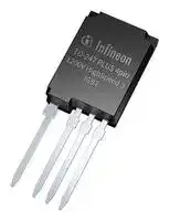
- Transistor Case Style: TO-247
- Operating Temperature Max: 175°C
- Continuous Collector Current: 150A
- Collector Emitter Voltage Max: 1.2kV
- Collector Emitter Saturation Voltage: 2V
| Delivery and price | |
|---|---|
| Units per pack | 250 |
| Price | 6.76 € |
| Current stock | 200+ |
| Lead time | 30 days |
IKY75N120CH3

## **Features:**

vj=175°C

CE(sat) Q G

http://www.infineon.com/igbt/

## **Applications:**

|**Type**|**_V_CE**|**_I_C**|**_V_CEsat** **_T_vj=25°C**|**_T_vjmax**|**Marking**|**Package**|
|---|---|---|---|---|---|---|
|IKY75N120CH3|1200V|75A|2V|175°C|K75MCH3|PG-TO247-4-2|


Datasheet www.infineon.com

2017-06-09

IKY75N120CH3

**==> picture [86 x 38] intentionally omitted <==**

## High�speed�switching�series�third�generation�IGBT

## **Table�of�Contents**

Description   . . . . . . . . . . . . . . . . . . . . . . . . . . . . . . . . . . . . . . . . . . . . . . . . . . . . . . . . . . . . . . . . . . . . . . . . 1 Table of Contents   . . . . . . . . . . . . . . . . . . . . . . . . . . . . . . . . . . . . . . . . . . . . . . . . . . . . . . . . . . . . . . . . . . . 2 Maximum Ratings  . . . . . . . . . . . . . . . . . . . . . . . . . . . . . . . . . . . . . . . . . . . . . . . . . . . . . . . . . . . . . . . . . . . 3 Thermal Resistance   . . . . . . . . . . . . . . . . . . . . . . . . . . . . . . . . . . . . . . . . . . . . . . . . . . . . . . . . . . . . . . . . . 3 Electrical Characteristics  . . . . . . . . . . . . . . . . . . . . . . . . . . . . . . . . . . . . . . . . . . . . . . . . . . . . . . . . . . . . . . 4 Electrical Characteristics Diagrams   . . . . . . . . . . . . . . . . . . . . . . . . . . . . . . . . . . . . . . . . . . . . . . . . . . . . . 6 Package Drawing   . . . . . . . . . . . . . . . . . . . . . . . . . . . . . . . . . . . . . . . . . . . . . . . . . . . . . . . . . . . . . . . . . . .13 Testing Conditions   . . . . . . . . . . . . . . . . . . . . . . . . . . . . . . . . . . . . . . . . . . . . . . . . . . . . . . . . . . . . . . . . . .14 Revision History   . . . . . . . . . . . . . . . . . . . . . . . . . . . . . . . . . . . . . . . . . . . . . . . . . . . . . . . . . . . . . . . . . . . .15 Disclaimer  . . . . . . . . . . . . . . . . . . . . . . . . . . . . . . . . . . . . . . . . . . . . . . . . . . . . . . . . . . . . . . . . . . . . . . . . .16

2

V�2.2 2017-06-09

Datasheet

IKY75N120CH3

**==> picture [86 x 38] intentionally omitted <==**

## High�speed�switching�series�third�generation�IGBT

## **Maximum�Ratings**

**For�optimum�lifetime�and�reliability,�Infineon�recommends�operating�conditions�that�do�not�exceed�80%�of�the�maximum�ratings�stated�in�this�datasheet.**

|**Parameter**|**Symbol**||**Value**|**Unit**|
|---|---|---|---|---|
|Collector-emittervoltage,_T_vj≥25°C|_V_CE||1200|V|
|DCcollectorcurrent,limitedby_T_vjmax<br>_T_C=25°C<br>_T_C=134°C|_I_C||150.0<br>75.0|A|
|Pulsedcollectorcurrent,_t_plimitedby_T_vjmax|_I_Cpuls||300.0|A|
|Turn off safe operating area<br>_V_CE≤1200V,_T_vj≤175°C,_t_p=1µs|-||300.0|A|
|Diodeforwardcurrent,limitedby_T_vjmax<br>_T_C=25°C<br>_T_C=100°C|_I_F||150.0<br>75.0|A|
|Diodepulsedcurrent,_t_plimitedby_T_vjmax|_I_Fpuls||300.0|A|
|Gate-emitter voltage<br>TransientGate-emittervoltage(_t_p≤10µs,_D_<0.010)|_V_GE||±20<br>±30|V|
|Short circuit withstand time<br>_V_GE=15.0V,_V_CC≤600V<br>Allowed number of short circuits < 1000<br>Time between short circuits:≥1.0s<br>_T_vj=175°C|_t_SC||10|µs|
|Powerdissipation_T_C=25°C<br>Powerdissipation_T_C=134°C|_P_tot||938.0<br>256.0|W|
|Operating junction temperature|_T_vj|-40...+175||°C|
|Storage temperature|_T_stg|-55...+150||°C|
|Soldering temperature,<br>wave soldering1.6mm(0.063in.)from case for 10s|||260|°C|


## **Thermal�Resistance**

|**ThermalResistance**|||||||
|---|---|---|---|---|---|---|
|**Parameter**|**Symbol **|**Conditions**||**Value**||**Unit**|
||||**min.**|**typ.**|**max.**||
|**RthCharacteristics**|||||||
|IGBT thermal resistance,1)<br>junction - case|_R_th(j-C)||-|-|0.16|K/W|
|Diode thermal resistance,1)<br>junction - case|_R_th(j-C)||-|-|0.28|K/W|
|Thermal resistance<br>junction - ambient|_R_th(j-a)||-|-|40|K/W|


1) Thermal resistance of thermal grease Rth(c-s) (case to heat sink) of more than 0.1K/W not included.

3

V�2.2 2017-06-09

Datasheet

IKY75N120CH3

**==> picture [86 x 38] intentionally omitted <==**

## High�speed�switching�series�third�generation�IGBT

## **Electrical�Characteristic,�at�** _**T**_ **vj�=�25°C,�unless�otherwise�specified**

|**Parameter**|**Symbol **|**Conditions**||**Value**||**Unit**|
|---|---|---|---|---|---|---|
||||**min.**|**typ.**|**max.**||
|**StaticCharacteristic**|||||||
|Collector-emitter breakdown voltage|_V_(BR)CES|_V_GE=0V,_I_C=0.50mA|1200|-|-|V|
|Collector-emitter saturation voltage|_V_CEsat|_V_GE=15.0V,_I_C=75.0A<br>_T_vj=25°C<br>_T_vj=175°C|-<br>-|2.00<br>2.50|2.35<br>-|V|
|Diode forward voltage|_V_F|_V_GE=0V,_I_F=75.0A<br>_T_vj=25°C<br>_T_vj=175°C|-<br>-|1.90<br>1.85|2.30<br>-|V|
|Gate-emitter threshold voltage|_V_GE(th)|_I_C=1.88mA,_V_CE=_V_GE|5.1|5.8|6.5|V|
|Zero gate voltage collector current|_I_CES|_V_CE=1200V,_V_GE=0V<br>_T_vj=25°C<br>_T_vj=175°C|-<br>-|-<br>5000|450<br>-|µA|
|Gate-emitter leakage current|_I_GES|_V_CE=0V,_V_GE=20V|-|-|100|nA|
|Transconductance|_g_fs|_V_CE=20V,_I_C=75.0A|-|26.0|-|S|


## **Electrical�Characteristic,�at�** _**T**_ **vj�=�25°C,�unless�otherwise�specified**

|**Parameter**|**Symbol **|**Conditions**||**Value**||**Unit**|
|---|---|---|---|---|---|---|
||||**min.**|**typ.**|**max.**||
|**DynamicCharacteristic**|||||||
|Input capacitance|_C_ies|_V_CE=25V,_V_GE=0V,f=1MHz|-|4856|-|pF|
|Output capacitance|_C_oes||-|505|-||
|Reverse transfer capacitance|_C_res||-|290|-||
|Gate charge|_Q_G|_V_CC=960V,_I_C=75.0A,<br>_V_GE=15V|-|370.0|-|nC|
|Internal emitter inductance<br>measured 5mm (0.197 in.) from<br>case|_L_E||-|13.0|-|nH|


## **Switching�Characteristic,�Inductive�Load**

|**Parameter**|**Symbol **|**Conditions**||**Value**||**Unit**|
|---|---|---|---|---|---|---|
||||**min.**|**typ.**|**max.**||
|**IGBTCharacteristic,at****_T_vj=25°C**|||||||
|Turn-on delaytime|_t_d(on)|_T_vj=25°C,<br>_V_CC=600V,_I_C=75.0A,<br>_V_GE=0.0/15.0V,<br>_R_G(on)=6.0Ω,_R_G(off)=6.0Ω,<br>_L_σ=70nH,_C_σ=67pF<br>_L_σ,_C_σfromFig.E<br>Energy losses include “tail” and<br>diode reverse recovery.|-|38|-|ns|
|Rise time|_t_r||-|32|-|ns|
|Turn-off delaytime|_t_d(off)||-|303|-|ns|
|Fall time|_t_f||-|32|-|ns|
|Turn-on energy|_E_on||-|3.40|-|mJ|
|Turn-off energy|_E_off||-|2.90|-|mJ|
|Total switchingenergy|_E_ts||-|6.30|-|mJ|


V�2.2 2017-06-09

Datasheet

4

IKY75N120CH3

**==> picture [86 x 38] intentionally omitted <==**

## High�speed�switching�series�third�generation�IGBT

**Diode�Characteristic,�at�** _**T**_ **vj�=�25°C**

|**DiodeCharacteristic,at****_T_vj=25°C**|||||||
|---|---|---|---|---|---|---|
|Diode reverse recoverytime|_t_rr|_T_vj=25°C,<br>_V_R=600V,<br>_I_F=75.0A,<br>_di_F_/dt_=1200A/µs|-|292|-|ns|
|Diode reverse recoverycharge|_Q_rr||-|4.90|-|µC|
|Diodepeak reverse recoverycurrent|_I_rrm||-|41.0|-|A|
|Diode peak rate of fall of reverse<br>recoverycurrentduring_t_b|_di_rr_/dt_||-|-585|-|A/µs|


## **Switching�Characteristic,�Inductive�Load**

|**Parameter**|**Symbol **|**Conditions**||**Value**||**Unit**|
|---|---|---|---|---|---|---|
||||**min.**|**typ.**|**max.**||
|**IGBTCharacteristic,at****_T_vj=175°C**|||||||
|Turn-on delaytime|_t_d(on)|_T_vj=175°C,<br>_V_CC=600V,_I_C=75.0A,<br>_V_GE=0.0/15.0V,<br>_R_G(on)=6.0Ω,_R_G(off)=6.0Ω,<br>_L_σ=70nH,_C_σ=67pF<br>_L_σ,_C_σfromFig.E<br>Energy losses include “tail” and<br>diode reverse recovery.|-|38|-|ns|
|Rise time|_t_r||-|35|-|ns|
|Turn-off delaytime|_t_d(off)||-|400|-|ns|
|Fall time|_t_f||-|68|-|ns|
|Turn-on energy|_E_on||-|6.10|-|mJ|
|Turn-off energy|_E_off||-|6.00|-|mJ|
|Total switchingenergy|_E_ts||-|12.10|-|mJ|


**Diode�Characteristic,�at�** _**T**_ **vj�=�175°C**

|Diode reverse recoverytime|_t_rr|_T_vj=175°C,<br>_V_R=600V,<br>_I_F=75.0A,<br>_di_F_/dt_=1200A/µs|-|538|-|ns|
|---|---|---|---|---|---|---|
|Diode reverse recoverycharge|_Q_rr||-|13.80|-|µC|
|Diodepeak reverse recoverycurrent|_I_rrm||-|60.0|-|A|
|Diode peak rate of fall of reverse<br>recoverycurrentduring_t_b|_di_rr_/dt_||-|-360|-|A/µs|


V�2.2 2017-06-09

Datasheet

5

IKY75N120CH3

**==> picture [474 x 313] intentionally omitted <==**

**----- Start of picture text -----**<br>
1000<br>ee<br>mT 900<br>100<br>tN 800<br>not for linear use<br>6= tm co me c iie}e 700 LAL| |<br>eB PN<br>600<br>10<br>A<br>500<br>5 400<br>2 FRESE eg | | | KA<br>A) BN<br>300<br>1<br>STE<br>& 200 FN<br>Ce CTC 100 \<br>0.1 0<br>TAM TMI EE | | | UN<br>1 10 100 1000 25 50 75 100 125 150 175<br>V CE , COLLECTOR-EMITTER VOLTAGE [V] T C , CASE TEMPERATURE [°C]<br>Figure 1. Forward bias safe operating area Figure 2. Power dissipation as a function of case<br>( D =0, T C =25°C, T vj 175°C; V GE=15V) temperature<br>I C P tot<br>**----- End of picture text -----**<br>


> Figure 2. Power **temperature** ( _T_ vj ≤ 175°C)

**==> picture [469 x 322] intentionally omitted <==**

**----- Start of picture text -----**<br>
160 300<br>VGE=20V<br>140 ST) FRE 17V<br>S 250 15V NZ<br>120 13V<br>ft  o N N/a<br>11V<br>200<br>oP NE ESS<br>100 9V<br>7V<br>80 150<br>ef NE EAR 5V<br>60<br>100<br>pp oa EA<br>40<br>50<br>HOEY PORES<br>20<br>ee ayZee<br>0 0<br>25 50 75 100 125 150 175 e e 0 1 Ae 2 3 4 5 6<br>T C , CASE TEMPERATURE [°C] V CE , COLLECTOR-EMITTER VOLTAGE [V]<br>Figure 3. Collector current as a function of case Figure 4. Typical output characteristic<br>temperature ( T vj=25°C)<br>( V GE ≥ 15V, T vj ≤ 175°C)<br>I C I C<br>**----- End of picture text -----**<br>


6

Datasheet

2017-06-09

IKY75N120CH3

**==> picture [471 x 313] intentionally omitted <==**

**----- Start of picture text -----**<br>
300 300<br>VGE=20V Tvj = 25°C<br>Ae LY Tvj = 175°C<br>17V<br>250 15V NN 250 e | |e |__!<br>_— ee e<br>13V<br>_ KNW ZA F e<br>11V<br>200 200<br>WW: 9V ROLL eeWW<br>a)NN 7V ae a) ee ee<br>150 150<br>e) 5V 4 e)<br>: ENN 2a Sf<br>: ENG CAs SE tt ep<br>100 100<br>: ) NW< ff ttat<br>| An<br>50 50<br>aeZc OG ee ee| | | | eee<br>AeZAI| | ON KO E ,<br>0 0<br>A g eee ee e e<br>0 1 2 3 4 5 6 2 4 6 8 10 12 14 16 18<br>V CE , COLLECTOR-EMITTER VOLTAGE [V] V GE , GATE-EMITTER VOLTAGE [V]<br>Figure 5. Typical output characteristic Figure 6. Typical transfer characteristic<br>( T vj=175°C) ( V CE=20V)<br>I C I C<br>**----- End of picture text -----**<br>


**==> picture [474 x 286] intentionally omitted <==**

**----- Start of picture text -----**<br>
4.5 1000<br>IC = 38A aa<br>IC = 75A aa ee ee<br>_ 4.0 = IC = 150A | - rr ee<br>= cle peers td(off) OO eee<br>tf<br>3.5 td(on)<br>tr<br>5 veo ry<br>100<br>pf oer e y<br>a 3.0 vo uw ——<br>o “7 = a ee eee<br>2.5<br>E | Q ee ee ee<br>2.0<br>Ww - 10 eT<br>1.5<br>° a ee<br>1.0<br>re a ee ee ee<br>0.5 1<br>25 50 75 100 125 150 175 0 30 60 90 120 150<br>T vj , JUNCTION TEMPERATURE [°C] I C , COLLECTOR CURRENT [A]<br>t<br>CEsat<br>V<br>**----- End of picture text -----**<br>


Figure 7. Typical a function ( _V_ GE=15V)

Figure 8.

**==> picture [88 x 9] intentionally omitted <==**

**----- Start of picture text -----**<br>
T vj =175°C, V CE=600V,<br>**----- End of picture text -----**<br>


_V_ GE =0/15V, _R_ G=6 Ω Figure E)

Datasheet

7

2017-06-09

IKY75N120CH3

**==> picture [230 x 274] intentionally omitted <==**

**----- Start of picture text -----**<br>
td(off)<br>tf<br>1000 td(on)<br>| tr ee es ee ee ee<br>1 a ee<br>po e<br>aee ee a eeee ee ee<br>ow ~~ Es | | | |<br>B |v}|) | | |<br>ee<br>=<br>oO<br>Zz _|<br>100<br>5 Jr<br>E a a Le Pd<br>a a a ae ae ee es<br>~ a a ee<br>10<br>0 5 10 15 20 25 30 35 40<br>R G , GATE RESISTOR [ Ω ]<br>t<br>**----- End of picture text -----**<br>


**==> picture [189 x 47] intentionally omitted <==**

**----- Start of picture text -----**<br>
Figure 9. Typical switching times as a<br>resistor<br>(inductive load, T vj =175°C, V CE=600V,<br>V GE =0/15V, I C =75A, Dynamic test<br>Figure E)<br>**----- End of picture text -----**<br>


**==> picture [233 x 329] intentionally omitted <==**

**----- Start of picture text -----**<br>
td(off)<br>tf<br>1000 td(on)<br>| tr a ee ee ee<br>1 a a a<br>a<br>ee eeee ee<br>- ~- | | | |<br>& | [pr]<br>=<br>oO<br>2<br>100<br>5 a es<br>a<br>a eeee<br>- po ee<br>10<br>25 50 75 100 125 150 175<br>T vj , JUNCTION TEMPERATURE [°C]<br>Figure 10. Typical switching times as a function of<br>junction temperature<br>(inductive load, V CE =600V, V GE=0/15V,<br>I C =75A, R G=6 , Dynamic test circuit in<br>Figure E)<br>t<br>**----- End of picture text -----**<br>


**==> picture [474 x 286] intentionally omitted <==**

**----- Start of picture text -----**<br>
8 35<br>typ. Eoff<br>min. Eon<br>max. Ets<br>7 30<br>uw /<br>x4 = /<br>F ~ /<br>fe) 6 — >>~ n£ 25 f/<br>Qa ~~. ~~ — 75) /<br>O > ~ ~sA ~ o /<br>5 5 — ~ ys = 20 /<br>Lu = ~~ yAL O 7<br>£ ~ ~ _ iT / /<br>e 4 oo |S~~ a 15 é /<br>La= — Zz . 7<br>i = “ y,<br>NN) E Vac Z Z|<br>3 10<br>O<br>~Y<br>2 5<br>a<br>1 0<br>25 50 75 100 125 150 175 0 30 60 90 120 150<br>T vj , JUNCTION TEMPERATURE [°C] I C , COLLECTOR CURRENT [A]<br>E<br>GE(th)<br>V<br>**----- End of picture text -----**<br>


Figure 11. of ( _I_ C=1mA)

Figure 12.

(inductive load, _T_ vj =175°C, _V_ CE=600V, _V_ GE =0/15V, _R_ G=6 Ω , Dynamic test Figure E)

8

Datasheet

2017-06-09

IKY75N120CH3

**==> picture [403 x 286] intentionally omitted <==**

**----- Start of picture text -----**<br>
30 14<br>Eoff Eoffoff<br>Eon Eonon<br>Ets Etsts<br>12<br>25 7<br>5 a 5<br>£& Y £&<br>op) vy (dp) 10<br>Lu 7 Lu a<br>7) 20 a 7) “<br>aa ;Y) vy Za ar a<br>ro) a 7 & 8 o<br>owy 15 vo vo 7 owyy pa . rae<br>6<br>© a oO ©<br>10<br>4<br>: Bee<br>3 L 3 b=<br>5<br>2<br>0 0<br>0 5 10 15 20 25 30 35 40 25 50 75 100<br>R G , GATE RESISTOR [ Ω ] T vj , JUNCTION<br>E E<br>**----- End of picture text -----**<br>


**==> picture [233 x 286] intentionally omitted <==**

**----- Start of picture text -----**<br>
14<br>Eoffoff<br>Eonon<br>Etsts<br>12<br>UA<br>5 <<br>£& a<br>(dp) 10 Pa<br>Lu a<br>7) “<br>ar a<br>& 8 o<br>owyy pa . rae<br>6<br>© — 1<br>4<br>3 b=<br>2<br>0<br>25 50 75 100 125 150 175<br>T vj , JUNCTION TEMPERATURE [°C]<br>E<br>**----- End of picture text -----**<br>


Figure 13.

Figure 14.

(inductive load, _V_ CE =600V, _V_ GE=0/15V, _I_ C =75A, _R_ G=6 , Dynamic test circuit in Figure E)

**==> picture [151 x 28] intentionally omitted <==**

**----- Start of picture text -----**<br>
(inductive load, T vj =175°C, V CE=600V,<br>V GE =0/15V, I C =75A, Dynamic test<br>Figure E)<br>**----- End of picture text -----**<br>


**==> picture [474 x 285] intentionally omitted <==**

**----- Start of picture text -----**<br>
18 16 P|<br>Eoff V CC<br>Eon 4“ — V CC  ==240v / yo<br>16 Ets 14 —-  =960V /<br>14<br>=) xO YY<br>12<br>wa oe Lu<br>LU Pa o<br>7) 12 x J<br>e) a 10<br>pa ae fe)<br>25 10 ’ ><br>or a a o 8<br>a 8 a ea E<br><= 2 am 6<br>ge) ee re<br>5 6 |__ Lot +7 | Ee<br>= | O<br>4<br>ea<br>4<br>2<br>2<br>0 0<br>400 450 500 550 600 650 700 750 800 0 50 100 150 200 250 300 350 400<br>V CE , COLLECTOR-EMITTER VOLTAGE [V] Q GE , GATE CHARGE [nC]<br>GE<br>V<br>E<br>**----- End of picture text -----**<br>


Figure 15.

Figure 16. Typical ( _I_ C=75A)

_T_ vj =175°C, _V_ GE=0/15V,

_I_ C =75A, _R_ G=6 Figure E)

9

Datasheet

2017-06-09

IKY75N120CH3

**==> picture [471 x 322] intentionally omitted <==**

**----- Start of picture text -----**<br>
600<br>Cies<br>Coes<br>1E+4 Cres<br>E S 500 A<br>El a——i)ee| ef Pree Ae<br>Se ee<br>400<br>SS ee ee<br>ro ee ee eee7<br>st2 | | | fe ELLExz | |<br>~¢ ul /<br>300<br>EF \\ a<br>O \ e) 4<br>2oO=< 1000 pAa1|S NTa Oe= {|Yt |<br>eee- a 2 A<br>Seee ee 200 r<br>a J.<br>a A<br>100<br>rest<br>EEETE Ty<br>100 0<br>0 5 10 15 20 25 30 10 11 12 13 14 15 16 17 18<br>V CE , COLLECTOR-EMITTER VOLTAGE [V] V GE , GATE-EMITTER VOLTAGE [V]<br>Figure 17. Typical capacitance as a function of Figure 18. Typical short circuit collector current as a<br>collector-emitter voltage function of gate-emitter voltage<br>( V GE =0V, f=1MHz) ( V CE 600V, T vj 175°C)<br>C<br>I C(SC)<br>**----- End of picture text -----**<br>


**==> picture [469 x 286] intentionally omitted <==**

**----- Start of picture text -----**<br>
45<br>D = 0.5<br>40 | > 0.1 0.2 pC Su mitt Se | ereee| il<br>_ = 0.1 NSECee<br>= Q 0.05<br>35<br>0.02<br>Ww Ww : 0 a a<br>= 9 0.01 ea<br>a < IN HME TNE TTL TT<br>30<br>2 o single pulse NDS<br>0.01<br>< | | 2 Fw ZUM<br>7p) Lu NIN LL ll y |<br>Ir 25 a PA et<br>- \ _Ix P IT ENNNUNN ATTTTe e neeiee<br>= S TC CNTIR NCAT TT<br>= Y MD 2921<br>E 20 | Wi or AM TAT<br>:S BENG F ELAMUTE ETA ELM Tl<br>15<br>n 0.001 LE EE ELL<br>~ ees 0 AA<br>Tr > s YT TT Ti —— Til<br>wn 10 a i | il<br>- SN - YN Cah IR, Co=te/Ro _||lI<br>~~ PTA TT TT oo<br>5 —_ Al ec<br>i: 1 2 3 4 5<br>ri[K/W]: 0.02275 0.047736 0.08788 2.0E-3 2.7E-4<br>τ i[s]: 3.8E-4 2.7E-3 0.019881 0.505051 12.95671<br>0 PEEL EEE ET 1E-4 A| |<br>10 12 14 16 18 20 1E-6 1E-5 1E-4 0.001 0.01 0.1 1<br>V GE , GATE-EMITTER VOLTAGE [V] t p , PULSE WIDTH [s]<br>t SC c)th(j-<br>Z<br>**----- End of picture text -----**<br>


Figure 19.

Figure 20. IGBT ( _D_ = _t_ p/T)

**==> picture [121 x 9] intentionally omitted <==**

**----- Start of picture text -----**<br>
( V CE 600V, start at T vj ≤ 175°C)<br>**----- End of picture text -----**<br>


10

Datasheet

2017-06-09

IKY75N120CH3

**==> picture [482 x 642] intentionally omitted <==**

**----- Start of picture text -----**<br>
1000<br>D = 0.5 Tvj = 25°C, IF = 75A<br>0.2 900 Tvj = 175°C, IF = 75A<br>0.1 0.1<br>x ‘ii AC) —| — K K<br>wo 0.05 FES CE eA 800 Lo]<br>9 FTA 0.02 CTI aT 2 = \<br>< 0.01 NN TP aT 700 \<br>single pulse<br>D STAT Tt 2 600 Poy ON<br>es 0.01 00 “<br>Zz EN NAS CES > ><br>feSESANC SILC8 500 ‘ ~ Nn<br>Rs: SePUTTIN AVA ETI PM LE aIN 400 NN ~<br>300<br>0.001<br>I/IIZ ry MCI) & | |<br>e AP a h an ee -——_<br>FE | RSHED) os | 200 ———<br>- PLANPANEI TL ci=Avrs Comrie Ill<br>i: 1 2 3 4 5 100<br>| E [[ene] TI ri[K/W]: 0.01104 PEIN 0.10889 ETT 0.1573 ETT 2.8E-3 3.0E-4 TTT Pf fff]<br>τ i[s]: 3.6E-4 2.7E-3 0.01681 0.44863 12.11241<br>1E-4 Al | 0 Pf of ft td<br>1E-6 1E-5 1E-4 0.001 0.01 0.1 1 400 600 800 1000 1200 1400 1600<br>t p , PULSE WIDTH [s] di F /dt , DIODE CURRENT SLOPE [A/us]<br>Figure 21. Diode transient thermal impedance as a Figure 22. Typical reverse recovery time as a function<br>function of pulse width of diode current slope<br>( D = t p/T) ( V R=600V)<br>18 90<br>Tvj = 25°C, IF = 75A Tvj = 25°C, IF = 75A<br>Tvj = 175°C, IF = 75A Tvj = 175°C, IF = 75A<br>Eo)<br>16 80<br>| Eo<br>14 70<br>gf fe |<br>ng ee ind ee7<br>+ 12 & 60 7<br>>ee(aaef 10 > 50 EeeYZ<br>8o 8 ©O 40 4 4ma<br>pg<br>2 6 2 30 a<br>2 ee eee<br>4 20<br>PEPE? 2 10 EEE<br>0 0<br>400 600 800 1000 1200 1400 1600 400 600 800 1000 1200 1400 1600<br>di F /dt , DIODE CURRENT SLOPE [A/us] di F /dt , DIODE CURRENT SLOPE [A/us]<br>t rr<br>c)th(j-<br>Z<br>Q rr I rr<br>**----- End of picture text -----**<br>


Figure 23. Typical function ( _V_ R=600V)

Figure 24.

( _V_ R=600V)

11

Datasheet

2017-06-09

IKY75N120CH3

**==> picture [473 x 285] intentionally omitted <==**

**----- Start of picture text -----**<br>
0 300<br>Tvj = 25°C, IF = 75A Tvj = 25°C<br>-100 Se Tvj = 175°C, IF e  = 75A e e See Tvj = 175°C<br>250 ff<br>z -200 Nee se<br>|7 — ~ P pAy<br>-300<br>* X N o e<br>vo ~~ 200<br>pS) INN<br>-400<br>5& N \ na /<br>eto |UKN 8 EE<br>ef& -500 ||X| aNE 150 LE<br>-600<br>100<br>ef | | iN fs Pez |<br>-700<br>ee ~ t] [TTY] TT] |<br>-800<br>50<br>-900 ee ee4a<br>-1000 0<br>ee e e eane<br>400 600 800 1000 1200 1400 1600 0.0 0.5 1.0 1.5 2.0 2.5 3.0 3.5 4.0 4.5<br>di F /dt , DIODE CURRENT SLOPE [A/us] V F , FORWARD VOLTAGE [V]<br>I rr<br>/dt I F<br>rr<br>dI<br>**----- End of picture text -----**<br>


Figure 25.

Figure 26.

( _V_ R=600V)

**==> picture [233 x 286] intentionally omitted <==**

**----- Start of picture text -----**<br>
3.5<br>IF = 38A<br>IF = 75A<br>IF = 150A<br>3.0<br>2.5<br>ke<br>I<br>e)<br>><br>QWw 2.0 Pi} | tl<br>aa<br><x<br>x<br>(e)<br>1.5<br>1.0<br>0.5<br>25 50 75 100 125 150 175<br>T vj , JUNCTION TEMPERATURE [°C]<br>F<br>V<br>**----- End of picture text -----**<br>


Figure 27.

12

Datasheet

2017-06-09

IKY75N120CH3

**==> picture [86 x 38] intentionally omitted <==**

## High�speed�switching�series�third�generation�IGBT

## **PG-TO247-4-2**

**==> picture [415 x 299] intentionally omitted <==**

**----- Start of picture text -----**<br>
M<br>A<br>E<br>A2 E2<br>R<br>b2<br>b4<br>E3 b6 H<br>2x<br>E1<br>1 2 3 4<br>b 4 3 2 1<br>e1 A1<br>e<br>b7<br>c<br>D3<br>D1 D D2<br>D4<br>N<br>L1<br>L<br>**----- End of picture text -----**<br>


**==> picture [84 x 32] intentionally omitted <==**

PACKAGE SURFACE ROUTE BETWEEN PIN 1 & PIN 2 WILL BE 5.1mm MIN.

**==> picture [185 x 271] intentionally omitted <==**

**----- Start of picture text -----**<br>
MILLIMETERS<br>DIMENSION<br>MIN. MAX.<br>A 4.9 5.1<br>A1 2.31 2.51<br>A2 1.9 2.1<br>b 1.16 1.29<br>b2 1.36 1.49<br>b4 2.16 2.29<br>b6 1.16 1.45<br>b7 1.16 1.65<br>c 0.59 0.66<br>D 20.9 21.1<br>D1 22.3 22.5<br>D2 15.95 16.55<br>D3 1 1.35<br>D4 1.6 1.8<br>E 15.7 15.9<br>E1 3.9 4.1<br>E2 13.1 13.5<br>E3 2.58 2.78<br>e 2.54<br>e1 5.08<br>H 0.8 1<br>L 19.8 20.1<br>L1 2.55 2.85<br>M 0.97 1.57<br>N 3.24 3.44<br>R 1.9 2.1<br>**----- End of picture text -----**<br>


ALL b... AND c DIMENSIONS INCLUDING PLATING EXCEPT AREA OF CUTTING

**==> picture [98 x 183] intentionally omitted <==**

**----- Start of picture text -----**<br>
DOCUMENT NO.<br>Z8B00182798<br>REVISION<br>01<br>SCALE 2:1<br>0 5 10mm<br>EUROPEAN PROJECTION<br>ISSUE DATE<br>23.09.2016<br>**----- End of picture text -----**<br>


13

V�2.2 2017-06-09

Datasheet

IKY75N120CH3

**==> picture [86 x 38] intentionally omitted <==**

## High�speed�switching�series�third�generation�IGBT

## **Testing Conditions**

**==> picture [252 x 588] intentionally omitted <==**

**----- Start of picture text -----**<br>
V GE (t)<br>90%  V GE<br>10%  V GE t<br>I C (t)<br>90%  I C 90%  I C<br>10%  I C 10%  I C<br>t<br>V CE (t)<br>t<br>t d(off) t f t d(on) t r<br>Figure A.<br>V GE (t)<br>90%  V GE<br>10%  V GE<br>t<br>I C (t)<br>2%  I C t<br>V CE (t)<br>t 2 t 4<br>E off  [=] V CE x I C x d t E on  [=] V CE x I C x d t<br>t 1 t 3 2%  V CE<br>t<br>t 1 t 2 t 3 t 4<br>Figure B.<br>**----- End of picture text -----**<br>


**==> picture [189 x 170] intentionally omitted <==**

**----- Start of picture text -----**<br>
I,V<br>dI F /dt Qt rrrr== Qt aa++ tQ b b<br>a b<br>Q a Q b<br>dI<br>Figure C.  Definition of diode switching<br>characteristics<br>**----- End of picture text -----**<br>


**==> picture [7 x 7] intentionally omitted <==**

**----- Start of picture text -----**<br>
t<br>**----- End of picture text -----**<br>


**==> picture [169 x 63] intentionally omitted <==**

Figure D.

**==> picture [7 x 4] intentionally omitted <==**

**----- Start of picture text -----**<br>
CC<br>**----- End of picture text -----**<br>


Figure E. **Dynamic test circuit** Parasitic inductance Ls, parasitic capacitor Cs, relief capacitor C ,r (only for ZVT switching)

14

V�2.2 2017-06-09

Datasheet

IKY75N120CH3

**==> picture [86 x 38] intentionally omitted <==**

## High�speed�switching�series�third�generation�IGBT

## **Revision�History**

IKY75N120CH3

## **Revision:�2017-06-09,�Rev.�2.2**

## Previous Revision

|Revision|Date|Subjects(major changes since last revision)|
|---|---|---|
|2.1|2017-04-26|Final data sheet|
|2.2|2017-06-09|Update Figure 6|


15

V�2.2 2017-06-09

Datasheet

## party.

## **Warnings**
Updated at June 9, 2026
Infineon Technologies is a globally recognized leader in semiconductor solutions, renowned for driving innovation in power management, energy efficiency, and modern mobility. With a strong legacy of engineering excellence, the company provides highly reliable components designed to meet the rigorous demands of industrial, automotive, and advanced commercial applications. The core of our Infineon portfolio is centered on their industry-leading discrete semiconductors. We offer an extensive selection of single and dual MOSFETs, alongside a robust range of single IGBTs and advanced IGBT modules. These flagship power transistors are essential for high-efficiency power conversion and motor control, providing engineers with superior thermal performance and minimized switching losses. Beyond advanced field-effect transistors, the selection includes a comprehensive array of diodes and rectifiers, heavily featuring Schottky diodes, as well as fast-recovery and RF/PIN diodes. This power foundation is further supported by bipolar transistors, intelligent power modules, and thyristor SCR modules, delivering the critical building blocks required for complex power system designs. To support broader system integration, the portfolio also encompasses specialized solutions such as solid-state relays, AC/DC LED driver ICs, and Bluetooth communications modules. From high-power industrial rectifiers to wireless connectivity adapters, Infineon equips designers with the precision components needed to build efficient, scalable, and fully connected electronic systems.
About Novapart
Novapart is a B2B electronic component broker specialising in stock shortages and cost reduction. We source hard-to-find parts and identify compliant alternatives across a catalogue of 410,000+ components from 500+ manufacturers.
Learn more →Stock Shortage Specialist
When a component is unavailable, discontinued or has an unacceptable lead time, we tap into our network of vetted European and Asian distributors to source what you need — without compromising on quality or traceability.
Request a quote →Compliant Alternatives
We identify pin-to-pin, electrically equivalent substitutes that meet the same certifications (RoHS, AEC-Q100, REACH) as your original specification — validated against datasheets, not just part numbers. Often at a lower cost.
BOM Analysis service →