


IKD15N60RFATMA1
IGBT, 30 A, 2.2 V, 250 W, 600 V, TO-252 (DPAK), 3 Pins
- Manufacturer: INFINEON
- Product type: Single IGBTs
- DC Collector Current:30A; Collector Emitter Saturation Voltage Vce(on):2.2V; Power Dissipation Pd:250W; Collector Emitter Voltage V(br)ceo:600V; Transistor Case Style:TO-252; No. of Pins:
- MSL: -
- SVHC: No SVHC (25-Jun-2025)
- No. of Pins: 3Pins
- Product Range: TRENCHSTOP RC
- Power Dissipation: 250W
- Transistor Mounting: Surface Mount
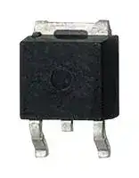
- Transistor Case Style: TO-252 (DPAK)
- Operating Temperature Max: 175°C
- Continuous Collector Current: 30A
- Collector Emitter Voltage Max: 600V
- Collector Emitter Saturation Voltage: 2.2V
| Delivery and price | |
|---|---|
| Units per pack | 5000 |
| Price | 0.532 € |
| Current stock | 1000+ |
| Lead time | 30 days |
## IGBT

IKD15N60RF TRENCHSTOP[TM]

## IKD15N60RF

## TRENCHSTOP[TM]

**==> picture [469 x 217] intentionally omitted <==**

**----- Start of picture text -----**<br>
Features: C<br>TRENCHSTOP [TM] Reverse Conducting (RC) technology for 600V<br>applications offering<br>¢ Optimized Eon, Eoff and Qrr for low switching losses<br>G<br>¢ Operating range of 4 to 30kHz<br>E<br>* Smooth switching performance leading to low EMI levels<br>¢ Very tight parameter distribution<br>* Maximum junction temperature 175°C<br>¢ Short circuit capability of 5us C<br>* Best in class current versus package size performance a<br>* Qualified according to JEDEC for target applications "6.73 Mean<br>¢ Pb-free lead plating; ROHS compliant (solder temperature er)<br>260°C, MSL1) x a /<br>G<br>Complete product spectrum and PSpice Models: ao<br>http://www.infineon.com/igbt/ E<br>Applications:<br>**----- End of picture text -----**<br>


|**Type**|**_V_CE**|**_I_C**|**_V_CEsat** **_T_vj=25°C**|**_T_vjmax**|**Marking**|**Package**|
|---|---|---|---|---|---|---|
|IKD15N60RF|600V|15A|2.2V|175°C|K15R60F|PG-TO252-3|


2

IKD15N60RF

**==> picture [146 x 65] intentionally omitted <==**

## TRENCHSTOP[TM] �RC-Drives�Fast�Series

## **Table�of�Contents**

Description   . . . . . . . . . . . . . . . . . . . . . . . . . . . . . . . . . . . . . . . . . . . . . . . . . . . . . . . . . . . . . . . . . . . . . . . . 2 Table of Contents   . . . . . . . . . . . . . . . . . . . . . . . . . . . . . . . . . . . . . . . . . . . . . . . . . . . . . . . . . . . . . . . . . . . 3 Maximum ratings  . . . . . . . . . . . . . . . . . . . . . . . . . . . . . . . . . . . . . . . . . . . . . . . . . . . . . . . . . . . . . . . . . . . . 4 Thermal Resistance   . . . . . . . . . . . . . . . . . . . . . . . . . . . . . . . . . . . . . . . . . . . . . . . . . . . . . . . . . . . . . . . . . 4 Electrical Characteristics  . . . . . . . . . . . . . . . . . . . . . . . . . . . . . . . . . . . . . . . . . . . . . . . . . . . . . . . . . . . . . . 5 Electrical Characteristics diagrams  . . . . . . . . . . . . . . . . . . . . . . . . . . . . . . . . . . . . . . . . . . . . . . . . . . . . . . 8 Package Drawing   . . . . . . . . . . . . . . . . . . . . . . . . . . . . . . . . . . . . . . . . . . . . . . . . . . . . . . . . . . . . . . . . . . .15 Testing Conditions   . . . . . . . . . . . . . . . . . . . . . . . . . . . . . . . . . . . . . . . . . . . . . . . . . . . . . . . . . . . . . . . . . .16 Revision History   . . . . . . . . . . . . . . . . . . . . . . . . . . . . . . . . . . . . . . . . . . . . . . . . . . . . . . . . . . . . . . . . . . . .17 Disclaimer  . . . . . . . . . . . . . . . . . . . . . . . . . . . . . . . . . . . . . . . . . . . . . . . . . . . . . . . . . . . . . . . . . . . . . . . . .17

3

Rev.�2.3,��2014-03-12

IKD15N60RF

**==> picture [146 x 65] intentionally omitted <==**

## TRENCHSTOP[TM] �RC-Drives�Fast�Series

## **Maximum�ratings**

|**Maximumratings**|||||
|---|---|---|---|---|
|**Parameter**|**Symbol**||**Value**|**Unit**|
|Collector-emittervoltage,_T_vj≥25°C|_V_CE||600|V|
|DCcollectorcurrent,limitedby_T_vjmax<br>_T_C=25°C<br>_T_C=100°C|_I_C||30.0<br>15.0|A|
|Pulsedcollectorcurrent,_t_plimitedby_T_vjmax|_I_Cpuls||45.0|A|
|Turn off safe operating area<br>_V_CE≤600V,_T_vj≤175°C,_t_p=1µs|-||35.0|A|
|Diodeforwardcurrent,limitedby_T_vjmax<br>_T_C=25°C<br>_T_C=100°C|_I_F||30.0<br>15.0|A|
|Diodepulsedcurrent,_t_plimitedby_T_vjmax|_I_Fpuls||45.0|A|
|Gate-emitter voltage|_V_GE||±20|V|
|Short circuit withstand time<br>_V_GE=15.0V,_V_CC≤400V<br>Allowed number of short circuits < 1000<br>Time between short circuits:≥1.0s<br>_T_vj=150°C|_t_SC||5|µs|
|Powerdissipation_T_C=25°C|_P_tot||250.0|W|
|Operating junction temperature|_T_vj|-40...+175||°C|
|Storage temperature|_T_stg|-55...+150||°C|
|Soldering temperature,<br>reflow soldering (MSL1 accordingto JEDEC J-STA-020)|||260|°C|


## **Thermal�Resistance**

|**ThermalResistance**||||||
|---|---|---|---|---|---|
|**Parameter**|**Symbol **|**Conditions**|**Max.Value**||**Unit**|
|**Characteristic**||||||
|IGBT thermal resistance,1)<br>junction - case|_R_th(j-c)|||0.60|K/W|
|Diode thermal resistance,2)<br>junction - case|_R_th(j-c)|||2.00|K/W|
|Thermal resistance, min. footprint<br>junction - ambient|_R_th(j-a)|||75|K/W|
|Thermal resistance, 6cm² Cu on<br>PCB<br>junction - ambient|_R_th(j-a)|||50|K/W|


1) Rth/Zth based on single cooling pulse. Please be aware that a correct Rth measurement of the IGBT, is not possible using a thermocouple.

2) Rth/Zth based on single cooling pulse. Please be aware that a correct Rth measurement of the Diode, is not possible using a thermocouple.

Rev.�2.3,��2014-03-12

4

IKD15N60RF

TRENCHSTOP[TM] �RC-Drives�Fast�Series

**==> picture [146 x 65] intentionally omitted <==**

## **Electrical�Characteristic,�at�** _**T**_ **vj�=�25°C,�unless�otherwise�specified**

|**Parameter**|**Symbol **|**Conditions**||**Value**||**Unit**|
|---|---|---|---|---|---|---|
||||**min.**|**typ.**|**max.**||
|**StaticCharacteristic**|||||||
|Collector-emitter breakdown voltage|_V_(BR)CES|_V_GE=0V,_I_C=0.20mA|600|-|-|V|
|Collector-emitter saturation voltage|_V_CEsat|_V_GE=15.0V,_I_C=15.0A<br>_T_vj=25°C<br>_T_vj=175°C|-<br>-|2.20<br>2.30|2.50<br>-|V|
|Diode forward voltage|_V_F|_V_GE=0V,_I_F=15.0A<br>_T_vj=25°C<br>_T_vj=175°C|-<br>-|2.10<br>2.00|2.40<br>-|V|
|Gate-emitter threshold voltage|_V_GE(th)|_I_C=0.25mA,_V_CE=_V_GE|4.3|5.0|5.7|V|
|Zero gate voltage collector current1)|_I_CES|_V_CE=600V,_V_GE=0V<br>_T_vj=25°C<br>_T_vj=175°C|-<br>-|-<br>-|40.0<br>1000.0|µA|
|Gate-emitter leakage current|_I_GES|_V_CE=0V,_V_GE=20V|-|-|100|nA|
|Transconductance|_g_fs|_V_CE=20V,_I_C=15.0A|-|6.6|-|S|
|Integratedgate resistor|_r_G|||none||Ω|


## **Electrical�Characteristic,�at�** _**T**_ **vj�=�25°C,�unless�otherwise�specified**

|**Parameter**|**Symbol **|**Conditions**||**Value**||**Unit**|
|---|---|---|---|---|---|---|
||||**min.**|**typ.**|**max.**||
|**DynamicCharacteristic**|||||||
|Input capacitance|_C_ies|_V_CE=25V,_V_GE=0V,f=1MHz|-|961|-|pF|
|Output capacitance|_C_oes||-|53|-||
|Reverse transfer capacitance|_C_res||-|33|-||
|Gate charge|_Q_G|_V_CC=480V,_I_C=15.0A,<br>_V_GE=15V|-|90.0|-|nC|
|Internal emitter inductance<br>measured 5mm (0.197 in.) from<br>case|_L_E||-|7.0|-|nH|
|Short circuit collector current<br>Max. 1000 short circuits<br>Time between short circuits:≥1.0s|_I_C(SC)|_V_GE=15.0V,_V_CC≤400V,<br>_t_SC≤5µs<br>_T_vj=25°C|-|112|-|A|


1) Not subject to production test - verified by design/characterization

Rev.�2.3,��2014-03-12

5

IKD15N60RF

TRENCHSTOP[TM] �RC-Drives�Fast�Series

**==> picture [146 x 65] intentionally omitted <==**

## **Switching�Characteristic,�Inductive�Load**

|**Parameter**|**Symbol **|**Conditions**||**Value**||**Unit**|
|---|---|---|---|---|---|---|
||||**min.**|**typ.**|**max.**||
|**IGBTCharacteristic,at****_T_vj=25°C**|||||||
|Turn-on delaytime|_t_d(on)|_T_vj=25°C,<br>_V_CC=400V,_I_C=15.0A,<br>_V_GE=0.0/15.0V,<br>_r_G=15.0Ω,_L_σ=50nH,<br>_C_σ=34pF<br>_L_σ,_C_σfromFig.E|-|13|-|ns|
|Rise time|_t_r||-|15|-|ns|
|Turn-off delaytime|_t_d(off)||-|160|-|ns|
|Fall time|_t_f||-|17|-|ns|
|Turn-on energy|_E_on||-|0.27|-|mJ|
|Turn-off energy|_E_off||-|0.25|-|mJ|
|Total switchingenergy|_E_ts||-|0.52|-|mJ|


**Diode�Characteristic,�at�** _**T**_ **vj�=�25°C**

|Diode reverse recoverytime|_t_rr|_T_vj=25°C,<br>_V_R=400V,<br>_I_F=15.0A,<br>_di_F_/dt_=1030A/µs|-|74|-|ns|
|---|---|---|---|---|---|---|
|Diode reverse recoverycharge|_Q_rr||-|0.42|-|µC|
|Diodepeak reverse recoverycurrent|_I_rrm||-|13.2|-|A|
|Diode peak rate of fall of reverse<br>recoverycurrentduring_t_b|_di_rr_/dt_||-|-211|-|A/µs|


## **Switching�Characteristic,�Inductive�Load**

|**Parameter**|**Symbol **|**Conditions**||**Value**||**Unit**|
|---|---|---|---|---|---|---|
||||**min.**|**typ.**|**max.**||
|**IGBTCharacteristic,at****_T_vj=175°C**|||||||
|Turn-on delaytime|_t_d(on)|_T_vj=175°C,<br>_V_CC=400V,_I_C=15.0A,<br>_V_GE=0.0/15.0V,<br>_r_G=15.0Ω,_L_σ=50nH,<br>_C_σ=34pF<br>_L_σ,_C_σfromFig.E|-|13|-|ns|
|Rise time|_t_r||-|17|-|ns|
|Turn-off delaytime|_t_d(off)||-|173|-|ns|
|Fall time|_t_f||-|20|-|ns|
|Turn-on energy|_E_on||-|0.45|-|mJ|
|Turn-off energy|_E_off||-|0.33|-|mJ|
|Total switchingenergy|_E_ts||-|0.78|-|mJ|


**Diode�Characteristic,�at�** _**T**_ **vj�=�175°C**

|Diode reverse recoverytime|_t_rr|_T_vj=175°C,<br>_V_R=400V,<br>_I_F=15.0A,<br>_di_F_/dt_=880A/µs|-|142|-|ns|
|---|---|---|---|---|---|---|
|Diode reverse recoverycharge|_Q_rr||-|1.00|-|µC|
|Diodepeak reverse recoverycurrent|_I_rrm||-|16.6|-|A|
|Diode peak rate of fall of reverse<br>recoverycurrentduring_t_b|_di_rr_/dt_||-|-133|-|A/µs|


6

Rev.�2.3,��2014-03-12

RC-Drives Fast Series IKD15N60RF

TRENCHSTOP[TM]

**==> picture [476 x 341] intentionally omitted <==**

**----- Start of picture text -----**<br>
10<br>9<br>- PL VII OA DI<br>7A | AT<br>8<br>CPST 10 OSS<br><x 7 ’ < oeny<br>= oe<br>Zz : i i i = Ee eee A cee ee Sl<br>6 a Zz PT | tp I =10µs Ae Cet PUTT<br>6<br>cpm LAM LM @ | eer<br>20µs<br>ST MT 8 Goes<br>C 5 ee ee aeeel<br>BL 4 UIETAIT 100µs50µs<br>2 UTI| 2 1 |[ptm |rue!<br>= = ee ee eel<br>200µs<br>SUE 3 \ 5) ee<br>5) UWI UI) ¢ SSee<br>500µs<br>- - OLEH<br>2 DC<br>OU TANMLUIEIN °F ead<br>1 CCCI EEC<br>oi<br>0 0.1<br>0.1 1 10 100 1 10 100 1000<br>f , SWITCHING FREQUENCY [kHz] V CE , COLLECTOR-EMITTER VOLTAGE [V]<br>Figure 1. Collector current as a function of switching Figure 2. Forward bias safe operating area<br>frequency ( D =0, T C =25°C, T vj 175°C; V GE=15V)<br>( T vj ≤ 175°C, T a =55°C, D =0.5, V CE=400V,<br>V GE =15/0V, r G=15 Ω , PCB mounting with<br>thermal vias and heatsink, see Appnote:<br>www.infineon.com/igbt)<br>I C I C<br>**----- End of picture text -----**<br>


**==> picture [233 x 275] intentionally omitted <==**

**----- Start of picture text -----**<br>
250<br>225<br>200<br>p\ | | ff<br>175<br>esz= {| \)|)<br>6= 150 fo v6\ Ud]<br>o<br>é<br>p | IN |<br>125<br>3<br>ef | AX<br>WW 100<br>&<br>P| |TN<br>75<br>BI<br>50<br>25<br>0<br>25 50 75 100 125 150 175<br>T C , CASE TEMPERATURE [°C]<br>tot<br>P<br>**----- End of picture text -----**<br>


> Figure 3. Power **temperature** ( _T_ vj ≤ 175°C)

**==> picture [233 x 256] intentionally omitted <==**

**----- Start of picture text -----**<br>
30<br>N ee<br>25<br>|e POX<br>E<br>or 20 EN<br>a)<br>Ss ft | AT | ft<br>fs<br>e 15 | | | tN | ft<br>8<br>im<br>ge ft | | | Af ft<br>tg 10 FN<br> BAN<br>5<br>0<br>0 25 50 75 100 125 150 175<br>T C , CASE TEMPERATURE [°C]<br>I C<br>**----- End of picture text -----**<br>


Figure 4. Collector current as **temperature** ( _V_ GE ≥ 15V, _T_ vj ≤ 175°C)

7

## TRENCHSTOP[TM]

## RC-Drives Fast Series

## IKD15N60RF

**==> picture [469 x 302] intentionally omitted <==**

**----- Start of picture text -----**<br>
45 45<br>VGE=20V<br>40 40<br>pos 17V EE<br>mS<br>35 15V 35 VGE=20V<br>13V 17V<br>: 30 V/A 30 SW<br>11V 15V<br>25 9V 25 13V<br>7V 11V<br>PSS) 20  oS 20<br>9V<br>BERG 0/48 genes 22<br>7V<br>15 15<br>S) S) L<br>10 10<br>5 5<br>JN<br>| LAR<br>A<br>0 0<br>O L Lae<br>0 1 2 3 4 0 1 2 3 4<br>V CE , COLLECTOR-EMITTER VOLTAGE [V] V CE , COLLECTOR-EMITTER VOLTAGE [V]<br>Figure 5. Typical output characteristic Figure 6. Typical output characteristic<br>( T vj=25°C) ( T vj=175°C)<br>I C I C<br>**----- End of picture text -----**<br>


**==> picture [474 x 276] intentionally omitted <==**

**----- Start of picture text -----**<br>
45 4.0<br>Tj=25°C IC=1A<br>a Tj=175°C IC=5A<br>40 3.5 IC=15A<br>IC=30A<br>i i i ee ae<br>35<br>alle F ee<br>, Ee 3.0<br>_ y |<br>30<br>eee P r<br>2.5<br>Bf ye<br>nee 25 eee 2.0<br>20<br>1.5<br>ee eee:: Bf fefecatefenten<br>15<br>: ; et<br>1.0<br>10<br>L TLL LLL ===<br>ppb ye 0.5 fan<br>5<br>0 0.0<br>L ALZT.  TEL Bae<br>4 6 8 10 12 14 0 25 50 75 100 125 150 175<br>V GE , GATE-EMITTER VOLTAGE [V] T vj , JUNCTION TEMPERATURE [°C]<br>I C<br>CEsat<br>V<br>**----- End of picture text -----**<br>


Figure 7. Typical ( _V_ CE=10V)

Figure 8.

( _V_ GE=15V)

8

RC-Drives Fast Series IKD15N60RF

## TRENCHSTOP[TM]

**==> picture [471 x 331] intentionally omitted <==**

**----- Start of picture text -----**<br>
1000<br>td(off)<br>| | | | dT dT | tf _ a A tf SS ES ES ES ES<br>se I td(on) ee<br>tr<br>100<br>e 1 s td(off) aee ee ee| | yt |I [ | a= [ber]] [|ee| |<br>tf<br>n td(on) n<br>e fe tr ee 100 L ee<br>ee a ee<br>= | [Crtpeebeefe-tede]<br>9 _a tc Pe] 2Q e pee e ee eeeeee<br>i 10 a a ee ee i — wed<br>10<br>( PES EEE § GEESE LL<br>Ne NS ———_———<br>ee eee a a<br>Pet f ft ct a<br>pf} | ft tt | Pot | | | cE ET<br>1 1<br>7.5 10.0 12.5 15.0 17.5 20.0 22.5 25.0 27.5 30.0 5 10 15 20 25 30 35 40 45 50<br>I C , COLLECTOR CURRENT [A] r G , GATE RESISTOR [ Ω ]<br>Figure 9. Typical switching times as a function of Figure 10. Typical switching times as a function of<br>collector current resistor<br>(inductive load, T vj =175°C, V CE=400V, (inductive load, T vj =175°C, V CE=400V,<br>V GE =15/0V, r G=15 Ω , Dynamic test circuit in V GE =15/0V, I C =15A, Dynamic test circuit in<br>Figure E) Figure E)<br>t t<br>**----- End of picture text -----**<br>


**==> picture [489 x 276] intentionally omitted <==**

**----- Start of picture text -----**<br>
7<br>td(off) typ.<br>tf min.<br>td(on) max.<br>tr 6<br>ee ee ee2<br>e)<br>< Q 5<br>o 100<br>Ww a 5 ee<br>=F a eeee 7)<br>a ee ee<br>4<br>9 ee eee me _<br>a ee ee ee x —_ a<br>rm a<br>3<br>2<br>10 1<br>25 50 75 100 125 150 175 25 50 75 100 125 150 175<br>T vj , JUNCTION TEMPERATURE [°C] T vj , JUNCTION TEMPERATURE [°C]<br>t<br>GE(th)<br>V<br>**----- End of picture text -----**<br>


Figure 11.

**==> picture [91 x 9] intentionally omitted <==**

**----- Start of picture text -----**<br>
V CE =400V, V GE=15/0V,<br>**----- End of picture text -----**<br>


Figure 12.

( _I_ C=0,25mA)

_I_ C =15A, _r_ G=15 Figure E)

9

IKD15N60RF

## TRENCHSTOP[TM]

**==> picture [474 x 623] intentionally omitted <==**

**----- Start of picture text -----**<br>
2.0 1.4<br>Eoff Eoff<br>Eon Eon<br>Ets Ets<br>1.2<br>5 “le E |)>.| bet |<br>1.5<br>uw aa Ww 1.0<br>o2 a4 oBop<br>r rere 7 7 a9 | | | ke} |<br>—! —!<br>S | ee 0.8 ee<br>4 a Pe<br>Ww 1.0 ow aw cee<br>Zz . v7 s WWZz : “7 =<br>2 | “ oc (0) 0.6 L-7<br>I £ 2 fer<br>“ a = oe —.-<br>0.4<br>0.5<br>*5 7 a TeteTT | | tt<br>0.2<br>Seen[letee(eeeeTy | |S PTPree yy fy<br>0.0 0.0<br>7.5 10.0 12.5 15.0 17.5 20.0 22.5 25.0 27.5 30.0 5 10 15 20 25 30 35 40 45 50<br>I C , COLLECTOR CURRENT [A] r G , GATE RESISTOR [ Ω ]<br>Figure 13. Typical switching energy losses as a Figure 14. Typical switching energy losses as a<br>function of collector current function of gate resistor<br>(inductive load, T vj =175°C, V CE=400V, (inductive load, T vj =175°C, V CE=400V,<br>V GE =15/0V, r G=15 Ω , Dynamic test circuit in V GE =15/0V, I C =15A, Dynamic test circuit in<br>Figure E) Figure E)<br>0.9 1.0<br>Eoff Eoff<br>Eon Eon<br>0.8 F Ets L L...| PLL Ets<br>; ee 0.8<br>0.7<br>7) 7) ”<br>ep) ep)<br>0.6<br>—! 0.6<br>é et ttt [Ler]<br>19) O -<br>eeo wv—! eenue<br>WW 0.5 WW =<br>Zz Zz -<br>0.4<br>:: 0.4 fo feBf Lert erer |<br>EF Leto EF > <j<br>0.3<br>;@ fanee® 0.2 aan<br>0.2<br>ae PEP<br>0.1 0.0<br>25 50 75 100 125 150 175 200 250 300 350 400 450<br>T vj , JUNCTION TEMPERATURE [°C] V CE , COLLECTOR-EMITTER VOLTAGE [V]<br>E E<br>E E<br>**----- End of picture text -----**<br>


Figure 15.

Figure 16.

_V_ CE =400V, _V_ GE=15/0V,

_T_ vj =175°C, _V_ GE=15/0V,

_I_ C =15A, _r_ G=15 Figure E)

_I_ C =15A, _r_ G=15 Figure E)

10

IKD15N60RF RC-Drives Fast Series

TRENCHSTOP[TM]

**==> picture [471 x 312] intentionally omitted <==**

**----- Start of picture text -----**<br>
16<br>120V<br>480V<br>14 1000 [L][L]<br>EG [Eee] _ |<br>Pit LL<br>s 12 {ttl| | | dE Zt — Cies —<br>Coes<br>g | i/7VW 7 a t a Cres<br>ee 10 Peg B R<br>gs oeTTT TyYaeyTTTig B e<br>Be 8 e | |<br>(SC<br>100<br>WwW a a<br>6<br>ul PTT | f [fof tft 5 ee<br>& a ae ed ee<br>4<br>FREER) ES<br>nO<br>2 y | | | | | | ET<br>0 10<br>0 EEE 20 40 60 80 100 0 LE 5 | 10 | 15 | 20 25 30<br>Q GE , GATE CHARGE [nC] V CE , COLLECTOR-EMITTER VOLTAGE [V]<br>Figure 17. Typical gate charge Figure 18. Typical capacitance as a function of<br>( I C=15A)<br>( soe V GE =0V, f=IMEZz<br>C<br>GE<br>V<br>**----- End of picture text -----**<br>


**==> picture [471 x 275] intentionally omitted <==**

**----- Start of picture text -----**<br>
200 12<br>180<br>efit itty NEEEEEEEE<br>10<br>160<br>7 eeeeeerarees _<br>PCCP EA<br>140<br>: , oe ee<br>ad 8<br>ee 120 ern<br>O 7 n<br>=<br>; 100 va = 6 \<br>E5<br>ee 80 }O<br>4<br>S)Beg 60 KE EN\<br>eto AB PPP ER<br>40<br>2<br>: eee Sf PN<br>20<br>| | yy | Pte<br>0 Pt 0 Te EN\<br>12 13 14 15 16 17 18 19 20 10 11 12 13 14 15 16 17 18 19<br>V GE , GATE-EMITTER VOLTAGE [V] V GE , GATE-EMITTER VOLTAGE [V]<br>I C(SC) t SC<br>**----- End of picture text -----**<br>


Figure 19.

Figure 20.

**==> picture [121 x 9] intentionally omitted <==**

**----- Start of picture text -----**<br>
( V CE 400V, start at T vj=150°C)<br>**----- End of picture text -----**<br>


( _V_ CE 400V, start at _T_ vj=25°C)

11

IKD15N60RF

TRENCHSTOP[TM]

**==> picture [482 x 622] intentionally omitted <==**

**----- Start of picture text -----**<br>
1<br>_ oo<br>= on eer Vin<br>z a | v4<br>wT reeIMIcAI z 1 |BZ el<br>a CITE TIN) ESSA HE<br>D=0.5 D=0.5<br>zAS 0.1 YIN EATileHyWigVii/ ellill 0.2 ZzzSe 7daAa etmer re 0.2 1111|<br>0.1 0.1<br>= rreet met ee)ee 2 |eae| ee ALE TT 2 a aa ajf, aLL LTT |<br>0.05 0.05<br>7z COTAeeEe 0.02 | |eeet quip 0.02 HUI<br>= ea TTL<br>0.01 0.01<br>TT a ae z VT<br>Tcezm I / Tl coe| single pulse mcr &zm 0.1 |Eftee2 single pulse Il<br>iu 0.01 mil een ter fi SE | a A<br>DZ SSS ee it meme ae a n t P P | a<br>Fe =FPC CT CET CT “HiliZ aeS DSA *_ |Ill<br>SO TT TT TM ree UME IT<br>i: 1 2 3 4 i: 1 2 3 4<br>ri[K/W]: 0.0478 0.3033 0.2438 0.0281 ri[K/W]: 0.393 1.0808 0.4767 0.0568<br>A τ i[s]: d 9.8E-5 4.4E-4 2.0E-3 0.03723 τ i[s]: 1.2E-4 at 3.4E-4 1.9E-3 anil 0.02678<br>VT ail|} a<br>0.001 0.01<br>1E-7 1E-6 1E-5 1E-4 0.001 0.01 0.1 1 1E-7 1E-6 1E-5 1E-4 0.001 0.01 0.1 1<br>t p , PULSE WIDTH [s] t p , PULSE WIDTH [s]<br>Figure 21. IGBT transient thermal impedance as a Figure 22. Diode transient thermal impedance as a<br>function of pulse width (see page 4) function of pulse width (see page 4)<br>( D = t p/T) ( D = t p/T)<br>200 1.2<br>Tj=25°C, IF = 15A Tj=25°C, IF = 15A<br>180 Tj=175°C, IF = 15A Tj=175°C, IF = 15A<br>1.0<br>RC EC OO U E, S ee E EoEe<br>160<br>EPz | s fe |<br>140<br>: | | | 8<br>0.8<br>F I ~Y e= | | | |<br>ef 120 AEs Pr<br>GH = ><br>ee<br>:eeuwg 10080 i? — <r 8 0.6 eea |<br>0.4<br>POSS [Eee] | |<br>uw 60 ~—~ ><br>a Ww<br>g s | | | tf | yy<br>40<br>0.2<br>20<br>0 0.0<br>700 800 900 1000 1100 1200 1300 1400 1500 700 800 900 1000 1100 1200 1300 1400 1500<br>di F /dt , DIODE CURRENT SLOPE [A/us] di F /dt , DIODE CURRENT SLOPE [A/us]<br>c)th(j- c)th(j-<br>Z Z<br>t rr<br>rr<br>Q<br>**----- End of picture text -----**<br>


Figure 23. Typical of diode ( _V_ R=400V)

Figure 24.

( _V_ R=400V)

12

IKD15N60RF

## TRENCHSTOP[TM]

**==> picture [476 x 275] intentionally omitted <==**

**----- Start of picture text -----**<br>
25.0 0<br>Tj=25°C, IF = 15A Tj=25°C, IF = 15A<br>22.5 Tj=175°C, IF = 15A Tj=175°C, IF = 15A<br>-50<br>20.0<br>ef} tt n, Pop p y<br>-100<br>e LLL os<br>17.5<br>-150<br>eae :<br>15.0<br>5 Ls NN<br>ef Cees |NO<br>12.5 -200<br>ing 10.0 a o<br>: i -250 et LES aaa<br>icp) xe}<br>oruw 7.5 ae)so)<br>Bro gg a<br>i -300<br>et tit<br>5.0<br>| ty TTT<br>-350<br>Pit TT NO<br>2.5<br>0.0 te -400 TTT TPs<br>700 800 900 1000 1100 1200 1300 1400 1500 700 800 900 1000 1100 1200 1300 1400 1500<br>di F /dt , DIODE CURRENT SLOPE [A/us] di F /dt , DIODE CURRENT SLOPE [A/us]<br>I rr<br>/dt<br>rr<br>I rr dI<br>**----- End of picture text -----**<br>


Figure 25. Typical function ( _V_ R=400V)

Figure 26.

( _V_ R=400V)

**==> picture [489 x 276] intentionally omitted <==**

**----- Start of picture text -----**<br>
45 3.0<br>Tj=25°C, VGE=0V IF=1A<br>40 sory Tj=175°C, VGE=0V —| | | | 6h 6 IIFF=5A=15A LLL<br>IF=30A<br>35 / 2.5 — — _<br>aoe Se eae<br>30<br>Zz Oo<br>5 eee<br>2.0<br>25<br>- | g [epee<br>Qa / a<br>zt 20 <x<br>g=ff= 1.5<br>:/ S<br>15<br>10<br>1.0<br>/ ett TL<br>PLT<br>5<br>AL TE Ea<br>0 0.5<br>0 1 2 3 4 0 25 50 75 100 125 150 175<br>V F , FORWARD VOLTAGE [V] T vj , JUNCTION TEMPERATURE [°C]<br>I F V F<br>**----- End of picture text -----**<br>


Figure 27.

Figure 28.

13

IKD15N60RF

**==> picture [146 x 65] intentionally omitted <==**

TRENCHSTOP[TM] �RC-Drives�Fast�Series

## PG-TO252[-] 3

14

Rev.�2.3,��2014-03-12

IKD15N60RF

**==> picture [146 x 65] intentionally omitted <==**

## TRENCHSTOP[TM] �RC-Drives�Fast�Series

**==> picture [250 x 529] intentionally omitted <==**

**----- Start of picture text -----**<br>
v GE (t)<br>90%  V GE<br>t<br>i C (t)<br>90%  I C 90%  I C<br>10%  I C 10%  I C t<br>v CE (t)<br>t<br>t d(off) t f t d(on) t r<br>v GE (t)<br>90%  V GE<br>10%  V GE t<br>i C (t)<br>2%  I C t<br>v CE (t)<br>2%  V CE t<br>t 1 t 2 t 3 t 4<br>**----- End of picture text -----**<br>


**==> picture [37 x 39] intentionally omitted <==**

**----- Start of picture text -----**<br>
a b<br>a b<br>**----- End of picture text -----**<br>


**==> picture [7 x 7] intentionally omitted <==**

**----- Start of picture text -----**<br>
t<br>**----- End of picture text -----**<br>


**==> picture [167 x 59] intentionally omitted <==**

**==> picture [107 x 109] intentionally omitted <==**

15

Rev.�2.3,��2014-03-12

IKD15N60RF

## TRENCHSTOP[TM]

## IKD15N60RF

|Previous Revision|Previous Revision||
|---|---|---|
|Revision|Date|Subjects(major changes since last revision)|
|2.1|2012-02-24|Final data sheet|
|2.2|2014-02-26|Without PB free logo|
|2.3|2014-03-12|Storage temp-55...+150°C|


## **Information**

## **Warnings**

endangered.

16
Updated at June 9, 2026
Infineon Technologies is a globally recognized leader in semiconductor solutions, renowned for driving innovation in power management, energy efficiency, and modern mobility. With a strong legacy of engineering excellence, the company provides highly reliable components designed to meet the rigorous demands of industrial, automotive, and advanced commercial applications. The core of our Infineon portfolio is centered on their industry-leading discrete semiconductors. We offer an extensive selection of single and dual MOSFETs, alongside a robust range of single IGBTs and advanced IGBT modules. These flagship power transistors are essential for high-efficiency power conversion and motor control, providing engineers with superior thermal performance and minimized switching losses. Beyond advanced field-effect transistors, the selection includes a comprehensive array of diodes and rectifiers, heavily featuring Schottky diodes, as well as fast-recovery and RF/PIN diodes. This power foundation is further supported by bipolar transistors, intelligent power modules, and thyristor SCR modules, delivering the critical building blocks required for complex power system designs. To support broader system integration, the portfolio also encompasses specialized solutions such as solid-state relays, AC/DC LED driver ICs, and Bluetooth communications modules. From high-power industrial rectifiers to wireless connectivity adapters, Infineon equips designers with the precision components needed to build efficient, scalable, and fully connected electronic systems.
About Novapart
Novapart is a B2B electronic component broker specialising in stock shortages and cost reduction. We source hard-to-find parts and identify compliant alternatives across a catalogue of 410,000+ components from 500+ manufacturers.
Learn more →Stock Shortage Specialist
When a component is unavailable, discontinued or has an unacceptable lead time, we tap into our network of vetted European and Asian distributors to source what you need — without compromising on quality or traceability.
Request a quote →Compliant Alternatives
We identify pin-to-pin, electrically equivalent substitutes that meet the same certifications (RoHS, AEC-Q100, REACH) as your original specification — validated against datasheets, not just part numbers. Often at a lower cost.
BOM Analysis service →