
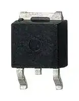


IKD10N60RC2ATMA1
IGBT, 18.8 A, 2 V, 79 W, 600 V, TO-252 (DPAK), 3 Pins
- Manufacturer: INFINEON
- Product type: Single IGBTs
- MSL: MSL 1 - Unlimited
- SVHC: No SVHC (25-Jun-2025)
- No. of Pins: 3Pins
- Product Range: TRENCHSTOP RC
- Power Dissipation: 79W
- Transistor Mounting: Surface Mount
- Transistor Case Style: TO-252 (DPAK)
- Operating Temperature Max: 175°C
- Continuous Collector Current: 18.8A
- Collector Emitter Voltage Max: 600V
- Collector Emitter Saturation Voltage: 2V
| Delivery and price | |
|---|---|
| Units per pack | 5000 |
| Price | 0.401 € |
| Current stock | 200+ |
| Lead time | 30 days |
## Evaluation Board For AURIX™ Family ## AURIX™ lite Kit V2 Document Revision 2.0 ## Board User‘s Manual Revision 2020-10-27 Microcontroller ## **Edition 27. October, 2020** ## **Published by** ## **Infineon Technologies AG** ## **81726 Munich, Germany** ## **© 2020 Infineon Technologies AG All Rights Reserved.** ## **Legal Disclaimer** The information given in this document shall in no event be regarded as a guarantee of conditions or characteristics. With respect to any examples or hints given herein, any typical values stated herein and/or any information regarding the application of the device, Infineon Technologies hereby disclaims any and all warranties and liabilities of any kind, including without limitation, warranties of non-infringement of intellectual property rights of any third party. ## **Information** For further information on technology, delivery terms and conditions and prices, please contact the nearest Infineon Technologies Office ( **www.infineon.com** ). ## **Warnings** Due to technical requirements, components may contain dangerous substances. For information on the types in question, please contact the nearest Infineon Technologies Office. Infineon Technologies components may be used in life-support devices or systems only with the express written approval of Infineon Technologies, if a failure of such components can reasonably be expected to cause the failure of that life-support device or system or to affect the safety or effectiveness of that device or system. Life support devices or systems are intended to be implanted in the human body or to support and/or maintain and sustain and/or protect human life. If they fail, it is reasonable to assume that the health of the user or other persons may be endangered. **AURIX™ lite Kit V2** **==> picture [105 x 46] intentionally omitted <==** |**Revision History**|| |---|---| |**age or Item**|**Subjects(major changes sinceprevious revision)**| |Revision 2020,<br>October|Initial relased Version is V2.0| ## **Trademarks of Infineon Technologies AG** AURIX™, C166™, CanPAK™, CIPOS™, CIPURSE™, EconoPACK™, CoolMOS™, CoolSET™, CORECONTROL™, CROSSAVE™, DAVE™, EasyPIM™, EconoBRIDGE™, EconoDUAL™, EconoPIM™, EiceDRIVER™, eupec™, FCOS™, HITFET™, HybridPACK™, I²RF™, ISOFACE™, IsoPACK™, MIPAQ™, ModSTACK™, my-d™, NovalithIC™, OptiMOS™, ORIGA™, PRIMARION™, PrimePACK™, PrimeSTACK™, PRO-SIL™, PROFET™, RASIC™, ReverSave™, SatRIC™, SIEGET™, SINDRION™, SIPMOS™, SmartLEWIS™, SOLID FLASH™, TEMPFET™, thinQ!™, TRENCHSTOP™, TriCore™. ## **Other Trademarks** Advance Design System™ (ADS) of Agilent Technologies, AMBA™, ARM™, MULTI-ICE™, KEIL™, PRIMECELL™, REALVIEW™, THUMB™, µVision™ of ARM Limited, UK. AUTOSAR™ is licensed by AUTOSAR development partnership. Bluetooth™ of Bluetooth SIG Inc. CAT-iq™ of DECT Forum. COLOSSUS™, FirstGPS™ of Trimble Navigation Ltd. EMV™ of EMVCo, LLC (Visa Holdings Inc.). EPCOS™ of Epcos AG. FLEXGO™ of Microsoft Corporation. FlexRay™ is licensed by FlexRay Consortium. HYPERTERMINAL™ of Hilgraeve Incorporated. IEC™ of Commission Electrotechnique Internationale. IrDA™ of Infrared Data Association Corporation. ISO™ of INTERNATIONAL ORGANIZATION FOR STANDARDIZATION. MATLAB™ of MathWorks, Inc. MAXIM™ of Maxim Integrated Products, Inc. MICROTEC™, NUCLEUS™ of Mentor Graphics Corporation. Mifare™ of NXP. MIPI™ of MIPI Alliance, Inc. MIPS™ of MIPS Technologies, Inc., USA. muRata™ of MURATA MANUFACTURING CO., MICROWAVE OFFICE™ (MWO) of Applied Wave Research Inc., OmniVision™ of OmniVision Technologies, Inc. Openwave™ Openwave Systems Inc. RED HAT™ Red Hat, Inc. RFMD™ RF Micro Devices, Inc. SIRIUS™ of Sirius Satellite Radio Inc. SOLARIS™ of Sun Microsystems, Inc. SPANSION™ of Spansion LLC Ltd. Symbian™ of Symbian Software Limited. TAIYO YUDEN™ of Taiyo Yuden Co. TEAKLITE™ of CEVA, Inc. TEKTRONIX™ of Tektronix Inc. TOKO™ of TOKO KABUSHIKI KAISHA TA. UNIX™ of X/Open Company Limited. VERILOG™, PALLADIUM™ of Cadence Design Systems, Inc. VLYNQ™ of Texas Instruments Incorporated. VXWORKS™, WIND RIVER™ of WIND RIVER SYSTEMS, INC. ZETEX™ of Diodes Zetex Limited. Last Trademarks Update 2011-02-24 EtherCAT® is registered trademark and patented technology, licensed by Beckhoff Automation GmbH, Germany. Revision October, 2020 **AURIX™ lite Kit V2** **==> picture [105 x 46] intentionally omitted <==** ## **Table of Contents** ## **Table of Contents** |**Table**|**Table of Contents**<br>**of Contents**| |---|---| |**1**|**Introduction ............................................................................................................................. 6**| |1.1|Block Diagram ...................................................................................................................................... 7| |**2**|**Hardware Description ............................................................................................................... 8**| |2.1|Power Supply ....................................................................................................................................... 9| |2.2|User Push Buttons, User LEDs and Potentiometer ............................................................................ 10| |2.3|Debugging and on board miniWiggler ............................................................................................... 11| |2.3.1|USB Connector ................................................................................................................................... 11| |2.3.2|Serial Connection to PC ...................................................................................................................... 11| |2.3.3|miniWiggler JDS ................................................................................................................................. 12| |2.4|Reset .................................................................................................................................................. 12| |2.5|CAN Transceiver ................................................................................................................................. 12| |2.6|I2C Eeprom ......................................................................................................................................... 12| |2.7|Ethernet ............................................................................................................................................. 13| |2.8|Optional Cypress Semper™ (Secure) Flash ........................................................................................ 13| |2.9|Optional F-RAM .................................................................................................................................. 13| |**3**|**Configuration .......................................................................................................................... 14**| |3.1|Bootmode .......................................................................................................................................... 14| |3.2|Config Signals ..................................................................................................................................... 14| |3.3|Optional resistors ............................................................................................................................... 15| |**4**|**Connector Pin Assignment ...................................................................................................... 16**| |4.1|Pinout of X1 and X2 connectors ......................................................................................................... 16| |4.2|Shield2Go and MikroBus™ Pinout ..................................................................................................... 17| |4.3|Arduino Compatible Connector ......................................................................................................... 18| |4.4|Infineon DAP Debug Connector (10-pin) ........................................................................................... 19| |**5**|**Schematics and Placement ...................................................................................................... 20**| Revision October, 2020 Board Users Manual 4 **AURIX™ lite Kit V2** **==> picture [105 x 46] intentionally omitted <==** ## **Table of Contents** |**List**|**of**|**Figures**| |---|---|---| |Figure|1|Block Diagram of the AURIX™ lite Kit V2 ............................................................................................. 7| |Figure|2|AURIX™ lite Kit Board V2 View from the Top ....................................................................................... 8| |Figure|3|AURIX™ lite Kit Board V2 View from the Bottom ................................................................................ 8| |Figure|4|Power Supply Concept ....................................................................................................................... 10| |Figure|5|Signal mapping of the pin headers X1 and X2 ................................................................................... 16| |Figure|6|Signal mapping of the pin headers for Mikrobus and Shield2Go Connector 1 and 2 ........................ 17| |Figure|7|Mapping of Arduino Functions to AURIX™ Pin Functions .................................................................. 18| |Figure|8|Schematic: Project Overview ............................................................................................................. 20| |Figure|9|Schematic: On Board miniWiggler ..................................................................................................... 21| |Figure|10|<br>Schematic: Power and Connectors .................................................................................................... 22| |Figure|11|<br>Schematic: CPU and config ................................................................................................................ 23| |Figure|12|<br>Schematic: Ethernet and memory expansion .................................................................................... 24| |Figure|13|<br>Placement: Top View ......................................................................................................................... 25| |Figure|14|<br>Placement: Bottom View ................................................................................................................... 26| |**List**|**of**|**Tables**| |---|---|---| |Table|1|Overview of the Board Specification ................................................................................................... 6| |Table|2|AURIX™ Pin Mapping for User LEDs .................................................................................................. 10| |Table|3|miniWiggler Pin Mapping for User LEDs ........................................................................................... 11| |Table|4|AURIX™ Push Buttons and Potentiometer ........................................................................................ 11| |Table|5|CAN Signals and AURIX™ Pin Mapping.............................................................................................. 12| |Table|6|User Startup Modes ......................................................................................................................... 14| |Table|7|Config Signals .................................................................................................................................... 14| |Table|8|Signal mapping of the optional resistors .......................................................................................... 15| |Table|9|Pin Assignment of the DAP Debug Connector .................................................................................. 19| Revision October, 2020 Board Users Manual 5 **AURIX™ lite Kit V2** **Hardware Description** **==> picture [105 x 46] intentionally omitted <==** ## **1 Introduction** This document describes the features and hardware details of the **AURIX™ lite Kit V2** equipped with a **32-Bit Single-Chip AURIX™ TriCore™-based Microcontroller TC375, TC365, TC275 or TC265** from Infineon Technologies AG. It can be used with a range of development tools including Infineon’s free of charge Eclipse based IDE **AURIX™** ™ **Development Studio** or the Eclipse based **“FreeEntryToolchain”** from Hitecs/PLS/Infineon **.** AURIX Development Studio is a comprehensive environment, including C-Compiler and Multi-core Debugger, Infineon’s low-level driver (iLLD), with no time and code-size limitations that enables editing, compiling and debugging application code. The FreeEntryToolchain is a full C/C++ development environment which has a source-level UDE debugger from PLS included and is also based on Infineon low-level driver (iLLD). Table 1 shows the overview specifications of the whole board. ## **Table 1 Overview of the Board Specification** |CPU Core AURIX™|Manufacturer Order No.|SAK-TC375TP-96F300W AA| |---|---|---| ||Manufacturer Order No.|SAK-TC365DP-64F300W AA| ||Manufacturer Order No.|SAK-TC275TP-64F200W DC| ||Manufacturer Order No.|SAK-TC265D-40F200W BC| |Board Dimensions|66.0 x 131.0 mm|| |Power|<br>on-board miniWiggler Micro-AB USB interface<br><br>external powering 5 V…40 V (recommended 7 V...14 V)|| |Connectors|<br>Most AURIX™ pins available on expansion connectors (X1, X2)<br><br>Two Infineon Shield2Go connectors<br><br>Arduino compatible connectors for 3.3 V<br><br>mikroBUS™ connector<br><br>Micro-USB connector<br><br>DAP Debug connector<br><br>CAN connector<br><br>RJ45 connector|| |Others|<br>CAN transceiver TLE9251VSJ from Infineon<br><br>Low Power 10/100 Mbps Ethernet Physical Layer Transceiver DP83825I from TI<br><br>1 user push-button, 3 user LEDs<br><br>Reset push-button<br><br>Potentiometer(10kOhm)for variable analoginput|| These boards are neither cost nor size optimized and do not serve as a reference design. Revision October, 2020 Board Users Manual 6 **AURIX™ lite Kit V2** **==> picture [105 x 46] intentionally omitted <==** ## **Hardware Description** ## **1.1 Block Diagram** - The block diagram in Figure 1 shows the main components of the AURIX™ lite Kit V2 and their interconnections. **==> picture [480 x 337] intentionally omitted <==** **----- Start of picture text -----**<br> Pin Header X2<br>3.3V<br>DC IN Power 5V 2x20, 0.1"<br>LDO<br>Arduinoä Pin Header (DIGITAL)<br>UART<br>Power 3.3V 3.3V ASCLIN3<br>LDO<br>I2C0<br>P00.7<br>VDD QSPI0<br>12 MHz R35/0R ADC/AN18<br>External L3/3,3µH<br>ADC/AN19<br>Crystal<br>C39/22µF VDD GPIO<br>Ext. Oscillator Power UART<br>Input Interface Ext. Power PORSTN GPIO Dig. Core Port 0 ASCLIN1<br>Octal Bus Input Supply<br>I2C0<br>USB2.0Micro DP/DM UTMIPHY FT2232HLFTDI ChannelMPSSEA Buf fer Gate GateExt. AurixTC275 or TC265ä TC375, TC365, PortADC ADC/AN26QSPI2<br>Ctrl 32,33 GPIO<br>EEPROM MPSSE<br>Interface Channel B 2 x Single-Bit Ext. Osci CAN0 Port 11, 13, UART<br>Bus Tranceiver OCDS Input Node0 14, 15, 20, ASCLIN2<br>21, 22, 23 I2C0<br>ADBUS2<br>2x LEDs QSPI0<br>EEPROM 1kB for OCDS Single Bus ADC/AN16<br>93LC46B-I/SN ACBUS4 Buf fer Gate ADC/AN17<br>ADBUS1 DAP1 ConnectorDAP External20 MHz CAN TranceiverInfineon GPIO<br>P21.7 Crystal TLE9251VSJ<br>EEPROM 2kB<br>24AA02E48-E/OT<br>EUI-48ä Node Address<br>Optional Semper<br>(secure) Flash<br>CAN Header<br>1x2, 0.1"<br>RJ45 Ethernet Phy Optional F-RAM<br>DP83825IRMQR Arduinoä Pin Header (ANALOG IN)<br>Pin Header X1<br>2x20, 0.1"<br>Shield2GO Slot1 S2G2<br>Mikrobus<br>ä<br> Connector<br>Shield2GO Slot1 S2G1<br>QSPI1 GPIO I2C0 ASCLIN0<br>Reset Button Button 1<br>LED1/LED2<br>P00.5/P00.6<br>QSPI1 I2C0 ASCLIN<br>AN24-25 AN36-39<br>**----- End of picture text -----**<br> **Figure 1 Block Diagram of the AURIX™ lite Kit V2** Revision October, 2020 Board Users Manual 7 **AURIX™ lite Kit V2** ## **Hardware Description** ## **2 Hardware Description** The following chapters give a detailed description of the board hardware and how it can be used. The different parts of the kits series are shown in Figure 2 and 3. **Figure 2 AURIX™ lite Kit Board V2 View from the Top** **==> picture [301 x 11] intentionally omitted <==** **----- Start of picture text -----**<br> Figure 3 AURIX™ lite Kit Board V2 View from the Bottom<br>**----- End of picture text -----**<br> Revision October, 2020 Board Users Manual 8 **AURIX™ lite Kit V2** **==> picture [105 x 46] intentionally omitted <==** ## **Hardware Description** ## **2.1 Power Supply** The AURIX™ lite Kit V2 must be supplied by an external DC power supply, this can be done via the DC plug X3 (recommended voltage range +7 V…+14 V) or via the micro USB plug X4 (+5 V). The green Power LED4 indicates the presence of the generated 3.3 V supply voltage. For X3 you can use a female DC supply plug with outside diameter of 5.5 mm and inside diameter of 2.1 mm or 2.5 mm. The inner contact is positive and the outer contact is ground. In case that the board is powered via the micro USB plug X4, the used voltage will be always less than 5 V (~4.5 V) because the USB voltage is protected by a schottky diode (D1). Therefore also it is possible to use X3 and X4 on the same time. As long the voltage on X3 is higher than +7 V the board is powered via X3. If the voltage on X3 is less than +5.5 V the board is powered via X4. Between +5.5 V and +7 V on X3 the board is powered from X3 and X4 together. If the board is powered via a USB plug and/or the DC plug, it’s not recommended to apply an additional power supply to one of the power pins (VEXT, +5V, +3V3, VDD_USB) on the pin headers X1, X2, the Arduino Power header X302, the Shield2GO slots or the mikroBus™ connectors, because there is no protection against reverse current into the external power supply. These power pins can furthermore be used, to power an external circuit and therefore used as an output. But care must be taken to not draw more current than USB can deliver. A PC as USB2.0 host typically can deliver up to 500 mA current and USB3.0 up to 900 mA. For best performance, we recommend to use USB3.0. If higher currents are required and in order to avoid damages on the USB host, the use of an external USB power supply unit, which is able to deliver higher currents, is possible. **Note:** _The LDO G1, that transfers the 5 V to 3.3 V, and LDO G2, that transfers VIN to 5 V, has a maximum output current rating of 1 A. Therefore, the maximum current consumption is limited to 1 A. Do not apply any additional voltage on the supply pins, because they are directly connected to the output of the LDO G1/G2 and further backwards voltage can damage or destroy the LDO. Furthermore, do not apply multiple sources on the power pins, otherwise you risk to damage and destroy the board._ However, more options are possible, but therefore, caution is necessary, to avoid any damage to the board and your supplies. Please ensure that X4 is **not** supplied by any power source or PC, for all mentioned configurations below. Otherwise, **you risk to damage your source or PC** . Ensuring the mentioned points, following supply options are possible with a +5 V power source: - Option 1: Supply +5 V on the +5V pin at X302 Arduino power connector - Option 2: Supply +5 V on either one of the VDD_USB pins at X1 or X2 connector - Option 3: Supply +7 V…+14 V on the VIN pin at X302 Arduino power connector Revision October, 2020 Board Users Manual 9 **AURIX™ lite Kit V2** **==> picture [105 x 46] intentionally omitted <==** **==> picture [107 x 10] intentionally omitted <==** **----- Start of picture text -----**<br> Hardware Description<br>**----- End of picture text -----**<br> **==> picture [497 x 377] intentionally omitted <==** **----- Start of picture text -----**<br> VDD_USB<br>Pin Connector X2<br>+3V3<br>X303 X304<br>U7 DAP<br>CAN Tranceiver<br>Con.<br>R32<br>D5<br>Potentiometer<br>+5V VDD_USB<br>U6 VEXT +3V3 G1<br>Aurixä D1 X4<br>TC3X5 or TC2X5 +3V3 LDO In Micro<br>Infineon<br>Microcontroller Out IFX27001TFV33 USB<br>S2G1/S2G2<br>IC1 On Board 3V3 5V G2 VIN D2 X3<br>U1 - U5 miniWiggler S2Go Slots R39/0R_opt +5V LDO DC<br>Infineon<br>Out IFX27001TFV50 In plug<br>U9 I2C Eeprom 3V3 5V<br>mikroBusä<br>U8 10M / 100M<br>Ethernet<br>U10 Optional VIN VEXT +5V +3V3<br>External Flash<br>+3V3<br>U11 Optional Arduino Power Connector X302 X301<br>External F-RAM<br>VDD_USB<br>Pin Connector X1<br>Figure 4 Power Supply Concept<br>R27/0R<br>**----- End of picture text -----**<br> **Note:** _Do_ _**not** apply any voltage on the mentioned power pins, if the USB is plugged in or any voltage is applied via DC plug. Furthermore, do not apply multiple sources on the power pins, otherwise you risk to damage and destroy the board._ ## **2.2 User Push Buttons, User LEDs and Potentiometer** The **AURIX™ lite Kit V2** provides one user push button, a reset button, two LEDs and one potentiometer. Additionally, LED3 can be used for visualizing an emergency stop function at ESR0 (emergency service request). The LEDs LED5 and LED6 are used for visualizing activites via the on-board miniWiggler. The port pins used can be found in Table 2 and Table 4. **Table 2 AURIX™ Pin Mapping for User LEDs** |**ame**|**AURIX™ Pin**|**Color**|**Active**| |---|---|---|---| |ED1|P00.5|green|Low-active(pull against GND)| |ED2|P00.6|green|Low-active(pull against GND)| |ED3|ESR0|red|Low-active(pull against GND)| Revision October, 2020 Board Users Manual 10 **AURIX™ lite Kit V2** **==> picture [105 x 46] intentionally omitted <==** ## **Hardware Description** |**Table 3**|**miniWiggler Pin Mapping for User LEDs**|**miniWiggler Pin Mapping for User LEDs**|| |---|---|---|---| |**ame**|**miniWiggler Pin**|**Color**|**Active**| |ED5|ADBUS4(ACTIV)|green|Low-active(pull against GND)| |ED6|ADBUS7(RUN)|green|Low-active(pull against GND)| ## **Table 4 AURIX™ Push Buttons and Potentiometer** |**Table 4**|**AURIX™ Push Buttons and**|**Potentiometer**| |---|---|---| |**ame**|**AURIX™ Pin**|**Active**| |utton1|P00.7|Low-active(pull against GND)| |eset|/PORST|Low-active(pull against GND)| |32(10kΩ)*|AN0|-| *Note: Desoldering resistor R33, enables AN0 for other functions, but disables the Potentiometer functionality. ## **2.3 Debugging and on board miniWiggler** The **AURIX™ lite Kit V2** supports debugging via 2 different channels: - On-board miniWiggler via the the microUSB X4 - 10-pin DAP Connector ## **2.3.1 USB Connector** The USB connector is used for connection to a PC. Via the USB it is possible to power the board, using the ASCLIN0 as serial connection via USB and Debugging via DAS. ## **NOTE: Before connecting the board to the PC, make sure that the actual DAS software is installed on the PC.** For actual DAS software please contact your local FAE. The software can also be found on: ## DAS website ## **2.3.2 Serial Connection to PC** After the first connection of USB to a PC the needed driver will be installed automatically. During this there will be created a new COM port on PC. This COM port can be used to communicate with the board via ASCLIN0 of the device and ASCLIN4 (TC3X5 only) if R44 and R45 are assembled. Per default the ASCLIN0 is used on P14.0 and P14.1 (e.g. Generic Bootstrap Loader). Because ASCLIN0 is used also for the Arduino pins, you can use here also ASCLIN4 to use it in parallel, make sure that P14.0/P14.1 are not configured in this case. Revision October, 2020 Board Users Manual 11 **AURIX™ lite Kit V2** **Hardware Description** **==> picture [105 x 46] intentionally omitted <==** ## **2.3.3 miniWiggler JDS** The miniWiggler JDS is a low cost debug interface which allows you access to the device via DAP. Make sure that you have the latest DAS release. Debugging is possible via the DAS Server ‘UDAS‘. Please contact your preferred debug vendor for support of DAS. If you have connected the board to the PC and there runs the DAS server, then a working connection is visible via the green LED5 (ADBUS4). The status LED6 (ADBUS7/green) is switched on/off through the DAS Server, depending on the used debugger (client). ## **IMPORTANT: Make sure that there is no or a tristated connection on the DAP connector if the LED5 (miniWiggler in use) is on.** ## **2.4 Reset** The power on reset input pin (/PORST) of the AURIX™ family is a bi-directional input/output intended for external triggering of power-related resets. If the PORST pin remains asserted after a power event then the reset will be extended until it is deasserted. This does not replace the ESR pins functional reset. An internal pull-up resistor (2.2 kΩ) keeps the PORST# pin high during normal operation. A low level at this pin will force a hardware reset. In case of a MCU internal reset the PORST# pin will drive a low signal. A reset signal can be issued by - the on-board Reset Button (“RESET”) - the on-board miniWiggler via IC FT2232HL (IC1.27 – ACBUS1) - the on-board DAP connector (DAP.10) - the Arduino Power Header (X302.3, “/PORST”) - the pin header X1 (X1.30, “/PORST”) An AURIX™ internal circuit always ensures a save Power-on-Reset. AURIX™ lite Kit V2 does not require any additional external components to generate a reset signal during power-up. For more informations, please refer to the datasheet or user manual of the assembled AURIX™ device. ## **2.5 CAN Transceiver** The **AURIX™ lite Kit V2** provides a CAN interface via the CAN connector. The TLE9251V is the latest Infineon high-speed CAN transceiver generation, used inside HS CAN networks for automotive and also for industrial applications. It is designed to fulfill the requirements of ISO 11898-2 (2016) physical layer specification and respectively also the SAE standards J1939 and J2284. The CAN buses (signals CANH, CANL) are terminated with by a 120 Ohm resistor. The transceiver is connected to the TriCore™ device. To use the CAN pins see Table 5. |**able 5**|**CAN Signals and AURIX™ Pin Mapping**|**CAN Signals and AURIX™ Pin Mapping**|| |---|---|---|---| |**Signal**<br>**Name**|**Pin No. at CAN Pin**<br>**Header**|**AURIX ™Pin, AURIX™ Function**|**Ass. Reg./**<br>**I/O Line**| |CANH|1|-|-| |CANL|2|-|-| |CAN_TX|-|P20.8,CAN node 0 output|TXDCAN0| |CAN_RX|-|P20.7,CAN node 0 input|RXDCAN0B| ## **2.6 I2C Eeprom** The **AURIX™ lite Kit V2** provide a 2 Kb I2C Serial EEPROM with Pre-Programmed EUI-48™ MAC ID (Microchip 24AA02E48). The slave address of this EEPROM is fixed 0x50. The upper half of the array (80hFFh) is permanently write-protected. Write operations to this address range are inhibited. Read operations are not affected. This upper half contains the preprogrammed EUI-48™ node address which can be used as MAC ID for Ethernet. The other 128 bytes are writable and usable by the user. Revision October, 2020 Board Users Manual 12 **AURIX™ lite Kit V2** **Hardware Description** **==> picture [105 x 46] intentionally omitted <==** ## **2.7 Ethernet** The **AURIX™ lite Kit V2** provide a RJ45 connector (X5) for twisted pair ethernet connections.The board use a DP83825I Low Power 10/100 Mbps Ethernet Physical Layer Transceiver from Texas Instruments as physical interface device. For more information about the ethernet modul see AURIX™ User’s Manual, about the PHY see the DP83825I datasheet from TI website. For the connection between AURIX™ and PHY is used RMII. For the MD connection (e.g. for PHY configuration) there is used P21.2 and P21.3. ## **2.8 Optional Cypress Semper™ (Secure) Flash** The **AURIX™ lite Kit V2** provide the possibility to assemble an external flash. Usable devices are Cypress Semper™ NOR Flash Device Family S25HL and Cypress Semper™ Secure NOR Flash Device Family S35HL in - SOIC-16 package. For more information about the flashs please see https://www.cypress.com/products/semper nor-flash-memory and https://www.cypress.com/event/semper-secure-nor-flash-memories. If you assemble a flash then assemble also the ceramic capacitor C64 with 100 nF (size 0603) and the resistor R67 with 0 Ω (size 0603). In case of use a Semper™ Secure NOR Flash you can also assemble the resistor R67 with 0 Ω (size 0603) to connect the interrupt output of the flash to the AURIX™ pin P20.9 (SCU_REQ7 on TC3X5; SCU_REQ11 on TC2X5). The AURIX™ support only single SPI protocol, Dual and Quad SPI protocol is not possible. The flash is connected to P22.0, P22.1, P22.3 (QSPI4 on TC3X5; QSPI3 on TC2X5). Pin P22.2 (Slave Select Output 3 of QSPI4 on TC3X5; Slave Select Output 12 of QSPI3 on TC2X5) is used as slave select. Please note that the used QSPI is shared with the optional F-RAM (see Optional F-RAM). ## **2.9 Optional F-RAM** The **AURIX™ lite Kit V2** provide the possibility to assemble an external serial F-RAM. Usable devices are Cypress F-RAM FM25VN10-G and Cypress F-RAM Serie CY15B in SOIC-8 package. For more information about the F-RAMs please see https://www.cypress.com/products/f-ram-nonvolatile-ferroelectric-ram. If you assemble F-RAM then assemble also the ceramic capacitor C65 with 100 nF (size 0603). The F-RAM is connected to P22.0, P22.1, P22.3 (QSPI4 on TC3X5; QSPI3 on TC2X5). Pin P23.1 (Slave Select Output 6 of QSPI4 on TC3X5; Slave Select Output 13 of QSPI3 on TC2X5) is used as slave select. Unfortunately there is no connection on pin 3 (#WP) and pin 7 (#HOLD) of the F-RAM. Please check the datasheet if the used F-RAM has internal weak pull-up connected or need an external connection to VDD. If external connection is needed then make such a connection via wire wrap line. Please note that the used QSPI is shared with the optional flash (see Optional Cypress Semper™ (Secure) Flash). Revision October, 2020 Board Users Manual 13 **AURIX™ lite Kit V2** **==> picture [105 x 46] intentionally omitted <==** ## **Hardware Description** ## **3 Configuration** ## **3.1 Bootmode** ## **Table 6 User Startup Modes[1)2)]** |**able 6**<br>**User**|**Startup Modes1)2)**|||| |---|---|---|---|---| |**HWCFG[5...3]**|**Type of Boot**|**R58**|**R57**|**R59**| |XX1|Start-up mode is selected by Boot Mode Index|X|X|NA| |110|Internal Start from Flash|NA|NA|A| |100|Alternate Boot Mode, Generic Bootstrap Loader on fail<br>(P14.0/P14.1)|A|NA|A| |000|Generic Bootstrap Loader (P14.0/P14.1)|A|A|A| 1) The shadowed line indicates the default setting. 2) ‘A’ means assembled, ‘NA’ means not assembled, ’x’ represents the don’t care state. ## Please see also Table 8. ## **3.2 Config Signals** |**able 7**|**Config Signals**|| |---|---|---| |**Short**<br>**Name**|**Description**|**Comment**| |P14.6|HWCFG0 (LDO / DCDC)|Only with TC2X5, resistor R30 (4.7 kΩ/0603<br>imp) pulls signal against GND (DCDC) and is<br>assembled initially if board is using TC2X5.| |P14.5|HWCFG1 (EVR33ON / EVR33OFF)|Resistor R31 (4.7 kΩ/0603 imp) pulls signal<br>against GND (EVR33OFF) and is assembled<br>initially.| |P14.2|HWCFG2 (EVRCON / EVRCOFF)|Resistor R52 (4.7 kΩ/0603 imp) must be<br>assembled if R59 is assembled (GPIOs are set<br>to tri-state) and TC2X5 is used (TC3X5 has<br>internal pull-up).| |P14.3|HWCFG3(see boot configurationTable 6)|-| |P10.5|HWCFG4(see boot configurationTable 6)|-| |P10.6|HWCFG5(see boot configurationTable 6)|-| |P14.4|HWCFG6 (GPIOs pull-up / tri-state)|Resistor R59 (4.7 kΩ/0603 imp) pulls signal<br>against GND (GPIOs in tri-state after reset) and<br>and is not assembled initially.| Revision October, 2020 Board Users Manual 14 **AURIX™ lite Kit V2** **Hardware Description** **==> picture [105 x 46] intentionally omitted <==** ## **3.3 Optional resistors** Some resistors/bridges enable/disable or changing functions of specific signals in Table 8. To disable the signals, the resistors have to be removed. To enable, the resistor has to be assembled. **For example** : Desoldering the intialy assembled resistor R33, disables the Potentiometer and the analog Signal AN0 of the AURIX™, making it usable for other purposes. ## **Table 8 Signal mapping of the optional resistors** |**Resistor**|**Res.**|**Assembled**|**Signal**|**Size**<br>**(imperial)**|**Comment**| |---|---|---|---|---|---| |R33|0 Ω|yes|AN0|0603|Disassemble to disable the potentiometer| |R37|0 Ω|yes|XTAL2|0603|Serial<br>resistor<br>to<br>reduce<br>oscillator<br>amplitude if needed.| |R39|0 Ω|no|+5V|0603|Assemble to connect 5V to Mikrobus and<br>Shield2Go connector| |R59|4.7 kΩ|no|HWCFG6/P14.4|0603|Assemble to disable the internal pull-ups<br>with power on| |R52|4.7 kΩ|No|HWCFG2/P14.2|0603|Assemble to enable the EVR13, only<br>needed with TC2X5 and R59 assembled| |R53|4.7 kΩ|no|HWCFG3/P14.3|0603|Assemble to boot from BMI, only needed<br>with TC2X5 and R59 assembled| |R56|4.7 kΩ|no|HWCFG3/P14.3|0603|Assemble<br>to<br>select<br>boot<br>from<br>HWCFG4/5, valid setting on P10.5/P10.6<br>needed| |R54|4.7 kΩ|no|HWCFG4/P10.5|0603|Set HWCFG4 to high, only needed with<br>R56 assembled, not with R57| |R55|4.7 kΩ|no|HWCFG5/P10.6|0603|Set HWCFG5 to high, only needed with<br>R56 assembled, not with R58| |R57|4.7 kΩ|no|HWCFG4/P10.5|0603|Set HWCFG4 to low, only needed with<br>R56 assembled, not with R54| |R58|4.7 kΩ|no|HWCFG5/P10.6|0603|Set HWCFG5 to low, only needed with<br>R56 assembled, not with R55| |R44|0 Ω|no|P14.1, P00.12|0603|Assemble to use ASCLIN4 (P00.12)<br>instead of ASCLIN0 (P14.1) via USB,<br>only with TC3X5, P14.1 not usable in this<br>case| |R45|0 Ω|no|P14.0, P00.9|0603|Assemble to use ASCLIN4 (P00.9)<br>instead of ASCLIN0 (P14.0) via USB,<br>only with TC3X5, P14.0 not usable in this<br>case| Revision October, 2020 Board Users Manual 15 **AURIX™ lite Kit V2** **==> picture [105 x 46] intentionally omitted <==** ## **Hardware Description** ## **4 Connector Pin Assignment** ## **4.1 Pinout of X1 and X2 connectors** The pin headers X1 and X2 can be used to extend the evaluation board or to perform measurements on the AURIX™ TC3X5/TC2X5. Figure 5 shows the available GPIOs / signals at these pin headers. The pin table is also printed onto the bottom side of the PCB. ||**Pin Header X1**|**Pin Header X1**|**Pin Header X1**|**Pin Header X1**||||**Pin Header X2**|**Pin Header X2**|**Pin Header X2**|**Pin Header X2**|| |---|---|---|---|---|---|---|---|---|---|---|---|---| ||GND|1|2||+3V3|||GND|1|2|VDD_USB|| ||P33.11|3|4||P33.12|||P00.0|3|4|P00.1|| ||P33.13|5|6||P32.41)|||P00.2|5|6|P00.3|| ||P23.1|7|8||P23.0||LED2|P00.6|7|8|P00.5|LED1| ||P23.3|9|10||P23.2|||P00.8|9|10|P00.7|Button1| |RST_S2G2|P23.5|11|12||P23.4|RST_S2G1||P00.10|11|12|P00.9|| ||P22.1|13|14||P22.0|||P00.12|13|14|P00.11|| ||P21.0|15|16||P22.2|||VAREF1|15|16|AN47|| |MDC|P21.2|17|18||P22.3|||AN46|17|18|AN45|| ||P21.4|19|20||P21.3|MDIO||AN44|19|20|AN7|| |SPICLK_S2G|P20.10|21|22||P21.5|||AN6|21|22|AN5|| |TXD_S2G2|P20.0|23|24||P20.1|||AN4|23|24|AN3|| |RXD_S2G2|P20.3|25|26||/ESR1|ESR1||AN2|25|26|AN1|| |ESR0|/ESR0|27|28||P20.14|MOSI_S2G|Potentiometer|AN0|27|28|P33.0|| ||P15.5|29|30||/PORST|Reset||P33.1|29|30|P33.2|| ||P15.4|31|32||P11.12|CLK50||P33.3|31|32|P33.4|| |CRS_DV|P11.11|33|34||P11.10|RX_D0||P33.5|33|34|P33.6|| |RX_D1|P11.9|35|36||P11.6|TX_EN||P33.7|35|36|P33.8|RXD_S2G1| |TX_D0|P11.3|37|38||P11.2|TX_D1|TXD_S2G1|P33.9|37|38|P33.10|| ||VDD_USB|39|40||GND|||+3V3|39|40|GND|| **Figure 5 Signal mapping of the pin headers X1 and X2** Note: 1) Different signal compared with AURIX™ TC275 lite Kit V1.x Revision October, 2020 Board Users Manual 16 **AURIX™ lite Kit V2** **Hardware Description** **==> picture [105 x 46] intentionally omitted <==** ## **4.2 Shield2Go and MikroBus™ Pinout** The pin connectors for the Shield2Go Connectors 1 and 2 and the mikroBus™ can be used to extend the evaluation board or to perform measurements on the AURIX™ TC3X5/TC2X5. Figure 6 shows the available signals at these connectors. The pin table is also printed onto the top and bottom side of the AURIX™ lite Kit V2. ## **Shield2Go Connector 1 Shield2Go Connector 2** |**AURIX™**<br>**Pins**<br>RX<br>P33.8<br>TX<br>P33.9<br>RST/GPIO2<br>P23.41)<br>GPIO1<br>P32.2<br>CS<br>P20.131)<br>SCLK<br>P20.111)<br>MOSI<br>P20.141)<br>MISO<br>P20.121)|<br> <br>10<br> <br>11<br> <br>12<br> <br>13<br> <br>14<br> <br>15<br> <br>16<br> <br>17<br>|**AURIX™**<br>**Pins**<br>1<br>+5V<br>5V<br>2<br>AN18<br>AN1<br>3<br>AN19<br>AN2<br>4<br>P13.22)<br>SDA<br>5<br>P13.12)<br>SCL<br>6<br>GND<br>GND<br>7<br>+3V3<br>3V3<br>8<br>P10.8<br>INT/GPIO3<br>9<br>P14.101)<br>PWM/GPIO4|**AURIX**<br>**™ Pins**<br>RX<br>P20.310<br>TX<br>P20.0 11<br>RST/GPIO2<br>P23.51)12<br>GPIO1<br>P32.3 13<br>CSP20.101) 14<br>SLCKP20.111) 15<br>MOSIP20.141)16<br>MISOP20.121) 17|**AURIX**<br>**™ Pins**<br>RX<br>P20.310<br>TX<br>P20.0 11<br>RST/GPIO2<br>P23.51)12<br>GPIO1<br>P32.3 13<br>CSP20.101) 14<br>SLCKP20.111) 15<br>MOSIP20.141)16<br>MISOP20.121) 17| |---|---|---|---|---| |||1||| ||10|2||10| ||11|3||11| ||12|4||12| ||13|5||13| ||14|6||14| ||15|7||15| ||16|8||16| ||17|9||17| ||**mikroBus™ Connector**|**mikroBus™ Connector**||| |---|---|---|---|---| |1|AN26<br>AN|PWM|P2.8|16| |2|P10.6<br>RST|INT|P10.7|15| |3|P14.71)CS|RX|P15.1|14| |4|P15.81) SCK|TX|P15.0|13| |5|P15.71)MISO|SCL|P13.12)|12| |6|P15.61)MOSI|SDA|P13.22)|11| |7|+3V3<br>3.3V|5V|+5V|10| |8|GND<br>GND|GND|GND|9| ## **Figure 6 Signal mapping of the pin headers for Mikrobus and Shield2Go Connector 1 and 2** Note:[1)] Different signal compared with AURIX™ TC275 lite Kit V1.x - [2)] The I2C buses SCL and SDA are shared on the Shield2GOs, mikroBus™, Arduino connectors and the I2C eeprom. Revision October, 2020 Board Users Manual 17 **AURIX™ lite Kit V2** **Hardware Description** **==> picture [105 x 46] intentionally omitted <==** ## **4.3 Arduino Compatible Connector** The mapping of GPIOs and AURIX™ pin functions to Arduino compatible functions can be found in Figure 6. The Arduino compatible connector supports - SPI interface (SPI_xxx) - I2C interface (I2C_xxx) - UART interface (UART_xxx) - PWM signal outputs (PWM0-13) - ADC input (ADC0-5) - Interrupt input (INT0-1) Note that all pins are cabable of offering more functions than mentioned in Figure 6. For more information about all pin functions, we want to refer you to the corresponding datasheet. **==> picture [472 x 291] intentionally omitted <==** **----- Start of picture text -----**<br> (Top View)<br>10 P13.1 I2C_SCL: I2C0_SCL0<br>9 P13.2 I2C_SDA: I2C0_SDA0<br>8 VAREF AREF: VAREF2/VAREF1<br>7 GND SPI - Master Mode<br>6 P10.2 SPI_CLK: QSPI1.SLK1 PWM13 : GTM.TOUT104<br>N.C. 1<br>5 P10.1 SPI_MISO: QSPI1.MRST1A PWM12 : GTM.TOUT103<br>VEXT/3.3V IOREF 2<br>4 P10.3 SPI_MOSI: QSPI1.MTSR1 PWM11 : GTM.TOUT105<br>/PORST RESET 3<br>3 P10.5 SPI_CS: QSPI1.SLSO19 PWM10 : GTM.TOUT107<br>+3V3 3.3V 4<br>PWM9: GTM.TOUT7 /<br>+5V +5V 5 2 P02.7 CCU60.CC61<br>PWM8: GTM.TOUT6 /<br>GND 6 1 P02.6 IO2: P02_IN.P / P02_OUT.P6 CCU60.CC60<br>GND 7<br>PWM7: GTM.TOUT4 /<br>VIN VIN 8 8 P02.4 IO1: P02_IN.P4 / P02_OUT.P4 CCU60.CC62<br>PWM6: GTM.TOUT5 /<br>7 P02.5<br>CCU60.COUT62<br>ADC0: AN39 / VADCG4.7 P40.9 1 6 P02.3 PWM5: GTM.TOUT3 /<br>CCU60.COUT61<br>ADC1: AN38 / VADCG4.6 P40.8 2 5 P10.4 IO0: P10_IN.P4 / P10_OUT.P4 PWM4: GTM.TOUT106<br>ADC2: AN37 / VADCG4.5 P40.7 3 4 P02.1 INT1: ERS2.REQ14 (ERU) PWMCCU60.COUT603: GTM.TOUT1 /<br>ADC3: AN36 / VADCG4.4 P40.6 4 3 P02.0 INT0: ERS3.REQ6 (ERU) PWM2:CCU60.CC60 GTM.TOUT0 /<br>ADC4: AN24 / VADCCG3.0 P40.0 5 2 P15.2 UART_TXD: ASCLIN0.ATX0 PWM1: GTM.TOUT73<br>ADC5: AN25 / VADCG3.1 P40.1 6 1 P15.3 UART_RXD: ASLIN0.ARX0B PWM0: GTM.TOUT74<br>X303<br>X302<br>POWER<br>X304<br>X301<br>DIGITAL<br>ANALOG IN<br>**----- End of picture text -----**<br> **Figure 7 Mapping of Arduino Functions to AURIX™ Pin Functions** The **AURIX™ lite Kit V2** works with 3.3 V logic levels. Therefore, any board that works with 5 V logic levels, cannot be used. Analog input signals ADC0-5 are limited to a voltage which is smaller or equal than VAREF with VAREF = VDDM = 3.3 V. Primarily, ADC0 to ADC5 should be used as analog input, because there is no additional circuit connected to these pins. Parallel operation of I2C and ADC4 / ADC5 is possible, because they don’t share anymore the same pins at the Arduino connector X301 and X303 as on previous AURIX™ lite Kit V1. Revision October, 2020 Board Users Manual 18 **AURIX™ lite Kit V2** **Hardware Description** **==> picture [105 x 46] intentionally omitted <==** ## **4.4 Infineon DAP Debug Connector (10-pin)** Infineon’s 10-pin Device Access Port Debug Connector (DAP) is a two-wire tool access port for microcontrollers and similar devices. It allows robust high speed connections over a long cable for automotive applications. The pin assignment of the DAP Debug Connector is shown in Table 9. The board comes with a DAP connector. You can connect a DAP hardware here. If you use this connector make sure that the miniWiggler JDS is not activ (LED5 is off). For more information, we refer you to the DAP Connector Manual. **Table 9 Pin Assignment of the DAP Debug Connector** |**Pin**|**Name**|**AURIX™ Pin**|**Direction**|**Description**| |---|---|---|---|---| |1|VREF|VEXT|O|Supply voltage from the target system. The voltage has to be<br>strong enough to supply the target side of the level shifters within<br>the tool hardware up to about 20 MHz DAP operating frequency.<br>The required supply current is in the range of 5 mA, mainly<br>caused by signal switching. It can be reduced by lowering<br>frequency and capacitance. Beyond 20 MHz the tool hardware<br>has to supply the level shifter from another source and use this<br>pinjust as a voltage reference| |2|**DAP1**<br>SPD<br>UART|TMS|IO|DAP: Datapin.| ||||IO|SPD: Datapin.| ||||IO|Single-wire UART. Serial communication interface (e.g. used for<br>BootstrapLoader BSL).| |3|GND|GND||Recommended pin for signal return of DAP1 for high frequency<br>impedance matching.| |4|**DAP0**<br>SUP|TCK|I|DAP: Clock.| ||||I|SPD: Optional user pin value for feedback into the target system.<br>Otherwise reserved| |5|GND|GND||Recommended pin for signal return of DAP0 for high frequency<br>impedance matching.| |6|**DAP2**<br>USER0|P21.7|IO|DAP: Optional second datapin.| ||||IO/O|Generic signal that can be used for non specified functions.| |7|KEY (GND<br>in cable)|GND|-|If the recommended connector with keying shroud is not used,<br>this pin provides another option to enforce polarization. In that<br>instance this pin is removed from the target connector and the<br>associated jack in the cable connector closed with a plastic pin for<br>example.| |8|**DAP3**<br>USER1<br>(DAPEN)|/TRST|IO|DAP: Optional third datapin.| ||||IO/I|Generic signal that can be used for non-specified functions.| ||||I|Optional indicator that the tool is connected. This can be used to<br>enable the DAP interface of the device| |9|GND|GND||Supply ground.| |10|RESET|/PORST|IO|Target reset signal. Open drain active low signal. May be used bi-<br>directionally to drive or sense the target reset signal. Usually<br>driven by the tool to reset the target system. The target system is<br>responsible for providing a pull-up to VREF on this signal to<br>establish a logic one. The resistor shall not have a value less than<br>1 kOhms.| Revision October, 2020 Board Users Manual 19 **AURIX™ lite Kit V2** ## Cinfineon ## **Hardware Description** **==> picture [245 x 12] intentionally omitted <==** **----- Start of picture text -----**<br> 5 Schematics and Placement<br>**----- End of picture text -----**<br> **==> picture [459 x 663] intentionally omitted <==** **----- Start of picture text -----**<br> Figure 8 Schematic: Project Overview<br>A B C D<br>5<br><Appr.> Rev. V2.0 of<br>Page(s)<br>8 Approved Rel. H.D. Not in version control Sheet1 8<br>SVN Revision:<br>Description Infineon Technologies AG Infineon Technologies AG Am Campeon 1-15 - 85579 Neubiberg - Germany 13:15:09<br>7 First new design for A2G AURIX™ Lite Kit V2 [No Variations] Document Name 01_Revision_History.SchDoc Time: 7<br>Revision History H.D. 16.10.2020<br>Author H.D. Title Variant Size: A3 Author: Date: © Infineon Technologies AG 2020. All Rights Reserved.<br>Date 06/2020<br>Rel.<br>6 07/2020 6<br>Rev. V2.0<br>5 5<br>V2.0 LEGAL DISCLAIMER THE INFORMATION GIVEN IN THIS DOCUMENT IS GIVEN FOR ILLUSTRATING PURPOSES ONLY. THE RECIPIENT OF THIS DOCUMENT MUST VERIFY ANY FUNCTION DESCRIBED HEREIN IN THE REAL APPLICATION. INFINEON TECHNOLOGIES HEREBY DISCLAIMS ANY AND ALL WARRANTIES AND LIABILITIES OF ANY KIND (INCLUDING WITHOUT LIMITATION WARRANTIES OF NON-INFRINGEMENT OF INTELLECTUAL PROPERTY RIGHTS OF ANY THIRD PARTY) WITH RESPECT TO ANY AND ALL INFORMATION GIVEN IN THIS DOCUMENT.<br>4 [No Variations] 4<br>01_Revision_History.SchDoc<br>AURIX™ Lite Kit V2<br>3 3<br>Infineon Technologies AG Infineon Technologies AG Am Campeon 1-15 - 85579 Neubiberg - Germany<br>2 2<br>Index Schematics Page Name Cover Sheet / Revision History OCDS Power_a_Connector CPU Ethernet_Memory_Expansion<br>1 1<br>Page 01 02 03 04 05 06 07 08 09 10<br>A B C D<br>**----- End of picture text -----**<br> Revision October, 2020 Board Users Manual 20 **AURIX™ lite Kit V2** ## Cinfineon ## **Hardware Description** **==> picture [472 x 660] intentionally omitted <==** **----- Start of picture text -----**<br> - (uf<br>a e Pt<br>|<br>)<br>, i<br>AURIX™ Lite Kit V2<br>BDBUS0 BDBUS1<br>A B C D<br>5<br>GND GND DAP1 GND P21.7 <Appr.> Rev. of<br>8 TP1 opt C18 100nF C21 100nF Approved Rel. Not in version control Sheet2 8<br>GND TP2 opt GND GND<br>C13 100nF ADBUS2 +3V3 6 2 4 +3V3 6 2 4<br>3 4 SVN Revision:<br>+3V3 20 10 DAP018 16TRST/ USR014 USR812 9 PORST/7 5 3 GND Y VCCB GND B VCCB GND B<br>VCC GND 1Y1 1Y2 1Y3 1Y4 2Y1 2Y2 2Y3 2Y4 VCC OE_N A VCCA 0DIR1 A VCCA 0DIR1 A<br>U2 SN74LVC1G125DBVR U3 SN74LVC1T45DBVR U4 SN74LVC1T45DBVR<br>+3V3 +3V3 5 1 2 1 5 3 1 5 3 Infineon Technologies AG 13:15:55<br>S4 S7<br>7 2 2 U1 1OE_N 2OE_N 1A1 1A2 1A3 1A4 2A1 2A2 2A3 2A4 SN74AHC244PWR Time: 7<br>LED5 1 Green LED6 1 Green +3V3 R3R13 10k10k 1 19 2 4 6 8 11 13 15 17 GND +3V3C16 100nFACBU ADBUS1 +3V3C17 100nFACBUS5 ADBUS2R18 4.7k GND +3V3C20 100nFACBU ACBUS3R19 4.7k GND Document Name 02_OCDS.SchDoc H.D. 16.10.2020<br>+3V3 ADBUS0 ACBUS2 ADBUS6 ACBUS5<br>Title Variant Size: Author: Date: © Infineon Technologies AG 2020. All Rights Reserved.<br>R1 680R R2 680R DBUS4A ACBUS1 GND GND GND<br>LEDs of OCDS ADBUS7 ADBUS4 Signal Network Switches +3V3 R9 10k<br>6 6<br>+3V3 P00.12 P00.9<br>L2 MMZ1608R300ATA00 R44 0R_opt R45 0R_opt<br>ADBUS0<br>5 5<br>C5 4.7uF R8 10k<br>GND<br>GND<br>C4 100nF<br>ADBUS0 ADBUS1 ADBUS2 ADBUS3 ADBUS4 ADBUS6 ADBUS7 ACBUS1 ACBUS2 ACBUS3 ACBUS4 ACBUS5 ACBUS7 P14.1 P14.0<br>GND<br>16 17 18 19 21 22 23 24 26 27 28 29 30 32 33 34 38 39 40 41 43 44 45 46 48 52 53 54 55 57 58 59<br>IC1<br>ADBUS0 ADBUS1 ADBUS2 ADBUS3 ADBUS4 ADBUS5 ADBUS6 ADBUS7 ACBUS0 ACBUS1 ACBUS2 ACBUS3 ACBUS4 ACBUS5 ACBUS6 ACBUS7 BDBUS0 BDBUS1 BDBUS2 BDBUS3 BDBUS4 BDBUS5 BDBUS6 BDBUS7 BCBUS0 BCBUS1 BCBUS2 BCBUS3 BCBUS4 BCBUS5 BCBUS6 BCBUS7 FT2232HL<br>C11 3.3uF<br>02_OCDS.SchDoc +1V8<br>4 +3V3 Channel A Channel B 4<br>GND<br>+3.3V USB Interface Misc Signal Group EEPROM Interface<br>+3V3<br>i<br>Power<br>+1.8V<br>0nF 0nF 0nF 0nF +1V8 0nF 0nF 0nF DP DM RESET_N REF OSCI OSCO TEST PWREN_N SUSPEND_N EECS EECLK EEDATA<br>3 10C1 C610 10C7 10C8 10C9 10C10 10C12 8 7 14 6 2 3 13 60 36 63 62 61 3<br>D_P D_N k1 12k GND<br>GND GND R6 R7 C15 8pF<br>GND<br>C3 100nF GND 22R 2R2 1 2<br>C2 4.7uF R4 R5 Y1 3 4 12MHz +3V3R11 10k R12 10k R14 10k<br>GND<br>2 +3V3 GND +3V3 8 1 2 3 2<br>C14 8pF GND VCC CS CLK DI<br>R17 2.2k<br>USB_D_P USB_D_N VSS NC1 NC2 DO<br>U5 93LC46B-I/SN<br>L1 MMZ1608R300ATA00 GND VDD_USB 5 6 7 4<br>i C100 100nF C19 100nF<br>Power<br>+3V3<br>+3V3 GND<br>USB Connector X4 MP6 MP5 MP4 5 4 3 2 1 MP3 MP2 MP1 R106 1MEG GND<br>1 OCDS 1<br>A B C D<br>V2.0<br>H.D.<br>Infineon Technologies AG Am Campeon 1-15 - 85579 Neubiberg - Germany<br>[No Variations]<br>A3<br>FT2232HL<br>UART /FIFO IC<br>DUAL HIGH SPEED USB<br>1 2<br>49 VREGOUT<br>50 VREGIN<br>5642312049 VCCIOVCCIOVCCIOVCCIOVPLLVPHY AGNDGNDGNDGNDGNDGNDGNDGNDGND 1511135251554710<br>643712 VCOREVCOREVCORE<br>1 2<br>ZX62-AB-5PA(31)<br>**----- End of picture text -----**<br> **==> picture [222 x 11] intentionally omitted <==** **----- Start of picture text -----**<br> Figure 9 Schematic: On Board miniWiggler<br>**----- End of picture text -----**<br> Revision October, 2020 Board Users Manual 21 **AURIX™ lite Kit V2** ## **Hardware Description** **==> picture [472 x 680] intentionally omitted <==** **----- Start of picture text -----**<br> ie A<br>Figure 10 Schematic: Power and Connectors<br>A B C D<br>5<br>8 +3V3 R36 680R LED4 Green Power GND 1 2 GND /ESR0 /ESR1 Potentiometer AN0 C28 47nF GND Approved<Appr.> Rel.Rev. V2.0H.D. of3 8<br>BUTTON1 P00.7 4 3 FSM2JSMA 122 120 R33 0R Not in version control Sheet<br>VEXT R20 2.2k C22 100nF GND ESR0_N ESR1_N R32<br>VAREF GND SVN Revision:<br>Potentiometer<br>LED3 Red 2mA LED LED3 P00.7<br>R24 680R<br>VEXT<br>General Control<br>7 VEXT R10 4.7k PORST_N P20_2/TESTMODE_N U6C VEXT GND Infineon Technologies AG Infineon Technologies AG Am Campeon 1-15 - 85579 Neubiberg - Germany 13:16:31Time: 7<br>121 118<br>/ESR0 AURIX™ Lite Kit V2 [No Variations] Document Name 03_Power_a_Connector.SchDoc<br>TC265 NA 0R TC265 NA NA 0R NA /PORST H.D. 16.10.2020<br>VEXT R21 680R 2 LED1 2mA LED VEXT R23 680R 2 LED2 2mA LED TC275 TC365 VEXT R26 2.2k C45 100nF GND VDD GND Title Variant Size: A3 Author: Date: © Infineon Technologies AG 2020. All Rights Reserved.<br>TC365 0R NA TC275 6.8R 2.2µF NA 0R 4 3<br>LED1 Green LED2 Green<br>6 Buttons & LEDs P00.51 Q104 P00.61 TC375U6 R42 R43 TC375U6 R29 C27 R40 R41 Reset Circuit of AURIX™ Reset 1 2 FSM2JSMA GND AURIX™ Capacitors VAREF2VAREF1 GNDGND 6<br>VDD_USBP00.1 P00.3 P00.5LED1 Button1P00.7 P00.9 P00.11 AN47 AN45 AN7 AN5 AN3 AN1 P33.0 P33.2 P33.4 P33.6 1RXD_S2G P33.10 GND +3V3 iPower 25R 1.2R 28R 6.8R 29R * +1V25Power i C39 22uF GND C48 10uF GND VDDR16 iPower 0R Power +3V3iR38 0R GND<br>GND R35 0R VEXT Q1 4 3 2 1 BSZ15DC02KD H C43 330nF<br>5 2 4 6 8 10 12 14 16 18 20 22 24 26 28 30 32 34 36 38 40 VAREF2R41 *i Power VDDM C25 i 330nF VAREF1 VAREF2 VDD R42 *C38 100nF iGNDPower +3V3R43 * GND Power i 100 104 C33 330nF GND 5<br>X2 1 3 5 7 9 11 13 15 17 19 21 23 25 27 29 31 33 35 37 39 68691-440HLF VAREF i AREF Power Power 54 52 26 51 27 53 GND VDD 10 24 68 123 155 85 84 177 GND VDD<br>GNDP00.0 P00.2 P00.6LED2 P00.8 P00.10 P00.12 VAREF1AN46 AN44 AN6 AN4 AN2 AN0 P33.1 P33.3 P33.5 P33.7 INT_ETH TXD_S2G1 +3V3 VAREF1R40 *i Power VDDM VAREF1 VAREF2 VAGND1 VAGND2 VSSM VDD/VDDSB VDD Digital Core VDD Suppy VDD 1.25V VDD (VDDFL3) P32.1 / VGATE1P P32.0 / VGATE1N EPAD Power Supply 1.25V Power Supply 3.3V/5V VEXT (VDDP3)<br>Potentiometer External Gate Control<br>4 VAREF GND Digital Ground Main Oscillator 4<br>SCL0 SDA0 SPICLK MISO MOSI P10.5 P02.7 P02.6 P02.4 P02.5 P02.3 P10.4 P02.1 P02.0 TX RX Analog Power Supply Digital Power Supply<br>03_Power_a_Connector.SchDoc 10 9 8 7 6 5 4 3 2 1 8 7 6 5 4 3 2 1 U6E External 3.3V/5V VEVRSB (VEXT) VEXT VEXT VEXT Flex Power Supply 3.3V/5V VFLEX Flash Supply 3.3V VDDP3 VSS U6A XTAL1 XTAL2 U6B<br>X303 X304 VEXT 69 25 99 153 164 VDDP3 154 i 101Power GND 102 103<br>PWM_7 PWM_6 PWM_5 PWM_4 PWM_3 PWM_2 TX RX R34 0R Y2 20MHz R37 0R<br>SCL0 SDA0 AREF GND SPICLK MISO MOSI SS0/PWM_10 PWM_9 PWM_8 VEXT +3V3 C42 330nF GND C40 10pF C44 10pF<br>Power of the AURIX™<br>GND<br>3 3<br>i<br>Power<br>Power +5V_S2G_MB<br>NC IOREF RESET 3V3 5V GND GND VIN ADC0 ADC1 ADC2 ADC3 ADC4 ADC5 i<br>Power R39 0R_opt<br>VEXT<br>Power<br>X302 1 2 3Power 4 i 5 6 7 8 X301 19AN3 2AN38 3AN37 AN364 5AN25 6AN24 VIN 1i R27 0RC24 10uF +5V i Power PWM_MB INT_MB XD0_MBR XD0_MBT SCL0 SDA0 +5V_S2G_MB GND RXD_S2G1 TXD_S2G1 RST_S2G1 GPIO1_S2G1 CS_S2G1 SPICLK_S2G MOSI_S2G MISO_S2G RXD_S2G2 TXD_S2G2 RST_S2G2 GPIO1_S2G2 CS_S2G2 SPICLK_S2G MOSI_S2G MISO_S2G<br>2 VEXT /PORST +3V322R+5V 0R VIN GND 2 D2 21 iSS24T3G Power +3V3 2Q GND PWM INT RX TX SCL SDA 5V GND 10XR 11XT 122 131GPIO 14SC 15SCLK 16MOSI 17OMIS 10XR 11XT 122 131GPIO 14SC 15SCLK 16MOSI 17OMIS 2<br>+3V3 2G1 MDIO S2G T CLK50 RX_D0 TX_EN TX_D1 G1 IFX27001TFV33 I GND AN RST CS SCK MISO MOSI 3.3V GND PASSIVE RST/GPIO PASSIVE RST/GPIO<br>P33.12 P32.4 P23.0 P23.2 RST_S P22.0 P22.2 P22.3 P21.3 P21.5 P20.1 /ESR1 MOSI_ /PORS P11.12 P11.10 P11.6 P11.2 DAP1 DAP0 P21.7 /TRST /PORST 3 X3 3 MB MIKROBUS<br>GND i GND GND<br>2 4 6 8 10 12 14 16 18 20 22 24 26 28 30 32 34 36 38 40 2 4 6 8 10 Power +5V AN26_MB ST_MBR SS_MB PICLK_S MISO_MB MOSI_MB 5V AN1 AN2 SDA SCL GND 3V3 INT/GPIO3 PWM/GPIO4 5V AN1 AN2 SDA SCL GND 3V3 INT/GPIO3 PWM/GPIO4<br>C50 10uF GND S2G1 1 2 3 4 5 6 7 8 9 Shield2Go-1 S2G2 1 2 3 4 5 6 7 8 9 Shield2Go-2<br>1 2 GND +3V3<br>X1 68691-440HLF DAP GPEC214-0502B009C1BC Q<br>1 3 5 7 9 11 13 15 17 19 21 23 25 27 29 31 33 35 37 39 1 3 5 7 9 ADC Mikrobus<br>1 P33.11 P33.13 P23.1 P23.3 P22.1 P21.0 P21.2 P21.4 G /ESR0 P15.5 P15.4 P11.11 P11.9 P11.3 +3V3 GND D1 2 SS24T3G G2 IFX27001TFV50 3I GND +5V_S2G_MB AN1_S2G1 AN2_S2G1 SDA0 SCL0 +3V3INT_S2G1 PWM_S2G1 +5V_S2G_MB AN1_S2G2 AN2_S2G2 SDA0 SCL0 +3V3INT_S2G2 PWM_S2G2 1<br>RST_S2G2 SPICLK_S2 TXD_S2G2 RXD_S2G2 VDD_USB GND<br>Arduino Connector & X1/X2 GND MDC CRS_DV RX_D1 TX_D0 VDD_USB VIN Mikrobus Shield2GO Connectors GND GND<br>A B C D<br>5, 6, 7, 8<br>2 1<br>2<br>1 3<br>10k<br>2 1 29C 0nF10<br>03C 0nF10<br>13C 0nF10<br>32C 0nF10<br>34C 0nF10<br>53C 100nF<br>63C 0nF10<br>41C 0nF10<br>72C *<br>62C 2.2uF<br>LTF5022T-3R3N2R5-LC<br>L3<br>1 2<br>37C 0nF10<br>ARDUINO Compatible Connectors<br>GND/ADJ 1<br>100nF<br>3C2<br>GND/ADJ 1<br>100nF/50V<br>9C4<br>**----- End of picture text -----**<br> Revision October, 2020 Board Users Manual 22 **AURIX™ lite Kit V2** ## Cinfineon ## **Hardware Description** **==> picture [472 x 680] intentionally omitted <==** **----- Start of picture text -----**<br> A lk il i<br>pty.<br>im WNT<br>AA<br>wu<br> f i. i L<br>He<br>lulls Ul s |<br>oo ew<br>mr Op |<br>Figure 11 Schematic: CPU and config<br>MDC MDIO INT_ETH<br>AURIX™ Lite Kit V2<br>BDBUS1 BDBUS0<br>PWM_2 PWM_3 PWM_5 PWM_7 PWM_6 PWM_8 PWM_9 PWM_4 SS0/PWM_10<br>RX_D1 RX_D0 CRS_DV CLK50<br>TX_D1 TX_D0 TX_EN<br>ADC5 ADC4 ADC Mikrobus ADC3 ADC2 ADC1 ADC0<br>A B C D<br>5<br><Appr.> Rev. of<br>8 P21.0 P21.2 P21.3 P21.4 P21.5 P23.0 P23.1 P23.2 P23.3 RST_S2G1 RST_S2G2 P33.0 P33.1 P33.2 P33.3 P33.4 P33.5 P33.6 P33.7 RXD_S2G1 TXD_S2G1 0P33.1 1P33.1 2P33.1 3P33.1 Approved Rel. Not in version control Sheet4 8<br>105 106 107 108 109 110 89 90 91 92 93 94 70 71 72 73 74 75 76 77 78 79 80 81 82 83<br>SVN Revision:<br>P21_0 P21_1 P21_2 P21_3 P21_4 P21_5 P23_0 P23_1 P23_2 P23_3 P23_4 P23_5 P33_0 P33_1 P33_2 P33_3 P33_4 P33_5 P33_6 P33_7 P33_8 P33_9 P33_10 P33_11 P33_12 P33_13<br>Infineon Technologies AG 13:17:03<br>7 Port 20 & 21 Port 22 & 23 Time: 7<br>Port 15<br>P22_0 P22_1 P22_2 P22_3<br>P20_0 P20_1 P20_3 P20_6 P20_7 P20_8 P20_9 P20_10 P20_11 P20_12 P20_13 P20_14 U6M 95 96 97 98 U6N Port 32 & 33 Document Name 04_CPU.SchDoc H.D. 16.10.2020<br>116 117 119 124 125 126 127 128 129 130 131 132 Title Variant Size: Author: Date: © Infineon Technologies AG 2020. All Rights Reserved.<br>P22.0 22.1P 22.2P P22.3<br>P15_0 P15_1 P15_2 P15_3 P15_4 P15_5 P15_6 P15_7 P15_8<br>U6L<br>TXD_S2G2 P20.1 RXD_S2G2 P20.9 P32_2 P32_3 P32_4<br>133 134 135 136 137 138 139 140 141 CAN_STB CAN_RXD CAN_TXD CS_S2G2 SPICLK_S2G MISO_S2G CS_S2G1 MOSI_S2G U6O<br>86 87 88<br>TXD0_MB RXD0_MB XT XR P15.4 P15.5<br>6 MOSI_MB MISO_MB SPICLK_MB GPIO1_S2G1 GPIO1_S2G2 P32.4 6<br>P14.0 P14.1 HWCFG2 HWCFG3 HWCFG6 HWCFG1 HWCFG0 SS_MB PWM_S2G1 PWM_S2G2<br>142 143 144 145 146 147 148 149 150 151 152<br>P00.0 P00.1 P00.2 P00.3 2G1INT_S P00.5LED1 P00.6LED2 BUTTON1P00.7 P00.8 P00.9 0P00.1 1P00.1 P00.12 P02.0 P02.1 P02.3 P02.4 P02.5 P02.6 P02.7 PWM_MB MISO SPICLK MOSI P10.4 P10.5 RST_MB INT_MB INT_S2G2 P11.9 P11.10 P11.11 P11.12 P14_0 P14_1 P14_2 P14_3 P14_4 P14_5 P14_6 P14_7 P14_8 P14_9 P14_10<br>11 12 13 14 15 16 17 18 19 20 21 22 23<br>5 1 2 3 4 5 6 7 8 9 168 169 170 171 172 173 174 175 176 163 165 166 167 5<br>P00_0 P00_1 P00_2 P00_3 P00_4 P00_5 P00_6 P00_7 P00_8 P00_9 P00_10 P00_11 P00_12 P02_0 P02_1 P02_2 P02_3 P02_4 P02_5 P02_6 P02_7 P02_8 P10_0 P10_1 P10_2 P10_3 P10_4 P10_5 P10_6 P10_7 P10_8 P11_9 P11_10 P11_11 P11_12 Port 13 & 14<br>Port 0 Port 2 Port 10 Port 11<br>04_CPU.SchDoc U6G U6H U6I P11_2 P11_3 P11_6 U6J P13_0 P13_1 P13_2 P13_3 U6K<br>4 160 161 162 156 157 158 159 4<br>P11.2 P11.3 P11.6<br>SCL0 SDA0<br>Ports of AURIX™<br>CAN HTSW-102-07-L-S<br>1 2<br>3 AN24 AN25 AN26_MB AN36 AN37 AN38 AN39 AN44 AN45 AN46 AN47 3<br>44 43 42 41 38 37 35 34 33 32 40 39 36 31 30 29 28<br>R15 120R GND<br>AN35 AN44 AN45 AN46 AN47<br>AN24/P40_0 AN25/P40_1 AN26/P40_2 AN27/P40_3 AN32/P40_4 AN33/P40_5 AN36/P40_6 AN37/P40_7 AN38/P40_8 AN39/P40_9 AN28 / P40_13 AN29 / P40_14 +5V GND R30 * R31 4.7k R56 4.7k_opt R57 4.7k_opt R58 4.7k_opt R59 4.7k_opt<br>3 2 CANH7 6CANL HWCFG0 HWCFG1 HWCFG3 P10.5 RST_MB HWCFG6<br>VCC GND CANH CANL<br>2 VIO STB TXD RXD 2<br>Analog Inputs U7 5 8 1 4 TLE9251VSJ HWCFG2 HWCFG3 P10.5 RST_MB<br>CAN_STB CAN_TXD CAN_RXD R52 4.7k_opt R53 4.7k_opt R54 4.7k_opt R55 4.7k_opt<br>OCDS / JTAG / DAP Control VEXT TC265<br>67AN066AN165AN264AN363AN462AN561AN660AN7 59AN8 58AN1057AN1156AN1255AN13 50AN1649AN1748AN1847AN1946AN2045AN21 U6F 114TRST_N115TCK111P21_6/TDI113P21_7/TDO112TMS U6D VEXT TC275 4.7K<br>C47 100nF TC365<br>1 AN0 AN1 AN2 AN3 AN4 AN5 AN6 AN7 AN1_S2G1 AN2_S2G1 AN1_S2G2 AN2_S2G2 /TRST DAP0 P21.7 DAP1 +5V GND TC375 NA 1<br>C46 100nF<br>Analog Circuit of AURIX™ Potentiometer DAP Control of AURIX™ CAN Tranceiver VEXT GND HW Config U6 R30<br>A B C D<br>V2.0<br>H.D.<br>Infineon Technologies AG Am Campeon 1-15 - 85579 Neubiberg - Germany<br>GTM/ASC3/HSCT/QSPI GTM/ASC3/QSPI3<br>[No Variations]<br>A3<br>GTM/ASC1/QSPI0,2/CAN2/CCU6/I2C0<br>ASC/GTM/SENT/QSPI/DSADC/CCU6<br>GPT/GTM/QSPI1<br>GPIO/GTM/QSPI/CCU6 GTM/QSPI/CCU6/ETH GTM/I2C0/QSPI2/CAN/CCU6/GPT120<br>GTM/CCU6/ASC/CAN/VADC<br>Group 3 / 8 Sent / Port 40 Group 8<br>ADC Groups<br>Group 0 Group 1 Group 2<br>**----- End of picture text -----**<br> Revision October, 2020 Board Users Manual 23 **AURIX™ lite Kit V2** ## **Hardware Description** **==> picture [474 x 680] intentionally omitted <==** **----- Start of picture text -----**<br> i<br>d o<br>|<br>Figure 12 Schematic: Ethernet and memory expansion<br>AURIX™ Lite Kit V2<br>INT_ETH CLK50<br>MDIO MDC TX_EN TX_D0 TX_D1 CRS_DV RX_D0 RX_D1<br>A B C D<br>5<br><Appr.> Rev. of<br>8 GND Approved Rel. Not in version control 5Sheet 8<br>10 9 11 12 SVN Revision:<br>(gr) (ye)<br>SHLD1 SHLD2<br>X5 7499010211A<br>13 1 2 3 4 5 6 7 8 14<br>Power i SHIELD Infineon Technologies AG 13:17:32<br>7 Time: 7<br>L4<br>Document Name 05_Ethernet_Memory_Expansion.SchDoc<br>C63 10nF BLM18PG600SN1D H.D. 16.10.2020<br>Title Variant Size: Author: Date: © Infineon Technologies AG 2020. All Rights Reserved.<br>C62 10nF<br>10/100 Base-T Ethernet R64 470R GND GND P22.1<br>4 2<br>VSS SO<br>6 6<br>C65 100nF_opt<br>GND VDD WP HOLD CS SCK SI<br>U11 optional F-RAM<br>TD_P TD_N RD_P RD_N +3V3 8 3 7 1 6 5<br>P33.7 /ESR0 P11.12 GND R63 6.49k/1% P23.1 P22.3 P22.0<br>GND<br>3 5 2 4 11 10 9 8 7 14 25<br>RST_N LED0 TD_P TD_M GND RD_P RD_M RBIAS GND<br>5 5<br>INTR/PWRDN 50MHzOut/LED2<br>VDDA3V3 VDDIO GND MDIO MDC TX_EN TX_D0 TX_D1 RX_ER CRS_DV RX_D0 RX_D1 XO XI/50MHzIn<br>U8 DP83825IRMQR<br>6 19 21 15 16 1 23 24 22 20 18 17 12 13 C60 20pF<br>i GND<br>Power Power i P21.3 P21.2 P11.6 P11.3 P11.2 P11.11 P11.10 P11.9 R62 0R3 4 External serial ram<br>C54 10nF_opt C58 10nF_opt<br>4 VDDA3V3 GND VDDIO GND Y3 1 2 25MHz 4<br>C53 100nF C57 100nF<br>C59 20pF<br>C52 1uF C56 1uF<br>05_Ethernet_Memory_Expansion.SchDoc<br>C51 10uF_opt C55 10uF_opt<br>R60 0R R61 0R<br>3 +3V3 +3V3 P20.9 3<br>R68 0R_opt<br>GND P22.1<br>10 1 9 8 13<br>VSS<br>GND DQ3/RESET# DQ2/WP# DQ1/SO INT#/DNU<br>2 C64 100nF_opt 2<br>2 5<br>GND VSS NC U10 VCC RESET# CS# CK DQ0/SI optional Semper Flash<br>VCC SDA SCL +3V3 2 3 7 16 15<br>U9 MT_24AA02E48-E/OT<br>C61 100nF 4 3 1 P22.2 P22.3 P22.0<br>R66 2.2k<br>+3V3 R67 0R_opt<br>R65 2.2k<br>1 /ESR0 1<br>I2C Eeprom with unique MAC ID SDA0 SCL0<br>External serial flash<br>A B C D<br>V2.0<br>H.D.<br>Infineon Technologies AG Am Campeon 1-15 - 85579 Neubiberg - Germany<br>[No Variations]<br>A3<br>**----- End of picture text -----**<br> Revision October, 2020 Board Users Manual 24 **AURIX™ lite Kit V2** **==> picture [105 x 46] intentionally omitted <==** ## **Hardware Description** **==> picture [300 x 662] intentionally omitted <==** **----- Start of picture text -----**<br> 5V mikro 5V<br>AN1 RX BUS AN1 RX<br>AN PWM<br>AN2 TX AN2 TX<br>SDA RST/GPIO2 RST INT SDA RST/GPIO2<br>CS RX<br>SCL GPIO1 SCL GPIO1<br>SCK TX<br>GND CS GND CS<br>MISO SCL<br>3V3 SCLK 3V3 SCLK<br>INT/GPIO3MOSI MOSI SDA INT/GPIO3MOSI<br>PWM/GPIO4MISO +3.3VGND 1 GND+5V PWM/GPIO4MISO<br>S2G2 S2G1<br>R39<br>Ethernet C60C59 MIKROBUS<br>R65<br>C55 Y3 U 9 www.infineon.com/<br>C56R63 C61 AURIX-Lite-Kit<br>AURIX Lite Kit V2<br>C51 TC375<br>C53C52 TC365<br>C54 Y2 R27 TC275<br>TC265<br>R35<br>X5 R37 R16 C39<br>C46 R10 C31<br>R26<br>U7 Q1<br>R52<br>R53<br>R56<br>R59<br>R31<br>R30<br>C29<br>C42<br>R34<br>R43R42<br>C37 R25<br>C26<br>R28<br>R40<br>U6<br>R58<br>R44<br>U5 C7<br>R12 C8<br>R11<br>C24 C9<br>R36<br>C4 U2 R18<br>C15<br>LED3 R24 P00.6<br>ESR0 C50<br>C23 C20 R23<br>POWER<br>C21 R20 R21<br>C18 Reset P00.5<br>R32-AN0 DAP<br>C49<br>R33<br>X4<br>TP2<br>TP1<br>LED2<br>LED1<br>C62<br>L4 C63<br>R61 R66<br>R62<br>C57<br>C58 U8<br>R64<br>R60<br>C44 C40<br>R38 3L<br>C<br>ANL C47 C34 C43 C33<br>CAN CAN R15 C48<br>H<br>C35 C30 X303<br>C28<br>C38<br>C25<br>R54<br>R57<br>R22 R41<br>C41 C36 R29<br>R55 R45 C32C27<br>C6 C10<br>X302 IC1<br>C11 X304<br>R17 C1 C13 R13<br>X301 R14<br>C19 Y1 R8 U1<br>LED4 C14 R7 C12 R6 R3<br>+3V3 G1 C3 R9<br>L1 C16<br>C5 C2<br>L2 C17<br>X D1 U3 U4<br>3 G2 R1 R2 R19<br>C100<br>R5 R4 R106 RUN ACT<br>C45<br>D2 LED5 LED6<br>C22<br>P00.7<br>BUTTON1<br>P00.7<br>**----- End of picture text -----**<br> **Figure 13 Placement: Top View** Revision October, 2020 Board Users Manual 25 **AURIX™ lite Kit V2** **==> picture [105 x 46] intentionally omitted <==** ## **Hardware Description** **==> picture [336 x 664] intentionally omitted <==** **----- Start of picture text -----**<br> mikro<br>5V 5V<br>RX AN1 BUS RX AN1<br>PWM AN<br>TX AN2 TX AN2<br>RST/GPIO2 SDA INTRX RSTCS RST/GPIO2 SDA<br>GPIO1 SCL GPIO1 SCL<br>TX SCK<br>CS GND CS GND<br>SCL MISO<br>SCLK 3V3 SCLK 3V3<br>INT/ SDA MOSI INT/<br>MOSI GPIO3 MOSIGPIO3<br>MISOPWM/GPIO4 +5VGND 1 +3.3VGND MISOPWM/GPIO4<br>S2G1 S2G2<br>R67<br>R68<br>+3V3 GND +3V3 GND<br>TXD1_S2G1 P33.10 P33.12 P33.11<br>SCL0 P33.7 RXD1_S2G1 P32.4 P33.13<br>SDA0<br>P33.5 P33.6 P23.0 P23.1<br>VAREF P33.3 P33.4 P23.2 P23.3<br>GND<br>P33.1 P33.2 RST_S2G1 RST_S2G2<br>SPICLK<br>AN0 P33.0 P22.0 P22.1<br>VEXT<br>MISO<br>AN2 AN1 P22.2 P21.0<br>/PORST<br>MOSI<br>AN4 AN3 P22.3 P21.2<br>+3V3<br>P10.5<br>AN6 AN5 P21.3 P21.4<br>+5V<br>P02.7 AN44 AN7 P21.5 SPICLK_S2G GND<br>P02.6<br>AN46 AN45 P20.1 TXD2_S2G2<br>GND<br>P02.4 VAREF1 AN47 /ESR1 RXD2_S2G2 VIN<br>P00.12 P00.11 MOSI_S2G /ESR0<br>P02.5<br>P00.10 P00.9 /PORST P15.5<br>P02.3 AN24<br>P10.4 P00.8 P00.7 P11.12 P15.4 AN25<br>P02.1 P00.6 P00.5 P11.10 P11.11 AN36<br>P00.2 P00.3 P11.6 P11.9<br>P02.0 AN37<br>P00.0 P00.1 P11.6 P11.3<br>TX AN38<br>RX GND VDD_USB GND VDD_USB AN39<br>USB3.0 (900mA)<br>U11<br>C65<br>C64<br>www.infineon.com/AURIX-lite-Kit<br>ANALOG IN<br>U10<br>AURIX Lite Kit V2<br>X2 X1<br>POWER<br>DIGITAL<br>**----- End of picture text -----**<br> **Figure 14 Placement: Bottom View** Revision October, 2020 Board Users Manual 26 w w w . i n f i n e o n . c o m Published by Infineon Technologies AG
Updated at June 9, 2026
Infineon Technologies is a globally recognized leader in semiconductor solutions, renowned for driving innovation in power management, energy efficiency, and modern mobility. With a strong legacy of engineering excellence, the company provides highly reliable components designed to meet the rigorous demands of industrial, automotive, and advanced commercial applications. The core of our Infineon portfolio is centered on their industry-leading discrete semiconductors. We offer an extensive selection of single and dual MOSFETs, alongside a robust range of single IGBTs and advanced IGBT modules. These flagship power transistors are essential for high-efficiency power conversion and motor control, providing engineers with superior thermal performance and minimized switching losses. Beyond advanced field-effect transistors, the selection includes a comprehensive array of diodes and rectifiers, heavily featuring Schottky diodes, as well as fast-recovery and RF/PIN diodes. This power foundation is further supported by bipolar transistors, intelligent power modules, and thyristor SCR modules, delivering the critical building blocks required for complex power system designs. To support broader system integration, the portfolio also encompasses specialized solutions such as solid-state relays, AC/DC LED driver ICs, and Bluetooth communications modules. From high-power industrial rectifiers to wireless connectivity adapters, Infineon equips designers with the precision components needed to build efficient, scalable, and fully connected electronic systems.
About Novapart
Novapart is a B2B electronic component broker specialising in stock shortages and cost reduction. We source hard-to-find parts and identify compliant alternatives across a catalogue of 410,000+ components from 500+ manufacturers.
Learn more →Stock Shortage Specialist
When a component is unavailable, discontinued or has an unacceptable lead time, we tap into our network of vetted European and Asian distributors to source what you need — without compromising on quality or traceability.
Request a quote →Compliant Alternatives
We identify pin-to-pin, electrically equivalent substitutes that meet the same certifications (RoHS, AEC-Q100, REACH) as your original specification — validated against datasheets, not just part numbers. Often at a lower cost.
BOM Analysis service →