
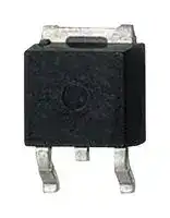


IKD08N65ET6ARMA1
IGBT, 15 A, 1.5 V, 47 W, 650 V, TO-252 (DPAK), 3 Pins
- Manufacturer: INFINEON
- Product type: Single IGBTs
- Available until stocks are exhausted Alternative available
- MSL: MSL 1 - Unlimited
- SVHC: No SVHC (27-Jun-2018)
- No. of Pins: 3Pins
- Product Range: TRENCHSTOP IGBT6
- Power Dissipation: 47W
- Transistor Mounting: Surface Mount
- DC Collector Current: 15A
- Power Dissipation Pd: 47W
- Transistor Case Style: TO-252 (DPAK)
- Operating Temperature Max: 175°C
- Continuous Collector Current: 15A
- Collector Emitter Voltage Max: 650V
- Automotive Qualification Standard: -
- Collector Emitter Voltage V(br)ceo: 650V
- Collector Emitter Saturation Voltage: 1.5V
- Collector Emitter Saturation Voltage Vce(on): 1.5V
| Delivery and price | |
|---|---|
| Units per pack | 1000 |
| Price | 0.763 € |
| Current stock | 1000+ |
| Lead time | 30 days |
## IKD08N65ET6

CE(sat) * Maximum junction temperature ¢ Short circuit withstand time 3us Trench and field-stop technology * very tight parameter * high ruggedness, temperature * low V CEsat and positive * Low gate charge Q G ¢ Pb-free lead plating; ROHS ¢ Very soft, fast recovery ¢« Complete product spectrum www.infineon.com/igbt Potential Applications: Drives ¢ GPD (general purpose drives)

**==> picture [96 x 231] intentionally omitted <==**

**----- Start of picture text -----**<br>
C<br>G<br>E<br>C<br>@ ,,<br>A a!<br>G<br>E a<br>**----- End of picture text -----**<br>


|**Type**|**_V_CE**|**_I_C**|**_V_CEsat** **_T_vj=25°C**|**_T_vjmax**|**Marking**|**Package**|
|---|---|---|---|---|---|---|
|IKD08N65ET6|650V|8A|1.5V|175°C|K08EET6|PG-TO252-3|


Datasheet www.infineon.com

2020-04-20

IKD08N65ET6

**==> picture [86 x 38] intentionally omitted <==**

## TRENCHSTOP™�IGBT6

## **Table�of�Contents**

Description   . . . . . . . . . . . . . . . . . . . . . . . . . . . . . . . . . . . . . . . . . . . . . . . . . . . . . . . . . . . . . . . . . . . . . . . . 1 Table of Contents   . . . . . . . . . . . . . . . . . . . . . . . . . . . . . . . . . . . . . . . . . . . . . . . . . . . . . . . . . . . . . . . . . . . 2 Maximum Ratings  . . . . . . . . . . . . . . . . . . . . . . . . . . . . . . . . . . . . . . . . . . . . . . . . . . . . . . . . . . . . . . . . . . . 3 Thermal Resistance   . . . . . . . . . . . . . . . . . . . . . . . . . . . . . . . . . . . . . . . . . . . . . . . . . . . . . . . . . . . . . . . . . 3 Electrical Characteristics  . . . . . . . . . . . . . . . . . . . . . . . . . . . . . . . . . . . . . . . . . . . . . . . . . . . . . . . . . . . . . . 4 Electrical Characteristics Diagrams   . . . . . . . . . . . . . . . . . . . . . . . . . . . . . . . . . . . . . . . . . . . . . . . . . . . . . 6 Package Drawing   . . . . . . . . . . . . . . . . . . . . . . . . . . . . . . . . . . . . . . . . . . . . . . . . . . . . . . . . . . . . . . . . . . .13 Testing Conditions   . . . . . . . . . . . . . . . . . . . . . . . . . . . . . . . . . . . . . . . . . . . . . . . . . . . . . . . . . . . . . . . . . .14 Revision History   . . . . . . . . . . . . . . . . . . . . . . . . . . . . . . . . . . . . . . . . . . . . . . . . . . . . . . . . . . . . . . . . . . . .15 Disclaimer  . . . . . . . . . . . . . . . . . . . . . . . . . . . . . . . . . . . . . . . . . . . . . . . . . . . . . . . . . . . . . . . . . . . . . . . . .16

2

V�2.3 2020-04-20

Datasheet

IKD08N65ET6

**==> picture [86 x 38] intentionally omitted <==**

## TRENCHSTOP™�IGBT6

## **Maximum�Ratings**

**For�optimum�lifetime�and�reliability,�Infineon�recommends�operating�conditions�that�do�not�exceed�80%�of�the�maximum�ratings�stated�in�this�datasheet.**

|**Parameter**|**Symbol**||**Value**|**Unit**|
|---|---|---|---|---|
|Collector-emittervoltage,_T_vj≥25°C|_V_CE||650|V|
|DCcollectorcurrent,limitedby_T_vjmax<br>_T_c=25°C<br>_T_c=100°C|_I_C||15.0<br>9.0|A|
|Pulsedcollectorcurrent,_t_plimitedby_T_vjmax|_I_Cpuls||25.0|A|
|Turnoffsafeoperatingarea_V_CE≤650V,_T_vj≤175°C|-||25.0|A|
|Diodeforwardcurrent,limitedby_T_vjmax<br>_T_c=25°C<br>_T_c=100°C|_I_F||15.0<br>10.0|A|
|Diodepulsedcurrent,_t_plimitedby_T_vjmax|_I_Fpuls||25.0|A|
|Gate-emitter voltage<br>TransientGate-emittervoltage(_t_p≤10µs,_D_<0.010)|_V_GE||±20<br>±30|V|
|Short circuit withstand time<br>_V_GE=15.0V,_V_CC≤360V<br>Allowed number of short circuits < 1000<br>Time between short circuits:≥1.0s<br>_T_vj=150°C|_t_SC||3|µs|
|Powerdissipation_T_c=25°C<br>Powerdissipation_T_c=100°C|_P_tot||47.0<br>23.0|W|
|Operating junction temperature|_T_vj|-40...+175||°C|
|Storage temperature|_T_stg|-55...+150||°C|
|Soldering temperature,<br>reflow soldering (MSL1 accordingto JEDEC J-STA-020)|||260|°C|


## **Thermal�Resistance**

|**ThermalResistance**|||||||
|---|---|---|---|---|---|---|
|**Parameter**|**Symbol **|**Conditions**||**Value**||**Unit**|
||||**min.**|**typ.**|**max.**||
|**RthCharacteristics**|||||||
|IGBT thermal resistance,<br>junction - case|_R_th(j-c)||-|-|3.20|K/W|
|Diode thermal resistance,<br>junction - case|_R_th(j-c)||-|-|4.60|K/W|
|Thermal resistance, min. footprint<br>junction - ambient|_R_th(j-a)||-|-|75|K/W|
|Thermal resistance, 6cm² Cu on<br>PCB<br>junction - ambient|_R_th(j-a)||-|-|50|K/W|


3

V�2.3 2020-04-20

Datasheet

IKD08N65ET6

**==> picture [86 x 38] intentionally omitted <==**

## TRENCHSTOP™�IGBT6

## **Electrical�Characteristic,�at�** _**T**_ **vj�=�25°C,�unless�otherwise�specified**

|**Parameter**|**Symbol **|**Conditions**||**Value**||**Unit**|
|---|---|---|---|---|---|---|
||||**min.**|**typ.**|**max.**||
|**StaticCharacteristic**|||||||
|Collector-emitter saturation voltage|_V_CEsat|_V_GE=15.0V,_I_C=5.0A<br>_T_vj=25°C<br>_T_vj=125°C<br>_T_vj=150°C|-<br>-<br>-|1.50<br>1.65<br>1.75|1.90<br>-<br>-|V|
|Diode forward voltage|_V_F|_V_GE=0V,_I_F=5.0A<br>_T_vj=25°C<br>_T_vj=125°C<br>_T_vj=150°C|-<br>-<br>-|1.28<br>1.21<br>1.15|1.75<br>-<br>-|V|
|Gate-emitter threshold voltage|_V_GE(th)|_I_C=0.12mA,_V_CE=_V_GE|4.8|5.6|6.4|V|
|Zero gate voltage collector current|_I_CES|_V_CE=650V,_V_GE=0V<br>_T_vj=25°C<br>_T_vj=150°C|-<br>-|-<br>240|30<br>-|µA|
|Gate-emitter leakage current|_I_GES|_V_CE=0V,_V_GE=20V|-|-|100|nA|
|Transconductance|_g_fs|_V_CE=20V,_I_C=5.0A|-|5.5|-|S|


## **Electrical�Characteristic,�at�** _**T**_ **vj�=�25°C,�unless�otherwise�specified**

|**Parameter**|**Symbol **|**Conditions**||**Value**||**Unit**|
|---|---|---|---|---|---|---|
||||**min.**|**typ.**|**max.**||
|**DynamicCharacteristic**|||||||
|Input capacitance|_C_ies|_V_CE=25V,_V_GE=0V<br>_f_=1000kHz|-|480|-|pF|
|Output capacitance|_C_oes||-|29|-||
|Reverse transfer capacitance|_C_res||-|8|-||
|Gate charge|_Q_G|_V_CC=520V,_I_C=5.0A,<br>_V_GE=15V|-|17.0|-|nC|
|Short circuit collector current<br>Max. 1000 short circuits<br>Time between short circuits:≥1.0s|_I_C(SC)|_V_GE=15.0V,_V_CC≤360V,<br>_t_SC≤3µs<br>_T_vj=150°C|-|50|-|A|


## **Switching�Characteristic,�Inductive�Load**

|**Parameter**|**Symbol **|**Conditions**||**Value**||**Unit**|
|---|---|---|---|---|---|---|
||||**min.**|**typ.**|**max.**||
|**IGBTCharacteristic,at****_T_vj=25°C**|||||||
|Turn-on delaytime|_t_d(on)|_T_vj=25°C,<br>_V_CC=400V,_I_C=5.0A,<br>_V_GE=0.0/15.0V,<br>_R_G(on)=47.0Ω,_R_G(off)=47.0Ω,<br>_L_σ=30nH,_C_σ=150pF<br>_L_σ,_C_σfromFig.E<br>Energy losses include “tail” and<br>diode reverse recovery.|-|20|-|ns|
|Rise time|_t_r||-|12|-|ns|
|Turn-off delaytime|_t_d(off)||-|59|-|ns|
|Fall time|_t_f||-|53|-|ns|
|Turn-on energy|_E_on||-|0.11|-|mJ|
|Turn-off energy|_E_off||-|0.04|-|mJ|
|Total switchingenergy|_E_ts||-|0.15|-|mJ|


V�2.3 2020-04-20

Datasheet

4

IKD08N65ET6

**==> picture [86 x 38] intentionally omitted <==**

## TRENCHSTOP™�IGBT6

**Diode�Characteristic,�at�** _**T**_ **vj�=�25°C**

|**DiodeCharacteristic,at****_T_vj=25°C**|||||||
|---|---|---|---|---|---|---|
|Diode reverse recoverytime|_t_rr|_T_vj=25°C,<br>_V_R=400V,<br>_I_F=5.0A,<br>_di_F_/dt_=400A/µs|-|43|-|ns|
|Diode reverse recoverycharge|_Q_rr||-|0.15|-|µC|
|Diodepeak reverse recoverycurrent|_I_rrm||-|4.9|-|A|
|Diode peak rate of fall of reverse<br>recoverycurrentduring_t_b|_di_rr_/dt_||-|-530|-|A/µs|


## **Switching�Characteristic,�Inductive�Load**

|**Parameter**|**Symbol **|**Conditions**||**Value**||**Unit**|
|---|---|---|---|---|---|---|
||||**min.**|**typ.**|**max.**||
|**IGBTCharacteristic,at****_T_vj=150°C**|||||||
|Turn-on delaytime|_t_d(on)|_T_vj=150°C,<br>_V_CC=400V,_I_C=5.0A,<br>_V_GE=0.0/15.0V,<br>_R_G(on)=47.0Ω,_R_G(off)=47.0Ω,<br>_L_σ=30nH,_C_σ=150pF<br>_L_σ,_C_σfromFig.E<br>Energy losses include “tail” and<br>diode reverse recovery.|-|18|-|ns|
|Rise time|_t_r||-|12|-|ns|
|Turn-off delaytime|_t_d(off)||-|69|-|ns|
|Fall time|_t_f||-|78|-|ns|
|Turn-on energy|_E_on||-|0.14|-|mJ|
|Turn-off energy|_E_off||-|0.07|-|mJ|
|Total switchingenergy|_E_ts||-|0.21|-|mJ|


**Diode�Characteristic,�at�** _**T**_ **vj�=�150°C**

|Diode reverse recoverytime|_t_rr|_T_vj=150°C,<br>_V_R=400V,<br>_I_F=5.0A,<br>_di_F_/dt_=400A/µs|-|65|-|ns|
|---|---|---|---|---|---|---|
|Diode reverse recoverycharge|_Q_rr||-|0.32|-|µC|
|Diodepeak reverse recoverycurrent|_I_rrm||-|7.2|-|A|
|Diode peak rate of fall of reverse<br>recoverycurrentduring_t_b|_di_rr_/dt_||-|-340|-|A/µs|


V�2.3 2020-04-20

Datasheet

5

IKD08N65ET6

**==> picture [474 x 322] intentionally omitted <==**

**----- Start of picture text -----**<br>
50<br>Ar<br>40<br>10<br>= BBAMIEiimUITati _<br>SAH Se<br>- ey tp = 1µs Zz<br>Wwef eHPiPi Ps2 30<br>S| LUI TE Pg<br>|a 1 LLUIME| | = 20<br>im CAM EIN i<br>fe) P-—t Ett —FFHt<br>oO ee ee ><br>> ee<br>Pt TTEETTT<br>ee| 10<br>0.1 0<br>1 10 100 1000 25 50 75 100 125 150 175<br>V CE , COLLECTOR-EMITTER VOLTAGE [V] T C , CASE TEMPERATURE [°C]<br>Figure 1. Forward bias safe operating area Figure 2. Power dissipation as a function of case<br>( D =0, T C =25°C, T vj 175°C; V GE=15V. temperature<br>Recommended use at V GE ≥ 15V) ( T vj ≤ 175°C)<br>I C P tot<br>**----- End of picture text -----**<br>


**==> picture [233 x 322] intentionally omitted <==**

**----- Start of picture text -----**<br>
18<br>15<br>NO<br>12<br>9<br>a \<br>: \<br>PLN<br>6<br>3<br>0<br>25 FTI 50 75 100 125 [LA] 150 | 175<br>T C , CASE TEMPERATURE [°C]<br>Figure 3. Collector current as a function of case<br>temperature<br>( V GE ≥ 15V, T vj ≤ 175°C)<br>I C<br>**----- End of picture text -----**<br>


**==> picture [231 x 285] intentionally omitted <==**

**----- Start of picture text -----**<br>
25<br>20<br>18V Ld<br>ET 15 VGE=20V Ay<br>15V<br>a 12V WA<br>e | ly<br>10 10V<br>la Hy<br>| 8V CHW<br>7V<br>5 6V<br>J N<br>0<br>0.0 0.5 1.0 Naa 1.5 2.0 2.5 3.0 3.5 4.0 n 4.5 5.0<br>V CE , COLLECTOR-EMITTER VOLTAGE [V]<br>I C<br>**----- End of picture text -----**<br>


Figure 4. Typical ( _T_ vj=25°C)

6

Datasheet

2020-04-20

IKD08N65ET6

**==> picture [490 x 285] intentionally omitted <==**

**----- Start of picture text -----**<br>
25 25<br>Tvj = 25°C<br>Tvj = 150°C<br>20 I 20 = a= /<br>VGE=20V<br>18V ea]7<br>15V<br>a)go5 15 12V a T TeeeW / |:ioa) 15 /<br>S| 10V OTT ls<br>Fe 8V 7 Fe<br>G 10 AG 10<br>a<br>7V _!<br>_! Nf J 7 4<br>6V<br>8 QW 8<br>. Wi .<br>5 5<br>Wes tN ft i,<br>yx x<br>0 es SN| Ze 0 —uw<br>0.0 0.5 1.0 1.5 2.0 2.5 3.0 3.5 4.0 4.5 5.0 5 6 7 8 9 10 11 12 13<br>V CE , COLLECTOR-EMITTER VOLTAGE [V] V GE , GATE-EMITTER VOLTAGE [V]<br>I C I C<br>**----- End of picture text -----**<br>


Figure 5. Typical ( _T_ vj=150°C)

Figure 6. Typical ( _V_ CE=50V)

**==> picture [471 x 286] intentionally omitted <==**

**----- Start of picture text -----**<br>
2.6<br>IC = 2.5A<br>IC = 5A<br>IC = 10A<br>100<br>Y5 7 a aa esee ee eee<br>-< 2.2 cad eeee<br>or eae “ ory a<br>E Pee £ a<br>= 1.8 O<br>uu -—“| =<br>(oe) -_” Ee 10 ke<br>S ot" = ee<br>1m _— _ a<br>= -— a es<br>1.4<br>fe ee<br>td(off)<br>tf<br>td(on)<br>tr<br>1.0 1<br>0 25 50 75 100 125 150 175 2 4 6 8 10<br>T vj , JUNCTION TEMPERATURE [°C] I C , COLLECTOR CURRENT [A]<br>t<br>CEsat<br>V<br>**----- End of picture text -----**<br>


Figure 8.

Figure 7. Typical collector-emitter saturation voltage as Figure 8. Typical switching times as a a function of junction temperature collector current ( _V_ GE=15V) (inductive load, _T_ vj =150°C, _V_ CE=400V, _V_ GE =0/15V, _r_ G=47 Ω , Dynamic test Figure E)

Datasheet

7

2020-04-20

IKD08N65ET6

**==> picture [474 x 593] intentionally omitted <==**

**----- Start of picture text -----**<br>
100<br>100 {a a _ eea a ieee<br>a S S<br>2 ee SS SSe Sd Ure eee es<br>c e<br>n EE SST eB<br>OQ betrrrereeee ee ee eee ee<br>2 frPrrrrprpryy2ey) eg {|Eft] || fF| fFft 7]<br>=r =r<br>O9 fofoa deere] Og oe<br>10<br>10<br>”a<br>eeaee ee ee ee ee ee ee es ee<br>ee eee ey ee ee<br>td(off) td(off)<br>tf tf<br>td(on) td(on)<br>tr tr<br>1 1<br>10 20 30 40 50 60 70 80 90 100 25 50 75 100 125 150 175<br>r G , GATE RESISTOR [ Ω ] T vj , JUNCTION TEMPERATURE [°C]<br>Figure 9. Typical switching times as a function of gate Figure 10. Typical switching times as a function of<br>resistor junction temperature<br>(inductive load, T vj =150°C, V CE=400V, (inductive load, V CE =400V, V GE=0/15V,<br>V GE =0/15V, I C =5.0A,Dynamic test circuit in I C =5A, r G=47 ,Dynamic test circuit in Figure<br>Figure E) E)<br>6 0.4<br>typ. Eoff<br>_ Eon /<br>Ets<br>al = Y<br>w<br>g<br>5 5 otE 0.3 4“<br>e) (ep) Y<br>> Ww 7?<br>(a) ep) a<br>a ie) ?<br>o aae) wo7 77<br>o 0 a 7<br>4 0.2<br>: i 7 a7<br>” i a“ -<br>wi ) Fa 7<br>- Zz “ -<br>S __ a -<br>ai = ‘ “<br>3 s 0.1 va |<br>2 0.0<br>25 50 75 100 125 150 175 2 3 4 5 6 7 8 9 10<br>T vj , JUNCTION TEMPERATURE [°C] I C , COLLECTOR CURRENT [A]<br>t t<br>E<br>GE(th)<br>V<br>**----- End of picture text -----**<br>


Figure 11. Gate-emitter of junction ( _I_ C=0.12mA)

Figure 12.

**==> picture [151 x 29] intentionally omitted <==**

**----- Start of picture text -----**<br>
(inductive load, T vj =150°C, V CE=400V,<br>V GE =0/15V, r G=47 Ω ,Dynamic test<br>Figure E)<br>**----- End of picture text -----**<br>


8

Datasheet

2020-04-20

IKD08N65ET6

**==> picture [490 x 642] intentionally omitted <==**

**----- Start of picture text -----**<br>
0.30 0.25<br>Eoff Eoff<br>Eon Eon<br>Ets Ets<br>= | Ea n<br>— - [oe] _ 0.20 EJ ] | | i<br>;<br>Lu - no “7<br>op)o 0.20 =- Wwop) -"_"<br>O 2 o ue<br>na -Poa | aO 0.15 _ - : | 7<br>-<br>a - 19) _-<br>Ww - w _|-<br>Zz = Ww -_-—<br>nT - - nTZz<br>19)oOZz - - oOZz 0.10 aaa<br>OO 0.10<br>S- EC __<br>° 0.05 an<br>0.00 0.00<br>10 20 30 40 50 60 70 80 90 100 25 50 75 100 125 150 175<br>r G , GATE RESISTOR [ Ω ] T vj , JUNCTION TEMPERATURE [°C]<br>Figure 13. Typical switching energy losses as a Figure 14. Typical switching energy losses as a<br>function of gate resistor function of junction temperature<br>(inductive load, T vj =150°C, V CE=400V, (inductive load, V CE =400V, V GE=0/15V,<br>V GE =0/15V, I C =5A, Dynamic test circuit in I C =5A, r G=47 ,Dynamic test circuit in Figure<br>Figure E) E)<br>0.3 16<br>Eoff —_— V CC = 130V<br>EEonts oe, 14 —- V CC =520V /<br>on<br>y¢<br>12<br>?<br>ty) 0.2 ae uw© /<br>10<br>oOa ”Fa 7 <a /<br>y a ><br>ow> 7 7 7 oOLi /<br>Ww , 7 EF 8 cr<br>oD a oo =<br>Zz= vv a 7 buMI 6 l<br>oO 0.1 <x /<br>5 laa 4<br>2<br>0.0 0<br>200 250 300 350 400 450 500 0 4 8 12 16 20<br>V CE , COLLECTOR-EMITTER VOLTAGE [V] Q G , GATE CHARGE [nC]<br>E E<br>GE<br>V<br>E<br>**----- End of picture text -----**<br>


**==> picture [41 x 9] intentionally omitted <==**

**----- Start of picture text -----**<br>
Figure 15.<br>**----- End of picture text -----**<br>


Figure 16. Typical ( _I_ C=5A)

**==> picture [154 x 29] intentionally omitted <==**

**----- Start of picture text -----**<br>
(inductive load, T vj =150°C, V GE=0/15V,<br>I C =5A, r G=47 ,Dynamic test circuit in<br>E)<br>**----- End of picture text -----**<br>


9

Datasheet

2020-04-20

IKD08N65ET6

**==> picture [469 x 643] intentionally omitted <==**

**----- Start of picture text -----**<br>
1000<br>SSS] HT<br>a ST PUI EIMATTIETTT<br>OSS 1 MNO<br>D = 0.5<br>\ xt RE ay, Sl WN TT TTT<br>100 A ee eee z am ESO A 0.2 a<br>- fv a ae shed,<br>ee a7 ey<br>0.1<br>SS i SE<br>a OY AN<br>0.1<br>FE a pt] 0.05<br>0.02<br>a eses nS afna<br>0.01<br>a. ~ F a<br>O me Z PLANITIA TTT<br>10<br>single pulse<br>aa ss es © 0.01 A(ee|oo ot CA eeeRe ||<br>a | | | |<br>Cies<br>a Coes aa ee ee ae ai ei ii GHGee |<br>Cres i: 1 2 3 4 5 6<br>ri[K/W]: 0.02726 0.42979 2.34397 0.36299 0.03488 1.1E-3<br>τ i[s]: 2.0E-5 1.8E-4 8.3E-4 4.5E-3 0.1233 4.273<br>1 mr ] tt 0.001 DTA M ———|<br>0 5 10 15 20 25 30 1E-6 1E-5 1E-4 0.001 0.01 0.1 1<br>V CE , COLLECTOR-EMITTER VOLTAGE [V] t p , PULSE WIDTH [s]<br>Figure 17. Typical capacitance as a function of Figure 18. IGBT transient thermal impedance<br>collector-emitter voltage ( D = t p/T)<br>( V GE =0V, f=1MHz)<br>90<br>Suit asi ease a ESR ES —<br>PTT TE CI TTT ate tert Tvj = 25°C, IF = 5Avj = 25°C, IF = 5A = 25°C, IF = 5AF = 5A = 5A<br>Tvj = 150°C, IF = 5Avj = 150°C, IF = 5A = 150°C, IF = 5AF = 5A = 5A<br>— eee<br>= TTT a<br>z TS At om [om ft —<br>YAN A<br>1<br>S< HEESSSP,ese D = 0.5 | — 70 ~ ~N<br>oO Pet A 0.2 re Ww<br>2 A ASA ICOM S ~. ~<br>0.1<br>SPyan a a<br>0.1 0.05<br>ow Co —- A—  — oO 50<br>Ww ew a... 0.02 | Ww<br>-= cmSetA Aa TS SECUM CT Th owWwWWwW pe<br>0.01<br>F2 HAa a HoH| WW Pee —=>—___|<br>single pulse<br>feBTC 0.01 SSTA TT TntmTy 1 sn |AIM LI)2 || ia 30<br>a a |<br>- BD) EG - yt  me ‘| Pf fT<br>wall i: ees 1 2 3 CiSAIRi_Co=felRe 4 5 6 |<br>ri[K/W]: 0.0475 0.4473 3.4385 0.624 0.054 1.5E-3<br>τ i[s]: 1.8E-5 1.3E-4 6.2E-4 3.5E-3 0.09017 3.99361<br>0.001 /| a 10 P| ff<br>1E-7 1E-6 1E-5 1E-4 0.001 0.01 0.1 1 300 400 500 600<br>t p ,PULSE WIDTH [s] di F /dt , DIODE CURRENT SLOPE [A/us]<br>C<br>c)th(j-<br>Z<br>t rr<br>c)th(j-<br>Z<br>**----- End of picture text -----**<br>


**==> picture [234 x 285] intentionally omitted <==**

**----- Start of picture text -----**<br>
90<br>—<br>Tvj = 25°C, IF = 5Avj = 25°C, IF = 5A = 25°C, IF = 5AF = 5A = 5A<br>Tvj = 150°C, IF = 5Avj = 150°C, IF = 5A = 150°C, IF = 5AF = 5A = 5A<br>a<br>—<br>70 ~<br>— ~N<br>Ww<br>S ~. ~<br>oO 50<br>Ww<br>owWwWWwW pe<br>WW Pee —=>—___|<br>ia 30 Pf fT<br>10 P| ff<br>300 400 500 600 700<br>di F /dt , DIODE CURRENT SLOPE [A/us]<br>t rr<br>**----- End of picture text -----**<br>


Figure 19. Diode function ( _D_ = _t_ p/T)

Figure 20.

( _V_ R=400V)

10

Datasheet

2020-04-20

IKD08N65ET6

**==> picture [475 x 303] intentionally omitted <==**

**----- Start of picture text -----**<br>
0.40 10<br>Tvj = 25°C, IF = 5A Tvj = 25°C, IF = 5A<br>Tvj = 150°C, IF = 5A Tvj = 150°C, IF = 5A<br>9<br>= 0.35 _— -<br>3 _ Lo<br>Lu Zz -<br>0 WW 8 LS<br>: SS ee : ~<br>0.30<br>i z a<br>rs) a) a<br>7<br>z = Z<br>WW uw 7<br>0.25<br>ia°2 0.20 oD8w 6 - eS—<br>Ww i 5 a<br>°<br>ci 0.15 —$—$——————s~* 2 ea<br>4<br>0.10 3<br>300 400 500 600 700 300 400 500 600 700<br>di F /dt , DIODE CURRENT SLOPE [A/us] di F /dt , DIODE CURRENT SLOPE [A/us]<br>Figure 21. Typical reverse recovery charge as a Figure 22. Typical reverse recovery current as a<br>Q rr I rr<br>**----- End of picture text -----**<br>


**==> picture [43 x 9] intentionally omitted <==**

**----- Start of picture text -----**<br>
( V R=400V)<br>**----- End of picture text -----**<br>


**==> picture [43 x 9] intentionally omitted <==**

**----- Start of picture text -----**<br>
( V R=400V)<br>**----- End of picture text -----**<br>


**==> picture [473 x 285] intentionally omitted <==**

**----- Start of picture text -----**<br>
-200 | 25<br>Tvj = 25°C, IF = 5A Tvj = 25°C<br>Tvj = 150°C, IF = 5A Tvj = 150°C<br>Sa = /<br>-300 | /<br>~~ 20<br>cya — [\/<br><, 7s RS —- =<<br>E -400 -<br>15<br>ia— rda<br>2fo) 3<br>Oo -500<br>a = 10 y<br>g2 -600 —_——_— a 5re<br>5<br>-700<br>7<br>Pf fo fl | /]<br>7<br>7<br>-800 0<br>300 400 500 600 700 0.5 1.0 1.5 2.0 2.5<br>di F /dt , DIODE CURRENT SLOPE [A/us] V F , FORWARD VOLTAGE [V]<br>I rr<br>/dt I F<br>rr<br>dI<br>**----- End of picture text -----**<br>


Figure 23.

Figure 24.

( _V_ R=400V)

11

Datasheet

2020-04-20

IKD08N65ET6

**==> picture [233 x 286] intentionally omitted <==**

**----- Start of picture text -----**<br>
1.8<br>1.6<br>eeLu ee<br>Kk2a 1.4<br>I<br>><br>gto<br>SsQgfeo 1.2 ~~ ~<br>oO ~<br>odiooeee<br>1.0<br>IF = 2.5A<br>IF = 5A<br>IF = 10A<br>F |y|e<br>0.8<br>25 50 75 100 125 150 175<br>T vj , JUNCTION TEMPERATURE [°C]<br>F<br>V<br>**----- End of picture text -----**<br>


Figure 25.

12

Datasheet

2020-04-20

IKD08N65ET6

**==> picture [86 x 38] intentionally omitted <==**

## TRENCHSTOP™�IGBT6

## Package Drawing PG-TO252-3

**==> picture [391 x 283] intentionally omitted <==**

**==> picture [140 x 55] intentionally omitted <==**

**==> picture [129 x 40] intentionally omitted <==**

**==> picture [158 x 167] intentionally omitted <==**

**----- Start of picture text -----**<br>
MILLIMETERS<br>DIM<br>MIN MAX<br>A 2.16 2.41<br>A1 0.00 0.15<br>b 0.64 0.89<br>b2 0.65 1.15<br>b3 4,95 5.50<br>c 0.46 0.61<br>c2 0.40 0.98<br>D 5.97 6.22<br>D1 5.02 5.84<br>E 6.35 6.73<br>E1 4.32 5.21<br>e 2.29 (BSC)<br>e1 4.57 (BSC)<br>N 3<br>H 9.40 10.48<br>L 1.18 1.78<br>L3 0.89 1.27<br>L4 0.51 1.02<br>**----- End of picture text -----**<br>


**==> picture [83 x 175] intentionally omitted <==**

**----- Start of picture text -----**<br>
DOCUMENT NO.<br>Z8B00003328<br>SCALE 0<br>2.5<br>0 2.5<br>5mm<br>EUROPEAN PROJECTION<br>ISSUE DATE<br>05-02-2016<br>REVISION<br>06<br>**----- End of picture text -----**<br>


13

V�2.3 2020-04-20

Datasheet

IKD08N65ET6

**==> picture [86 x 38] intentionally omitted <==**

## TRENCHSTOP™�IGBT6

## **Testing Conditions**

**==> picture [252 x 588] intentionally omitted <==**

**----- Start of picture text -----**<br>
V GE (t)<br>90%  V GE<br>10%  V GE t<br>I C (t)<br>90%  I C 90%  I C<br>10%  I C 10%  I C<br>t<br>V CE (t)<br>t<br>t d(off) t f t d(on) t r<br>Figure A.<br>V GE (t)<br>90%  V GE<br>10%  V GE<br>t<br>I C (t)<br>2%  I C t<br>V CE (t)<br>t 2 t 4<br>E off  [=] V CE x I C x d t E on  [=] V CE x I C x d t<br>t 1 t 3 2%  V CE<br>t<br>t 1 t 2 t 3 t 4<br>Figure B.<br>**----- End of picture text -----**<br>


**==> picture [153 x 99] intentionally omitted <==**

**----- Start of picture text -----**<br>
I,V<br>dI F /dt Qt rrrr== Qt aa++ tQ b b<br>a b<br>Q a Q b<br>dI<br>**----- End of picture text -----**<br>


Figure C. **Definition of diode switching characteristics**

**==> picture [7 x 7] intentionally omitted <==**

**----- Start of picture text -----**<br>
t<br>**----- End of picture text -----**<br>


**==> picture [169 x 63] intentionally omitted <==**

Figure D.

**==> picture [7 x 4] intentionally omitted <==**

**----- Start of picture text -----**<br>
CC<br>**----- End of picture text -----**<br>


Figure E. **Dynamic test circuit** Parasitic inductance Ls, parasitic capacitor Cs, relief capacitor C ,r (only for ZVT switching)

14

V�2.3 2020-04-20

Datasheet

IKD08N65ET6

**==> picture [86 x 38] intentionally omitted <==**

## TRENCHSTOP™�IGBT6

## **Revision�History**

IKD08N65ET6

## **Revision:�2020-04-20,�Rev.�2.3**

## Previous Revision

|Revision|Date|Subjects(major changes since last revision)|
|---|---|---|
|1.2|2020-03-16|PreliminaryData sheet|
|2.3|2020-04-20|Final|


15

V�2.3 2020-04-20

Datasheet

## **Trademarks**

## party.

## **Warnings**
Updated at June 9, 2026
Infineon Technologies is a globally recognized leader in semiconductor solutions, renowned for driving innovation in power management, energy efficiency, and modern mobility. With a strong legacy of engineering excellence, the company provides highly reliable components designed to meet the rigorous demands of industrial, automotive, and advanced commercial applications. The core of our Infineon portfolio is centered on their industry-leading discrete semiconductors. We offer an extensive selection of single and dual MOSFETs, alongside a robust range of single IGBTs and advanced IGBT modules. These flagship power transistors are essential for high-efficiency power conversion and motor control, providing engineers with superior thermal performance and minimized switching losses. Beyond advanced field-effect transistors, the selection includes a comprehensive array of diodes and rectifiers, heavily featuring Schottky diodes, as well as fast-recovery and RF/PIN diodes. This power foundation is further supported by bipolar transistors, intelligent power modules, and thyristor SCR modules, delivering the critical building blocks required for complex power system designs. To support broader system integration, the portfolio also encompasses specialized solutions such as solid-state relays, AC/DC LED driver ICs, and Bluetooth communications modules. From high-power industrial rectifiers to wireless connectivity adapters, Infineon equips designers with the precision components needed to build efficient, scalable, and fully connected electronic systems.
About Novapart
Novapart is a B2B electronic component broker specialising in stock shortages and cost reduction. We source hard-to-find parts and identify compliant alternatives across a catalogue of 410,000+ components from 500+ manufacturers.
Learn more →Stock Shortage Specialist
When a component is unavailable, discontinued or has an unacceptable lead time, we tap into our network of vetted European and Asian distributors to source what you need — without compromising on quality or traceability.
Request a quote →Compliant Alternatives
We identify pin-to-pin, electrically equivalent substitutes that meet the same certifications (RoHS, AEC-Q100, REACH) as your original specification — validated against datasheets, not just part numbers. Often at a lower cost.
BOM Analysis service →