


IHFW40N65R5SXKSA1
IGBT, 650 V, 61 A, 108W, HSIP247, 1.5 Vsat
- Manufacturer: INFINEON
- Product type: Single IGBTs
- SVHC: No SVHC (25-Jun-2025)
- No. of Pins: 3Pins
- Product Range: TRENCHSTOP 5
- Power Dissipation: 108W
- Transistor Mounting: Through Hole
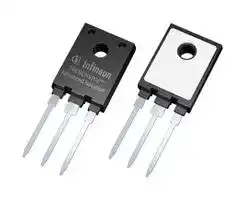
- Transistor Case Style: HSIP247
- Operating Temperature Max: 175°C
- Continuous Collector Current: 61A
- Collector Emitter Voltage Max: 650V
- Collector Emitter Saturation Voltage: 1.5V
| Delivery and price | |
|---|---|
| Units per pack | 1000 |
| Price | 2.47 € |
| Current stock | 10+ |
| Lead time | 30 days |
IHFW40N65R5S

## TRENCHSTOP[TM]

TM

**==> picture [471 x 16] intentionally omitted <==**

**----- Start of picture text -----**<br>
Reverse-Conducting IGBT in TRENCHSTOP _ TM 5 technology with monolithic<br>**----- End of picture text -----**<br>


**==> picture [480 x 203] intentionally omitted <==**

**----- Start of picture text -----**<br>
Features and Benefits: C<br>TRENCHSTOP [TM] 5 technology offering<br>* Best-in-Class efficiency in hard switching and resonant<br>topologies<br>¢ Plug and play replacement of previous generation IGBTs<br>G<br>* 650V breakdown voltage<br>E<br>* Low gate charge Q G<br>* Very soft, fast recovery antiparallel diode<br>¢ Maximum junction temperature 175°C<br>*2500V RMS _ electrical isolation, 50/60Hz, t=1min<br>* 100% tested isolated mounting surface<br>¢ Pb-free lead plating; ROHS compliant<br>*« Complete product spectrum and PSpice Models: Sf<br>http://www.infineon.com/igbt/<br>Potential Applications: =F 2<br>Fully isolated package TO-247<br>**----- End of picture text -----**<br>


|**Type**|**_V_CE**|**_I_C**|**_V_CEsat** **_T_vj=25°C**|**_T_vjmax**|**Marking**|**Package**|
|---|---|---|---|---|---|---|
|IHFW40N65R5S|650V|40A|1.5V|175°C|H40ER5S|PG-HSIP247-3-2|


Datasheet www.infineon.com

2020-07-10

IHFW40N65R5S

**==> picture [86 x 38] intentionally omitted <==**

## TRENCHSTOP[TM] �5�Advanced�Isolation

## **Table�of�Contents**

Description   . . . . . . . . . . . . . . . . . . . . . . . . . . . . . . . . . . . . . . . . . . . . . . . . . . . . . . . . . . . . . . . . . . . . . . . . 1 Table of Contents   . . . . . . . . . . . . . . . . . . . . . . . . . . . . . . . . . . . . . . . . . . . . . . . . . . . . . . . . . . . . . . . . . . . 2 Maximum Ratings  . . . . . . . . . . . . . . . . . . . . . . . . . . . . . . . . . . . . . . . . . . . . . . . . . . . . . . . . . . . . . . . . . . . 3 Thermal Resistance   . . . . . . . . . . . . . . . . . . . . . . . . . . . . . . . . . . . . . . . . . . . . . . . . . . . . . . . . . . . . . . . . . 3 Electrical Characteristics  . . . . . . . . . . . . . . . . . . . . . . . . . . . . . . . . . . . . . . . . . . . . . . . . . . . . . . . . . . . . . . 4 Electrical Characteristics Diagrams   . . . . . . . . . . . . . . . . . . . . . . . . . . . . . . . . . . . . . . . . . . . . . . . . . . . . . 6 Package Drawing   . . . . . . . . . . . . . . . . . . . . . . . . . . . . . . . . . . . . . . . . . . . . . . . . . . . . . . . . . . . . . . . . . . .13 Testing Conditions   . . . . . . . . . . . . . . . . . . . . . . . . . . . . . . . . . . . . . . . . . . . . . . . . . . . . . . . . . . . . . . . . . .14 Revision History   . . . . . . . . . . . . . . . . . . . . . . . . . . . . . . . . . . . . . . . . . . . . . . . . . . . . . . . . . . . . . . . . . . . .15 Disclaimer  . . . . . . . . . . . . . . . . . . . . . . . . . . . . . . . . . . . . . . . . . . . . . . . . . . . . . . . . . . . . . . . . . . . . . . . . .16

2

V�2.1 2020-07-10

Datasheet

IHFW40N65R5S

**==> picture [86 x 38] intentionally omitted <==**

## TRENCHSTOP[TM] �5�Advanced�Isolation

## **Maximum�Ratings**

**For�optimum�lifetime�and�reliability,�Infineon�recommends�operating�conditions�that�do�not�exceed�80%�of�the�maximum�ratings�stated�in�this�datasheet.**

|**Parameter**|**Symbol**||**Value**|**Unit**|
|---|---|---|---|---|
|Collector-emittervoltage,_T_vj≥25°C|_V_CE||650|V|
|DCcollectorcurrent,limitedby_T_vjmax<br>_T_h=25°C<br>_T_h=65°C<br>_T_h=65°C|_I_C||61.0<br>49.0<br>52.01)|A|
|Pulsedcollectorcurrent,_t_plimitedby_T_vjmax|_I_Cpuls||120.0|A|
|Turn off safe operating area<br>_V_CE≤650V,_T_vj≤175°C,_t_p=1µs|-||120.0|A|
|Diodeforwardcurrent,limitedby_T_vjmax<br>_T_h=25°C<br>_T_h=65°C|_I_F||44.0<br>40.0|A|
|Diodepulsedcurrent,_t_plimitedby_T_vjmax|_I_Fpuls||120.0|A|
|Gate-emitter voltage<br>TransientGate-emittervoltage(_t_p≤10µs,_D_<0.010)|_V_GE||±20<br>±30|V|
|Powerdissipation_T_h=25°C<br>Powerdissipation_T_h=65°C|_P_tot||108.0<br>79.0|W|
|Operating junction temperature|_T_vj|-40...+175||°C|
|Storage temperature|_T_stg|-55...+150||°C|
|Soldering temperature,<br>wave soldering1.6mm(0.063in.)from case for 10s|||260|°C|
|Mounting torque, M3 screw<br>Maximum of mounting processes: 3|_M_||0.6|Nm|
|IsolationvoltageRMS,_f_=50/60Hz,_t_=1min2)|_V_isol||2500|V|


## **Thermal�Resistance**

|**ThermalResistance**|||||||
|---|---|---|---|---|---|---|
|**Parameter**|**Symbol **|**Conditions**||**Value**||**Unit**|
||||**min.**|**typ.**|**max.**||
|**RthCharacteristics**|||||||
|IGBT thermal resistance,3)<br>junction - heatsink|_R_th(j-h)||-|1.19|1.39|K/W|
|Diode thermal resistance,3)<br>junction - heatsink|_R_th(j-h)||-|3.32|3.90|K/W|
|Thermal resistance<br>junction - ambient|_R_th(j-a)||-|-|65|K/W|


> 1) Equivalent current rating in TO-247-3 at Th = 65°C using reference insulation material: 152µm, 0.9 W/mK, standard polyimide based reinforced carrier insulator

> 2) For a proper handling and assembly of the advanced isolation device in the application refer to the note at the package drawing.

> 3) At force on body F = 500N, Ta = 25ºC

3

V�2.1 2020-07-10

Datasheet

IHFW40N65R5S

**==> picture [86 x 38] intentionally omitted <==**

## TRENCHSTOP[TM] �5�Advanced�Isolation

## **Electrical�Characteristic,�at�** _**T**_ **vj�=�25°C,�unless�otherwise�specified**

|**Parameter**|**Symbol **|**Conditions**||**Value**||**Unit**|
|---|---|---|---|---|---|---|
||||**min.**|**typ.**|**max.**||
|**StaticCharacteristic**|||||||
|Collector-emitter breakdown voltage|_V_(BR)CES|_V_GE=0V,_I_C=0.50mA|650|-|-|V|
|Collector-emitter saturation voltage|_V_CEsat|_V_GE=15.0V,_I_C=40.0A<br>_T_vj=25°C<br>_T_vj=175°C|-<br>-|1.50<br>1.85|2.00<br>-|V|
|Diode forward voltage|_V_F|_V_GE=0V,_I_F=40.0A<br>_T_vj=25°C<br>_T_vj=175°C|-<br>-|2.00<br>2.60|2.40<br>-|V|
|Gate-emitter threshold voltage|_V_GE(th)|_I_C=0.40mA,_V_CE=_V_GE|3.2|4.0|4.8|V|
|Zero gate voltage collector current|_I_CES|_V_CE=650V,_V_GE=0V<br>_T_vj=25°C<br>_T_vj=175°C|-<br>-|-<br>1000|40<br>-|µA|
|Gate-emitter leakage current|_I_GES|_V_CE=0V,_V_GE=20V|-|-|100|nA|
|Transconductance|_g_fs|_V_CE=20V,_I_C=40.0A|-|88.0|-|S|


## **Electrical�Characteristic,�at�** _**T**_ **vj�=�25°C,�unless�otherwise�specified**

|**Parameter**|**Symbol **|**Conditions**||**Value**||**Unit**|
|---|---|---|---|---|---|---|
||||**min.**|**typ.**|**max.**||
|**DynamicCharacteristic**|||||||
|Input capacitance|_C_ies|_V_CE=25V,_V_GE=0V<br>_f_=1000kHz|-|3428|-|pF|
|Output capacitance|_C_oes||-|34|-||
|Reverse transfer capacitance|_C_res||-|13|-||
|Gate charge|_Q_G|_V_CC=520V,_I_C=40.0A,<br>_V_GE=15V|-|142.0|-|nC|
|Internal emitter inductance<br>measured 5mm (0.197 in.) from<br>case|_L_E||-|13.0|-|nH|


## **Switching�Characteristic,�Inductive�Load**

|**Parameter**|**Symbol **|**Conditions**||**Value**||**Unit**|
|---|---|---|---|---|---|---|
||||**min.**|**typ.**|**max.**||
|**IGBTCharacteristic,at****_T_vj=25°C**|||||||
|Turn-on delaytime|_t_d(on)|_T_vj=25°C,<br>_V_CC=400V,_I_C=40.0A,<br>_V_GE=0.0/15.0V,<br>_R_G(on)=23.1Ω,_R_G(off)=23.1Ω,<br>_L_σ=40nH,_C_σ=50pF<br>_L_σ,_C_σfromFig.E<br>Energy losses include “tail” and<br>diode reverse recovery.|-|44|-|ns|
|Rise time|_t_r||-|38|-|ns|
|Turn-off delaytime|_t_d(off)||-|363|-|ns|
|Fall time|_t_f||-|27|-|ns|
|Turn-on energy|_E_on||-|1.52|-|mJ|
|Turn-off energy|_E_off||-|0.70|-|mJ|
|Total switchingenergy|_E_ts||-|2.22|-|mJ|


V�2.1 2020-07-10

Datasheet

4

IHFW40N65R5S

**==> picture [86 x 38] intentionally omitted <==**

## TRENCHSTOP[TM] �5�Advanced�Isolation

**Diode�Characteristic,�at�** _**T**_ **vj�=�25°C**

|**DiodeCharacteristic,at****_T_vj=25°C**|||||||
|---|---|---|---|---|---|---|
|Diode reverse recoverytime|_t_rr|_T_vj=25°C,<br>_V_R=400V,<br>_I_F=40.0A,<br>_di_F_/dt_=900A/µs|-|103|-|ns|
|Diode reverse recoverycharge|_Q_rr||-|2.48|-|µC|
|Diodepeak reverse recoverycurrent|_I_rrm||-|39.0|-|A|
|Diode peak rate of fall of reverse<br>recoverycurrentduring_t_b|_di_rr_/dt_||-|-1493|-|A/µs|


## **Switching�Characteristic,�Inductive�Load**

|**Parameter**|**Symbol **|**Conditions**||**Value**||**Unit**|
|---|---|---|---|---|---|---|
||||**min.**|**typ.**|**max.**||
|**IGBTCharacteristic,at****_T_vj=150°C**|||||||
|Turn-on delaytime|_t_d(on)|_T_vj=150°C,<br>_V_CC=400V,_I_C=40.0A,<br>_V_GE=0.0/15.0V,<br>_R_G(on)=23.1Ω,_R_G(off)=23.1Ω,<br>_L_σ=40nH,_C_σ=50pF<br>_L_σ,_C_σfromFig.E<br>Energy losses include “tail” and<br>diode reverse recovery.|-|40|-|ns|
|Rise time|_t_r||-|39|-|ns|
|Turn-off delaytime|_t_d(off)||-|424|-|ns|
|Fall time|_t_f||-|30|-|ns|
|Turn-on energy|_E_on||-|1.64|-|mJ|
|Turn-off energy|_E_off||-|0.86|-|mJ|
|Total switchingenergy|_E_ts||-|2.50|-|mJ|


**Diode�Characteristic,�at�** _**T**_ **vj�=�150°C**

|Diode reverse recoverytime|_t_rr|_T_vj=150°C,<br>_V_R=400V,<br>_I_F=40.0A,<br>_di_F_/dt_=900A/µs|-|149|-|ns|
|---|---|---|---|---|---|---|
|Diode reverse recoverycharge|_Q_rr||-|4.49|-|µC|
|Diodepeak reverse recoverycurrent|_I_rrm||-|51.0|-|A|
|Diode peak rate of fall of reverse<br>recoverycurrentduring_t_b|_di_rr_/dt_||-|-905|-|A/µs|


V�2.1 2020-07-10

Datasheet

5

IHFW40N65R5S

## TRENCHSTOP[TM]

**==> picture [489 x 642] intentionally omitted <==**

**----- Start of picture text -----**<br>
120<br>100<br>pp 100 RP Py fd<br>ee ee ee \<br>_ ee ee eIll<br>not for linear use<br>Se S a | z 80 \<br>10 LA M<br>a<br>UUM | UM 3 \<br>ad PT TTTin) 60<br>O Pt TT ETT o \<br>i<br>a<br>40<br>a 1 e) \<br>. — oe<br>aPeee etee= SaaaNG<br>Pt TT ETT 20 \<br>0.1 0<br>1 10 100 1000 25 50 75 100 125 150 175<br>V CE , COLLECTOR-EMITTER VOLTAGE [V] T h , HEATSINK TEMPERATURE [°C]<br>Figure 1. Forward bias safe operating area Figure 2. Power dissipation as a function of heatsink<br>( D =0, T h =25°C, T j 175°C, V GE =15V, t p ≤ 1µs) temperature<br>( T j ≤ 175°C)<br>70 120<br>VGE = 20V<br>60 Py] Pp td an jae<br>ae<br>100<br>17V<br>15V<br>oto ||/<br><x 50 <x|. Fej<br>80 13V<br>WW WW |<br>11V<br>e 40 \ ee<br>9V<br>: ; Sf pf<br>60<br>a a 8V Y Z| | 7<br>°O 30 ‘ ne)O a a(an<br>uw: Wwee 7V /oe|<br>40 6V<br>20<br>~ rN cee<br>\ |<br>20<br>10<br>\ ey Nee<br>aAne<br>0 0<br>25 50 75 100 125 150 175 0.0 0.5 1.0 1.5 2.0 2.5 3.0 3.5 4.0<br>T h , HEATSINK TEMPERATURE [°C] V CE , COLLECTOR-EMITTER VOLTAGE [V]<br>I C P tot<br>I C I C<br>**----- End of picture text -----**<br>


Figure 3. Collector current as **temperature** ( _V_ GE ≥ 15V, _T_ j ≤ 175°C)

Figure 4. Typical ( _T_ j=25°C)

6

Datasheet

2020-07-10

IHFW40N65R5S

## TRENCHSTOP[TM]

**==> picture [469 x 285] intentionally omitted <==**

**----- Start of picture text -----**<br>
120 120<br>Tvj = 25°C<br>Pe | /A ee ee Tvj = 150°C<br>VGE = 20V _f = |<br>100 er 100<br>17V |) | aes ee ee ee<br>15V Ml Z|)  |<br>80 13V 80<br>mm: “yfH 7— mm=} i | | fg<br>11V<br>; pf BL<br>9V<br>60 60<br>8V<br>ee<br>7V<br>: |/ eee ee ee ee<br>40 6V eS ee 40 eee eeee<br>5V<br>20 20<br>ae ee<br>0 0<br>0 1 2 3 4 5 2 3 4 5 6 7 8<br>V CE , COLLECTOR-EMITTER VOLTAGE [V] V GE , GATE-EMITTER VOLTAGE [V]<br>I C I C<br>**----- End of picture text -----**<br>


Figure 5. Typical ( _T_ j=150°C)

Figure 6. Typical ( _V_ CE=20V)

**==> picture [471 x 331] intentionally omitted <==**

**----- Start of picture text -----**<br>
3.0 IC = 20A [ _ td(off)<br>IC = 40A tf<br>I a ee ee<br>IC = 60A td(on)<br>= | a ee<br>S 2.5 I tr ee e eee<br>1000<br>3 ba ae<br>E e e<br>wa=) _ e eeeee ee<br>2.0 a a<br>Ee0 aa ~ QO7) I| ————_—~| | J |<br>100<br>Ee 1.5 — O ee<br>i<br>owOo© 1.0 Tf oOEFS| |EN [Sessa] [Tapeeeeee<br>Oo 10 poner | |<br>O [_<br>. a es<br>a ss<br>0.5 a es<br>a ee<br>Pe<br>0.0 1<br>25 50 75 100 125 150 175 0 10 20 30 40 50 60<br>T j , JUNCTION TEMPERATURE [°C] I C , COLLECTOR CURRENT [A]<br>Figure 7. Typical collector-emitter saturation voltage as Figure 8. Typical switching times as a function of<br>a function of junction temperature collector current<br>( V GE=15V) (ind. load, T j =150°C, V CE =400V, V GE=0/15V,<br>R G=23.1 , test circuit in Fig. E)<br>t<br>CE(sat)<br>V<br>**----- End of picture text -----**<br>


Datasheet

7

2020-07-10

IHFW40N65R5S

## TRENCHSTOP[TM]

**==> picture [474 x 677] intentionally omitted <==**

**----- Start of picture text -----**<br>
td(off) td(off)<br>1000 tf 1000 tf<br>1 E |t| ttd(on)r LLs} aaa aeeesee eeeeeeeeee eeee eeeeeeeee xe |tt ttd(on)r aaaeeee ee<br>SS a es es ee SS a<br>a e e ee ee ee ee a e s<br>ee ee a<br>~ ~-A Fite} fo fe}<br>cc<br>e<br>100 100<br>Ww felt Tet ity se LE | ft |<br>= eea a | uw a<br>= po eee eer cee ee = [_a<br>9 a cscl i 9 Pma mm me a ee fe e e<br>= a ee ee a ae ee ee e e<br>OS t u e tT | | | | | |} @ F e a<br>a<br>n n<br>10 ° 10<br>a ee<br>a<br>po aa ee<br>a ee ee ee a ee<br>| ot | | ft | ct ht es ee ee ee<br>1 1<br>0 10 20 30 40 50 60 70 80 90 25 50 75 100 125 150<br>R G , GATE RESISTOR [ Ω ] T j , JUNCTION TEMPERATURE [°C]<br>Figure 9. Typical switching times as a function of gate Figure 10. Typical switching times as a function of<br>resistor junction temperature<br>(ind. load, T j =150°C, V CE  =400V, V GE=0/15V, (ind. load, V CE =400V, V GE =0/15V, I C=40A,<br>I C =40A, test circuit in Fig. E) r G=23.1 , test circuit in Fig. E)<br>6 5.0<br>typ. Eoff<br>min. 4.5 Eon<br>max. Ets<br>5<br>Oo = 4.0 /<br>O ss 40 7p) ’<br>> 4 ae HM 3.5<br>fe)x= Spe se o 3.0 /<br>He *\ > J<br>x 3 _—~™_ ‘ or 2.5<br>oe- ~_. ~~NN Zzuw 77 7 7<br>: SWl 2 ~~. _ON E5 2.01.5 “vear7 ZO<br>s| 1 1.0<br>aaaea —_|<br>0.5 ><br>0 0.0<br>25 50 75 100 125 150 175 0 10 20 30 40 50 60<br>T j , JUNCTION TEMPERATURE [°C] I C , COLLECTOR CURRENT [A]<br>Figure 11. Gate-emitter threshold voltage as a function Figure 12. Typical switching energy losses as a<br>of junction junction temperature function of collector current<br>( I C=0.4mA)=0.4mA) (ind. load, T j =150°C, V CE =400V, V GE=0/15V,<br>t t<br>E<br>GE(th)<br>V<br>**----- End of picture text -----**<br>


Figure 11. Gate-emitter of junction junction ( _I_ C=0.4mA)=0.4mA)

_R_ G=23.1

8

Datasheet

2020-07-10

IHFW40N65R5S

## TRENCHSTOP[TM]

**==> picture [491 x 679] intentionally omitted <==**

**----- Start of picture text -----**<br>
5.0 3.0<br>Eoff Eoff<br>4.5 Eon Eon<br>Ets Ets<br>2.5<br>~~ 4.0 ~~<br>3.5<br>(0 52 (0<br>7)(op) va, 7)(op) 2.0<br>—! 3.0 —!<br>oO , oO<br>o~ Fa o~<br>WwW 2.5 WwW 1.5<br>Zz oa - Zz<br>Lu oe -_ Lu<br>2.0<br>_— an<br>1.0<br>SB | eT<br>1.5<br>an | 8<br>: am SE aaa<br>a i<br>1.0<br>Ed i 0.5 ee<br>0.5<br>0.0 0.0<br>0 10 20 30 40 50 60 70 80 90 25 50 75 100 125 150<br>R G , GATE RESISTOR [ Ω ] T j , JUNCTION TEMPERATURE [°C]<br>Figure 13. Typical switching energy losses as a Figure 14. Typical switching energy losses as a<br>function of gate resistor function of junction temperature<br>(ind. load, T j =150°C, V CE  =400V, V GE=0/15V, (indload, V CE =400V, V GE =0/15V, I C=40A,<br>I C =40A, test circuit in Fig. E) R G=23.1 , test circuit in Fig. E)<br>4.0 16 P|<br>Eoff V CC<br>Eon a —_—- V CC =520V= 130V<br>3.5 Ets > < 14 =<br>¢<br>a & 3.0 e e77 S 12 a e<br>io) Y<br>ieeenO ? 7 a< eee eee<br>O 2.5 ¢ 7 FE 10<br>4 ¢v 7 oO<br>Www 2.0 ¢ af” Ww= 8<br>i“7<br>e) :7 =<br>Z 1.5 4 i 6<br>= / / 7 LuEK oc<br>==4vv, 7 7 7 5~<br>1.0 4<br>0.5 2<br>0.0 0<br>200 300 400 500 600 0 20 40 60 80 100 120 140 160<br>V CE , COLLECTOR-EMITTER VOLTAGE [V] Q GE , GATE CHARGE [nC]<br>Figure 15. Typical switching energy losses as a Figure 16. Typical gate charge<br>function of collector emitter voltage ( I C=40A)<br>(ind. load, T j =150°C, V GE =0/15V, I C=40A,<br>E E<br>GE<br>V<br>E<br>**----- End of picture text -----**<br>


**==> picture [34 x 8] intentionally omitted <==**

**----- Start of picture text -----**<br>
R G=23.1<br>**----- End of picture text -----**<br>


9

Datasheet

2020-07-10

IHFW40N65R5S

TRENCHSTOP[TM]

**==> picture [478 x 676] intentionally omitted <==**

**----- Start of picture text -----**<br>
Cies<br>1E+4 F Coes ee 1<br>Cres<br>I a | tn Ill<br>D = 0.5<br>a 7) CH ae Sn<br>Ce 89? 0.2 NN<br>1000 pT | | | | OR7.<br>_ eeee ee eee MGT ee maT 0.1<br>ieeee ) 0.1 Ly Ce saa nT 0.05<br>a All<br>0.02<br>CA Sani aan 0.01<br>100 single pulse<br>7 ee ST UTTER RTIT GHIA<br>eesass 0.01 TT)eA<br>10 w ee | | -—7— Ul<br>SSS SS a i<br>es ee a a er ae 0<br>i: 1 2 3 4 5 6 7<br>ee ri[K/W]: P7UT 0.015257 EC 0.27071 CT 0.29854 0.24739 TTT 0.34111 ET 0.20394 ETT 0.017347 TT<br>τ i[s]: 2.6E-5 3.0E-4 2.6E-3 0.022827 0.287773 1.293832 18.69534<br>1 0.001<br>0 5 10 15 20 25 30 1E-6 1E-5 1E-4 0.001 0.01 0.1 1 10<br>V CE , COLLECTOR-EMITTER VOLTAGE [V] t p , PULSE WIDTH [s]<br>Figure 17. Typical capacitance as a function of Figure 18. IGBT transient thermal impedance as a<br>collector-emitter voltage function of pulse width<br>( V GE =0V, f=1MHz) ( D = t p/T)<br>PT TT TET 200 Ld<br>a<br>Tvj = 25°C, IF = 40Avj = 25°C, IF = 40A = 25°C, IF = 40AF = 40A = 40A<br>Tvj = 150°C, IF = 40Avj = 150°C, IF = 40A = 150°C, IF = 40AF = 40A = 40A<br>= SAST TT TE Saeaeeeent TTT 180 See - -_<br>2 1 D = 0.5 160 — ee ee<br>O UIE Il pt<br>Zz= peneeAeOfee 0.2 LOT|ottTO gccyWwWcyWwWWwW 140 tL<br>0.1<br>a Stiiases 26 Sn SH s<br>0.05<br>tl& AEE 7AN A | Pe~~~~ —<br>120<br>0.02<br>2 0.1 este 0.01 MALI & ae<br>Wwx OAth single pulse AEE = 100<br>- > oo III wd<br>bE= eee| ATT ee uwtH 80 Pf fff]<br>Z ET A cm tH<br>2 PIM AU IT ETT TTT T I 9 60 Pf fff]<br>UAE Ra<br>fe 0.01 A ' ° nn) o<br>ke°AHH | | | on i 40 Pf fff]<br>a<br>aeaeewlt_—n i: 1 2 3 tut wt 4 5 _—~$ 6 7 | 20 Pot of tp<br>ri[K/W]: 0.034177 2.3111 0.68651 0.28831 0.27698 0.28622 0.0169<br>τ i[s]: 1.8E-5 2.2E-4 1.5E-3 0.018085 0.20635 0.990087 18.58714<br>0.001 | 0 Pt fff<br>1E-7 1E-6 1E-5 1E-4 0.001 0.01 0.1 1 400 500 600 700 800 900<br>t p , PULSE WIDTH [s] di F /dt , DIODE CURRENT SLOPE [A/us]<br>Figure 19. Diode transient thermal impedance as a Figure 20. Typical reverse recovery time as a function<br>function of pulse width of diode current slope<br>( D = t p/T) ( V R=400V)<br>C<br>h)th(j-<br>Z<br>t rr<br>h)th(j-<br>Z<br>**----- End of picture text -----**<br>


**==> picture [235 x 285] intentionally omitted <==**

**----- Start of picture text -----**<br>
200 Ld<br>Tvj = 25°C, IF = 40Avj = 25°C, IF = 40A = 25°C, IF = 40AF = 40A = 40A<br>Tvj = 150°C, IF = 40Avj = 150°C, IF = 40A = 150°C, IF = 40AF = 40A = 40A<br>180 See - -_<br>160<br>— ee ee<br>pt<br>gccyWwWcyWwWWwW 140 tL<br>s<br>Pe~~~~ —<br>& 120 ae<br>100<br>=<br>wd<br>uwtH 80 Pf fff]<br>9 60 Pf fff]<br>o<br>40 Pf fff]<br>20<br>Pot of tp<br>0 Pt fff<br>400 500 600 700 800 900 1000<br>di F /dt , DIODE CURRENT SLOPE [A/us]<br>t rr<br>**----- End of picture text -----**<br>


10

Datasheet

2020-07-10

IHFW40N65R5S

## TRENCHSTOP[TM]

**==> picture [476 x 285] intentionally omitted <==**

**----- Start of picture text -----**<br>
6 60<br>Tvj = 25°C, IF = 40A Tvj = 25°C, IF = 40A<br>Tvj = 150°C, IF = 40A Tvj = 150°C, IF = 40A<br>= ee | = | /<br>2 5 | 50 | | ’<br>2Wwo L “7 vy | =a LY7 “e<br>4 40<br>$ - £ <<br>© oe ro)a) oo<br>ag ><br>im2 a a iT YO<br>Q 3 >fe) 30<br>or or<br>He2 2 > — |— | 2° 20 — |—<br>Ww - uw<br>oc<br>or i<br>1 10<br>0 0<br>400 500 600 700 800 900 1000 400 500 600 700 800 900 1000<br>di F /dt , DIODE CURRENT SLOPE [A/us] di F /dt , DIODE CURRENT SLOPE [A/us]<br>Q rr I rr<br>**----- End of picture text -----**<br>


Figure 21.

( _V_ R=400V)

Figure 22.

( _V_ R=400V)

**==> picture [469 x 285] intentionally omitted <==**

**----- Start of picture text -----**<br>
0 120<br>Tvj = 25°C, IF = 40A Tvj = 25°C<br>-200 Tvj = 150°C, IF = 40A Tvj = 150°C /<br>= /<br>100<br>zge] -400 ON ET<br>\ / /<br>ue ~“ > /<br>-600<br>e) ~ ' <x— / //<br>3 kK 80<br>im -800 Ww /<br>ue ~<br>uw ) /<br>-1000 60<br>\ x /<br>< -1200 <x /<br>wi =<br>Oo e)a 40<br>ow -1400 \ | Poff<br>|<br>-1600<br>20<br>Po ff<br>-1800<br>-2000 0<br>400 500 600 700 800 900 1000 0 1 2 3 4 5 6<br>di F /dt , DIODE CURRENT SLOPE [A/us] V F , FORWARD VOLTAGE [V]<br>I rr<br>I F<br>/dt<br>rr<br>dI<br>**----- End of picture text -----**<br>


Figure 23.

Figure 24.

( _V_ R=400V)

11

Datasheet

2020-07-10

IHFW40N65R5S

## TRENCHSTOP[TM]

**==> picture [233 x 286] intentionally omitted <==**

**----- Start of picture text -----**<br>
4.0<br>IF = 20A<br>IF = 40A<br>3.5 IF = 60A<br>3.0<br>Ww<br>iv)~¢ 2.5 —_—? -<br>a _<br>|<br>>Q 2.0 _—<br>ef<br>1.5<br>1.0<br>0.5<br>0.0<br>25 50 75 100 125 150 175<br>T j , JUNCTION TEMPERATURE [°C]<br>F<br>V<br>**----- End of picture text -----**<br>


Figure 25.

12

Datasheet

2020-07-10

IHFW40N65R5S

**==> picture [86 x 38] intentionally omitted <==**

## TRENCHSTOP[TM] �5�Advanced�Isolation

## **PG-HSIP247-3-2**

**==> picture [431 x 640] intentionally omitted <==**

**----- Start of picture text -----**<br>
MILLIMETERS MILLIMETERS<br>DIMENSIONS DIMENSIONS<br>MIN. MAX. MIN. MAX.<br>A    - 5.18 e 5.44<br>A1 4.70 4.90 E 15.70 15.90<br>A2 2.16 2.66 E1 13.68 13.88<br>DOCUMENT NO.<br>A3 0.20 0.28 E2 (6.00)<br>Z8B00195711<br>A4 1.30 1.50 E3 3.24 3.44<br>A5 0.31 0.51 E4 4.39 4.59 REVISION<br>A6 1.70 1.90 E5 (1.45) 01<br>A7 (0.25) E6 0.76 0.96<br>b 1.10 1.30 L 18.01 18.21 SCALE 3:1<br>b1 (2.88) L1 2.26 2.46 0 1 2 3 4 5 6 7 8mm<br>b2 (1.60) L2 1.50 1.70<br>b3    - 0.15 P 3.50 3.70<br>c 0.50 0.70 P1 5.70 5.90 EUROPEAN PROJECTION<br>D 22.70 22.90 Q 6.06 6.26<br>D1 16.96 17.16<br>D2 2.34 2.54<br>D3    - 0.30<br>ISSUE DATE<br>D4 4.35 4.55<br>28.06.2019<br>D5 19 70 19 90<br>**----- End of picture text -----**<br>


13

V�2.1 2020-07-10

Datasheet

IHFW40N65R5S

**==> picture [86 x 38] intentionally omitted <==**

## TRENCHSTOP[TM] �5�Advanced�Isolation

## **Testing Conditions**

**==> picture [252 x 588] intentionally omitted <==**

**----- Start of picture text -----**<br>
V GE (t)<br>90%  V GE<br>10%  V GE t<br>I C (t)<br>90%  I C 90%  I C<br>10%  I C 10%  I C<br>t<br>V CE (t)<br>t<br>t d(off) t f t d(on) t r<br>Figure A.<br>V GE (t)<br>90%  V GE<br>10%  V GE<br>t<br>I C (t)<br>2%  I C t<br>V CE (t)<br>t 2 t 4<br>E off  [=] V CE x I C x d t E on  [=] V CE x I C x d t<br>t 1 t 3 2%  V CE<br>t<br>t 1 t 2 t 3 t 4<br>Figure B.<br>**----- End of picture text -----**<br>


**==> picture [189 x 170] intentionally omitted <==**

**----- Start of picture text -----**<br>
I,V<br>dI F /dt Qt rrrr== Qt aa++ tQ b b<br>a b<br>Q a Q b<br>dI<br>Figure C.  Definition of diode switching<br>characteristics<br>**----- End of picture text -----**<br>


**==> picture [7 x 7] intentionally omitted <==**

**----- Start of picture text -----**<br>
t<br>**----- End of picture text -----**<br>


**==> picture [169 x 63] intentionally omitted <==**

Figure D.

**==> picture [7 x 4] intentionally omitted <==**

**----- Start of picture text -----**<br>
CC<br>**----- End of picture text -----**<br>


Figure E. **Dynamic test circuit** Parasitic inductance Ls, parasitic capacitor Cs, relief capacitor C ,r (only for ZVT switching)

14

V�2.1 2020-07-10

Datasheet

IHFW40N65R5S

**==> picture [86 x 38] intentionally omitted <==**

## TRENCHSTOP[TM] �5�Advanced�Isolation

## **Revision�History**

IHFW40N65R5S

## **Revision:�2020-07-10,�Rev.�2.1**

## Previous Revision

|Revision|Date|Subjects(major changes since last revision)|
|---|---|---|
|1.1|2020-05-07|PreliminaryData Sheet|
|2.1|2020-07-10|Final data sheet|


15

V�2.1 2020-07-10

Datasheet

## **Trademarks**

## party.

## **Warnings**
Updated at June 9, 2026
Infineon Technologies is a globally recognized leader in semiconductor solutions, renowned for driving innovation in power management, energy efficiency, and modern mobility. With a strong legacy of engineering excellence, the company provides highly reliable components designed to meet the rigorous demands of industrial, automotive, and advanced commercial applications. The core of our Infineon portfolio is centered on their industry-leading discrete semiconductors. We offer an extensive selection of single and dual MOSFETs, alongside a robust range of single IGBTs and advanced IGBT modules. These flagship power transistors are essential for high-efficiency power conversion and motor control, providing engineers with superior thermal performance and minimized switching losses. Beyond advanced field-effect transistors, the selection includes a comprehensive array of diodes and rectifiers, heavily featuring Schottky diodes, as well as fast-recovery and RF/PIN diodes. This power foundation is further supported by bipolar transistors, intelligent power modules, and thyristor SCR modules, delivering the critical building blocks required for complex power system designs. To support broader system integration, the portfolio also encompasses specialized solutions such as solid-state relays, AC/DC LED driver ICs, and Bluetooth communications modules. From high-power industrial rectifiers to wireless connectivity adapters, Infineon equips designers with the precision components needed to build efficient, scalable, and fully connected electronic systems.
About Novapart
Novapart is a B2B electronic component broker specialising in stock shortages and cost reduction. We source hard-to-find parts and identify compliant alternatives across a catalogue of 410,000+ components from 500+ manufacturers.
Learn more →Stock Shortage Specialist
When a component is unavailable, discontinued or has an unacceptable lead time, we tap into our network of vetted European and Asian distributors to source what you need — without compromising on quality or traceability.
Request a quote →Compliant Alternatives
We identify pin-to-pin, electrically equivalent substitutes that meet the same certifications (RoHS, AEC-Q100, REACH) as your original specification — validated against datasheets, not just part numbers. Often at a lower cost.
BOM Analysis service →