
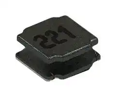


IFSC1616AHER6R8M01
Power Inductor (SMD), 6.8 µH, 1.7 A, Shielded, 1.8 A, IFSC1616AH-01 Series
- Manufacturer: VISHAY
- Product type: SMD Power Inductors
- SVHC: No SVHC (07-Nov-2024)
- Inductance: 6.8µH
- Product Width: 4mm
- Product Height: 1.8mm
- Product Length: 4mm
- DC Resistance Max: 0.118ohm
- RMS Current (Irms): 1.7A
- Saturation Current (Isat): 1.8A
| Delivery and price | |
|---|---|
| Units per pack | 3000 |
| Price | 0.101 € |
| Current stock | 1000+ |
| Lead time | 30 days |
Surface Mount Multilayer Ceramic Chip Capacitors (SMD MLCCs) **ESD, C0G Dielectric, 25 – 250 VDC (Commercial & Automotive Grade)**

## **Overview**

The KEMET electrostatic discharge (ESD) rated commercial and automotive grade surface mount capacitors in C0G dielectric are suited for a variety of applications where electrostatic discharge (ESD) events during assembly or operation could damage the capacitor or the circuit. These ESD rated capacitors provide the ability to design within a given ESD criteria per the human body model (HBM) AEC Q200–002 criteria. The KEMET automotive grade capacitors also meet the other demanding Automotive Electronics Council's AEC–Q200 qualification requirements.

The C0G dielectric features a 125°C maximum operating temperature and is considered “stable.” The Electronics Industries Alliance (EIA) characterizes C0G dielectric as a Class I material. Components of this classification are temperature compensating and are suited for resonant circuit applications, as well as those where Q and stability of capacitance characteristics are required. The C0G dielectric exhibits no change in capacitance with respect to time and voltage, and boasts a negligible change in capacitance compared to its value at 25°C. Capacitance change is limited to ±30 ppm/°C from −55°C to +125°C.

## **Benefits**

- AEC-Q200 automotive qualified

- ESD qualified per HBM - AEC Q200-002

- Available in package size EIA 0402, 0603, 0805, 1206

- DC Voltage ratings of 25 V, 50 V, 63 V, 100 V, 200 V and 250 V

- Capacitance range from 1 nF to 100 nF

- −55°C to +125°C operating temperature range

- Lead (Pb)-free, RoHS and REACH compliant

- Available capacitance tolerances of ±1%, ±2%, ±5%, ±10%, and ±20%

- No piezoelectric noise

- Extremely low ESR and ESL

- High thermal stability

- High ripple current capability

Click image above for interactive 3D content Click image above for interactive 3D content _Open PDF in Adobe Reader for full functionality_ Open PDF in Adobe Reader for full functionality

- Preferred capacitance solution at line frequencies and into the MHz range

- No capacitance changes with respect to applied DC voltage

- Negligible capacitance change with respect to temperature from −55°C to +125°C

- No capacitance decay with time

- Non-polar devices, minimizing installation concerns

- 100% pure matte tin-plated termination finish allowing for excellent solderability

- Flexible Termination option available

## **Applications**

Typical applications include: electrostatic discharge (ESD), integrated circuit (IC) protection, radio frequency (RF) filtering function, input and output automotive applications such as controllers, navigation systems, airbags and keyless systems.

**Built Into Tomorrow**

© KEMET Electronics Corporation • KEMET Tower • One East Broward Boulevard Fort Lauderdale, FL 33301 USA • 954-766-2800 • www.kemet.com

C1091_C0G_ESD • 9/15/2020 1

Surface Mount Multilayer Ceramic Chip Capacitors (SMD MLCCs) ESD, C0G Dielectric, 25 – 250 VDC (Commercial & Automotive Grade)

## **Ordering Information**

|**C**|**0603**|**C**|**103**|**J**|**3**|**G**|**E**|**C**|**AUTO**|
|---|---|---|---|---|---|---|---|---|---|
|Ceramic|Case Size<br>(L" x W")|Specifcation/<br>Series|<br>Capacitance<br>Code (pF)|Capacitance<br>Tolerance2|Rated Voltage<br>(VDC)|Dielectric|Failure Rate/<br>Design|Termination<br>Finish2|Packaging/<br>Grade<br>(C-Spec)|
||0402<br>0603<br>0805<br>1206|C = Standard<br>X = Flexible<br>Termination|Two<br>signifcant<br>digits and<br>number of<br>zeros|F = ±1%<br>G = ±2%<br>J = ±5%<br>K = ±10%<br>M = ±20%|3 = 25<br>5 = 50<br>M = 63<br>1 = 100<br>2 = 200<br>A = 250|G = C0G|E = ESD|C = 100%<br>Matte Sn|See<br>"Packaging<br>C-Spec<br>Ordering<br>Options<br>Table"|


_1 Additional capacitance tolerance offerings may be available. Contact KEMET for details._

_2 Additional capacitance tolerance offerings and termination finish options may be available. Contact KEMET for details.Benefits (cont'd)_

## **Table 1A – Capacitance Range/Selection Waterfall**

**==> picture [542 x 205] intentionally omitted <==**

**----- Start of picture text -----**<br>
Case Size/<br>C0402C C0603C C0805C C1206C<br>Series<br>Rated Voltage  25 50 63 100 25 50 63 100 200 25 50 63 100 200 250 25 50 63 100 200 250<br>Capacitance Cap Code (VDC)<br>Voltage Code 3 5 M 1 3 5 M 1 2 3 5 M 1 2 A 3 5 M 1 2 A<br>Cap Tolerance ESD Level per AEC–Q200<br>1.0 nF 102 4 kV 4 kV 4 kV 4 kV 6 kV 6 kV 6 kV 6 kV 6 kV 8 kV 8 kV 8 kV 8 kV 8 kV 8 kV 12 kV 12 kV 12 kV 12 kV 12 kV 12 kV<br>1.5 nF 152 6 kV 6 kV 8 kV 8 kV 8 kV 8 kV 8 kV 8 kV 8 kV 8 kV 8 kV 8 kV 8 kV 16 kV 16 kV 16 kV 16 kV 16 kV 16 kV<br>2.2 nF 222 6 kV 12 kV 12 kV 12 kV 12 kV 12 kV 12 kV 12 kV 12 kV 12 kV 12 kV 12 kV 16 kV 16 kV 16 kV 16 kV 16 kV 16 kV<br>3.3 nF 332 16 kV 16 kV 16 kV 16 kV 16 kV 16 kV 16 kV 16 kV 16 kV 16 kV 16 kV 16 kV 16 kV 16 kV 16 kV 16 kV<br>4.7 nF 472 F = ±1% 16 kV 16 kV 16 kV 16 kV 25 kV 25 kV 25 kV 25 kV 25 kV 25 kV 25 kV 25 kV 25 kV 25 kV 25 kV 25 kV<br>6.8 nF 682 G = ±2% 25 kV 25 kV 25 kV 25 kV 25 kV 25 kV 25 kV 25 kV 25 kV 25 kV 25 kV 25 kV 25 kV 25 kV<br>10 nF 103 J = ±5% 25 kV 25 kV 25 kV 25 kV 25 kV 25 kV 25 kV 25 kV 25 kV 25 kV 25 kV<br>15 nF 153 K = ±10% 25 kV 25 kV 25 kV 25 kV 25 kV 25 kV 25 kV 25 kV 25 kV 25 kV 25 kV<br>22 nF 223 M = ±20% 25 kV 25 kV 25 kV 25 kV 25 kV 25 kV 25 kV 25 kV<br>33 nF 333 25 kV 25 kV 25 kV 25 kV 25 kV<br>47 nF 473 25 kV 25 kV 25 kV 25 kV 25 kV<br>68 nF 683 25 kV 25 kV<br>100 nF 104 25 kV<br>**----- End of picture text -----**<br>


© KEMET Electronics Corporation • KEMET Tower • One East Broward Boulevard Fort Lauderdale, FL 33301 USA • 954-766-2800 • www.kemet.com

C1091_C0G_ESD • 9/15/2020

2

Surface Mount Multilayer Ceramic Chip Capacitors (SMD MLCCs) ESD, C0G Dielectric, 25 – 250 VDC (Commercial & Automotive Grade)

## **Packaging C-Spec Ordering Options Table**

|**Packaging Type**|**Packaging/Grade**<br>**Ordering Code(C-Spec)**|
|---|---|
|Commercial Grade1||
|Bulk Bag|Not required(blank)|
|7" Reel/Unmarked|TU|
|13" Reel/Unmarked|7411 (EIA 0603 and smaller case sizes)<br>7210 (EIA 0805 and larger case sizes)|
|7" Reel/Unmarked/2 mmpitch2|<br>7081|
|13" Reel/Unmarked/2 mmpitch2|7082|
|Automotive Grade3||
|7" Reel|AUTO|
|13" Reel/Unmarked|AUTO7411 (EIA 0603 and smaller case sizes)<br>AUTO7210 (EIA 0805 and larger case sizes)|
|7" Reel/Unmarked/2 mmpitch2|<br>3190|
|13" Reel/Unmarked/2 mmpitch2|3191|


_1 Default packaging is "Bulk Bag." An ordering code C-Spec is not required for "Bulk Bag" packaging._

_1 The terms "Marked" and "Unmarked" pertain to laser marking option of capacitors. All packaging options labeled as "Unmarked" will contain capacitors that have not been laser marked. The option to laser mark is not available on these devices. For more information see "Capacitor Marking."_

_2 The 2 mm pitch option allows for double the packaging quantity of capacitors on a given reel size. This option is limited to EIA 0603 (1608 metric) case size devices. For more information regarding 2 mm pitch option see "Tape & Reel Packaging Information"._

_3 Reeling tape options (Paper or Plastic) are dependent on capacitor case size (L" x W") and thickness dimension. See "Chip Thickness/Tape & Reel Packaging Quantities" and "Tape & Reel Packaging Information."_

_3 For additional information regarding "AUTO" C-Spec options, see "Automotive C-Spec Information."_

_3 All automotive packaging C-Specs listed exclude the option to laser mark components. The option to laser mark is not available on these devices. For more information see "Capacitor Marking."_

© KEMET Electronics Corporation • KEMET Tower • One East Broward Boulevard Fort Lauderdale, FL 33301 USA • 954-766-2800 • www.kemet.com

C1091_C0G_ESD • 9/15/2020

3

Surface Mount Multilayer Ceramic Chip Capacitors (SMD MLCCs) ESD, C0G Dielectric, 25 – 250 VDC (Commercial & Automotive Grade)

## **Automotive C-Spec Information**

KEMET automotive grade products meet or exceed the requirements outlined by the Automotive Electronics Council. Details regarding test methods and conditions are referenced in document AEC–Q200, Stress Test Qualifi cation for Passive Components. These products are supported by a Product Change Notifi cation (PCN) and Production Part Approval Process warrant (PPAP).

Automotive products offered through our distribution channel have been assigned an inclusive ordering code C-Spec, “AUTO.” This C-Spec was developed in order to better serve small and medium-sized companies that prefer an automotive grade component without the requirement to submit a customer Source Controlled Drawing (SCD) or specifi cation for review by a KEMET engineering specialist. This C-Spec is therefore not intended for use by KEMET OEM automotive customers and are not granted the same “privileges” as other automotive C-Specs. Customer PCN approval and PPAP request levels are limited (see details below.)

## **Product Change Notifi cation (PCN)**

The KEMET product change notifi cation system is used to communicate primarily the following types of changes:

- Product/process changes that affect product form, fi t, function, and/or reliability

- Changes in manufacturing site

- Product obsolescence

|**KEMET Automotive**|**Customer Notif cation Due To:**|**Customer Notif cation Due To:**|**Days Prior To**<br>**Implementation**|
|---|---|---|---|
|**C-Spec**|Process/Product change|Obsolescence*||
|KEMET assigned1|Yes (with approval and sign off)|Yes|180 days minimum|
|AUTO|Yes (without approval)|Yes|90 days minimum|


> 1 _KEMET assigned C-Specs require the submittal of a customer SCD or customer specifi cation for review. For additional information contact KEMET._

## **Production Part Approval Process (PPAP)**

The purpose of the Production Part Approval Process is:

- To ensure that supplier can meet the manufacturability and quality requirements for the purchased parts. • To provide the evidence that all customer engineering design records and specifi cation requirements are properly understood and fulfi lled by the manufacturing organization.

- To demonstrate that the established manufacturing process has the potential to produce the part.

|**KEMET Automotive**<br>**C-Spec**|**PPAP (Product Part Approval Process) Level**|**PPAP (Product Part Approval Process) Level**|**PPAP (Product Part Approval Process) Level**|**PPAP (Product Part Approval Process) Level**|**PPAP (Product Part Approval Process) Level**|
|---|---|---|---|---|---|
||1|2|3|4|5|
|KEMET assigned1|●|●|●|●|●|
|AUTO|||○|||


_1 KEMET assigned C-Specs require the submittal of a customer SCD or customer specifi cation for review. For additional information contact KEMET._

- Part number specifi c PPAP available

- Product family PPAP only

© KEMET Electronics Corporation • KEMET Tower • One East Broward Boulevard Fort Lauderdale, FL 33301 USA • 954-766-2800 • www.kemet.com

C1091_C0G_ESD • 9/15/2020

4

Surface Mount Multilayer Ceramic Chip Capacitors (SMD MLCCs) ESD, C0G Dielectric, 25 – 250 VDC (Commercial & Automotive Grade)

## **Dimensions – Millimeters (Inches)**

**==> picture [156 x 117] intentionally omitted <==**

**----- Start of picture text -----**<br>
 W  L<br>T  B<br> S<br>**----- End of picture text -----**<br>


|**EIA Size**<br>**Code**|**Metric Size**<br>**Code**|**L**<br>**Length**|**W**<br>**Width**|**T**<br>**Thickness**|**B**<br>**Bandwidth**|**S**<br>**Separation**<br>**Minimum**|**Mounting**<br>**Technique**|
|---|---|---|---|---|---|---|---|
|**Without Flexible Termination**||||||||
|0402|1005|1.00 (0.040)<br>±0.05 (0.002)|0.50 (0.020)<br>±0.05 (0.002)|See Table 2 for<br>Thickness|0.30 (0.012)<br>±0.10 (0.004)|0.30 (0.012)|Solder refow<br>only|
|0603|1608|1.60 (0.063)<br>±0.15 (0.006)|0.80 (0.032)<br>±0.15 (0.006)||0.35 (0.014)<br>±0.15 (0.006)|0.70 (0.028)|Solder wave<br>or<br>Solder refow|
|0805|2012|2.00 (0.079)<br>±0.20 (0.008)|1.25 (0.049)<br>±0.20 (0.008)||0.50 (0.02)<br>±0.25 (0.010)|0.75 (0.030)||
|1206|3216|3.20 (0.126)<br>±0.20 (0.008)|1.60 (0.063)<br>±0.20 (0.008)||0.50 (0.02)<br>±0.25 (0.010)|N/A||
|**With Flexible Termination**||||||||
|0603|1608|1.60 (0.063)<br>±0.17 (0.007)|0.80 (0.032)<br>±0.15 (0.006)|See Table 2 for<br>Thickness|0.45 (0.018)<br>±0.15 (0.006)|0.58 (0.023)|Solder wave or<br>Solder refow|
|0805|2012|2.00 (0.079)<br>±0.30 (0.012)|1.25 (0.049)<br>±0.30 (0.012)||0.50 (0.02)<br>±0.25 (0.010)|0.75 (0.030)||
|1206|3216|3.30 (0.130)<br>±0.40 (0.016)|1.60 (0.063)<br>±0.35 (0.013)||0.60 (0.024)<br>±0.25 (0.010)|N/A||


© KEMET Electronics Corporation • KEMET Tower • One East Broward Boulevard Fort Lauderdale, FL 33301 USA • 954-766-2800 • www.kemet.com

C1091_C0G_ESD • 9/15/2020

5

Surface Mount Multilayer Ceramic Chip Capacitors (SMD MLCCs) ESD, C0G Dielectric, 25 – 250 VDC (Commercial & Automotive Grade)

## **Qualification/Certification**

Commercial grade products are subject to internal qualification. Details regarding test methods and conditions are referenced in Table 4, Performance & Reliability.

Automotive grade products meet or exceed the requirements outlined by the Automotive Electronics Council. Details regarding test methods and conditions are referenced in document AEC–Q200, Stress Test Qualification for Passive Components. For additional information regarding the Automotive Electronics Council and AEC–Q200, please visit their website at www.aecouncil.com.

## **Environmental Compliance**

Lead (Pb)-free, RoHS, and REACH compliant without exemptions.

## **Electrical Parameters/Characteristics**

**==> picture [543 x 21] intentionally omitted <==**

**----- Start of picture text -----**<br>
Item Parameters/Characteristics<br>**----- End of picture text -----**<br>


|**Item**|**Parameters/Characteristics**|
|---|---|
|||
|Operating Temperature Range|−55°C to +125°C|
|Capacitance Change with Reference to<br>+25°C and 0 VDC Applied (TCC)|±30 ppm/°C|
|Aging Rate (Maximum % Capacitance Loss/Decade Hour)|0%|
|1Dielectric Withstanding Voltage (DWV)|250% of rated voltage<br>(5 ±1 seconds and charge/discharge not exceeding50 mA)|
|2Dissipation Factor (DF) Maximum Limit at 25°C|0.1%|
|3Insulation Resistance (IR) Minimum Limit at 25°C|1,000 MΩ µF or 100 GΩ<br>(Rated voltage applied for 120 ±5 seconds at 25°C)|


_1 DWV is the voltage a capacitor can withstand (survive) for a short period of time. It exceeds the nominal and continuous working voltage of the capacitor._

- _2 Capacitance and dissipation factor (DF) measured under the following conditions:_

_1 MHz ±100 kHz and 1.0 ±0.2 Vrms if capacitance ≤ 1,000 pF_

   - _1 kHz ±50 Hz and 1.0 ±0.2 Vrms if capacitance > 1,000 pF_

- _3 To obtain IR limit, divide MΩ-µF value by the capacitance and compare to GΩ limit. Select the lower of the two limits._

_Note: When measuring capacitance, it is important to ensure the set voltage level is held constant. The HP4284 and Agilent E4980 have a feature known as automatic level control (ALC). The ALC feature should be switched to "ON."_

## **Post Environmental Limits**

|||**Post Environmental Limits**|**Post Environmental Limits**|||
|---|---|---|---|---|---|
|Dielectric|Rated DC<br>Voltage|Capacitance|Dissipation Factor<br>(Maximum %)|<br>Capacitance<br>Shift|Insulation<br>Resistance|
|C0G|All|All|0.5|0.3% or<br>±0.25 pf|10% of<br>Initial limit|


© KEMET Electronics Corporation • KEMET Tower • One East Broward Boulevard Fort Lauderdale, FL 33301 USA • 954-766-2800 • www.kemet.com

C1091_C0G_ESD • 9/15/2020

6

Surface Mount Multilayer Ceramic Chip Capacitors (SMD MLCCs) ESD, C0G Dielectric, 25 – 250 VDC (Commercial & Automotive Grade)

## **Table 1B – Product Availability and Chip Thickness Waterfall – Standard Termination**

**==> picture [542 x 204] intentionally omitted <==**

**----- Start of picture text -----**<br>
Case Size/<br>C0402C C0603C C0805C C1206C<br>Series<br>Rated Voltage  25 50 63 100 25 50 63 100 200 25 50 63 100 200 250 25 50 63 100 200 250<br>Capacitance Cap Code (VDC)<br>Voltage Code 3 5 M 1 3 5 M 1 2 3 5 M 1 2 A 3 5 M 1 2 A<br>Cap Tolerance Product Availability and Chip Thickness Codes – See Packaging Specs for Chip Thickness Dimensions<br>1.0 nF 102 BB BB BB BB CF CF CF CF CF DD DD DD DD DD DD EQ EQ EQ EQ EQ EQ<br>1.5 nF 152 BB BB CF CF CF CF CF DR DR DR DR DR DR ER ER ER ER ER ER<br>2.2 nF 222 BB CF CF CF CF CF DR DR DR DR DR DR ET ET ET ET ET ET<br>3.3 nF 332 CF CF CF CF DR DR DR DR DR DR EQ EQ EQ EQ EQ EQ<br>4.7 nF 472 F = ±1% CF CF CF CF DD DD DD DD DD DD EQ EQ EQ EQ EQ EQ<br>6.8 nF 682 G = ±2% CF CF DG DG DG DG DG DG EQ EQ EQ EQ EQ EQ<br>10 nF 103 J = ±5% CF DD DD DD DD ER ER ER ER ER ER<br>15 nF 153 K = ±10% CF DG DG DG DG EF EF EF EF EF EF<br>22 nF 223 M = ±20% DF DF EH EH EH EH EH EH<br>33 nF 333 DG EF EF EF EF<br>47 nF 473 DG EH EH EH EH<br>68 nF 683 EH EH<br>100 nF 104 EH<br>**----- End of picture text -----**<br>


## **Table 1C – Product Availability and Chip Thickness Waterfall – Flexible Termination**

**==> picture [542 x 204] intentionally omitted <==**

**----- Start of picture text -----**<br>
Case Size/<br>C0603C C0805C C1206C<br>Series<br>Rated Voltage  25 50 63 100 200 25 50 63 100 200 250 25 50 63 100 200 250<br>Capacitance Cap Code (VDC)<br>Voltage Code 3 5 M 1 2 3 5 M 1 2 A 3 5 M 1 2 A<br>Cap Tolerance Product Availability and Chip Thickness Codes – See Packaging Specs for Chip Thickness Dimensions<br>1.0 nF 102 CJ CJ CJ CJ CJ DD DD DD DD DD DD EQ EQ EQ EQ EQ EQ<br>1.5 nF 152 CJ CJ CJ CJ CJ DR DR DR DR DR DR ER ER ER ER ER ER<br>2.2 nF 222 CJ CJ CJ CJ CJ DR DR DR DR DR DR ET ET ET ET ET ET<br>3.3 nF 332 CJ CJ CJ CJ DR DR DR DR DR DR EQ EQ EQ EQ EQ EQ<br>4.7 nF 472 F = ±1% CJ CJ CJ CJ DD DD DD DD DD DD EQ EQ EQ EQ EQ EQ<br>6.8 nF 682 G = ±2% CJ CJ DG DG DG DG DG DG EQ EQ EQ EQ EQ EQ<br>10 nF 103 J = ±5% CJ DD DD DD DD ER ER ER ER ER ER<br>15 nF 153 K = ±10% CJ DG DG DG DG EF EF EF EF EF EF<br>22 nF 223 M = ±20% DF DF EH EH EH EH EH EH<br>33 nF 333 DG EF EF EF EF<br>47 nF 473 DG EH EH EH EH<br>68 nF 683 EH EH<br>100 nF 104 EH<br>**----- End of picture text -----**<br>


© KEMET Electronics Corporation • KEMET Tower • One East Broward Boulevard Fort Lauderdale, FL 33301 USA • 954-766-2800 • www.kemet.com

C1091_C0G_ESD • 9/15/2020

7

Surface Mount Multilayer Ceramic Chip Capacitors (SMD MLCCs) ESD, C0G Dielectric, 25 – 250 VDC (Commercial & Automotive Grade)

## **Table 2 – Chip Thickness/Tape & Reel Packaging Quantities**

**==> picture [399 x 39] intentionally omitted <==**

**----- Start of picture text -----**<br>
Thickness  Case  Thickness ±  Paper Quantity [1] Plastic Quantity<br>Code  Size [1] Range (mm) 7" Reel 13" Reel 7" Reel 13" Reel<br>**----- End of picture text -----**<br>


|**Thickness**<br>**Code**|**Case**<br>**Size**1|**Thickness ±**<br>**Range (mm)**|**Paper Quantity1**|**Paper Quantity1**|**Plastic Quantity**|**Plastic Quantity**|
|---|---|---|---|---|---|---|
||||**7" Reel**|**13" Reel**|**7" Reel**|**13" Reel**|
||||||||
|BB|0402|0.50 ±0.05|10,000|50,000|0|0|
|CF|0603|0.80 ±0.07*|4,000|15,000|0|0|
|CJ|0603|0.80 ± 0.15*|4,000|15,000|0|0|
|DD|0805|0.90 ± 0.10|0|0|4,000|10,000|
|DF|0805|1.10 ± 0.10|0|0|2,500|10,000|
|DG|0805|1.25 ± 0.15|0|0|2,500|10,000|
|DR|0805|0.78 ± 0.20|0|0|4,000|10,000|
|EB|1206|0.78 ±0.10|0|0|4,000|10,000|
|EC|1206|0.90 ±0.10|0|0|4,000|10,000|
|EE|1206|1.10 ±0.10|0|0|2,500|10,000|
|EF|1206|1.20 ±0.15|0|0|2,500|10,000|
|EH|1206|1.60 ±0.20|0|0|2,000|8,000|
|EQ|1206|0.78 ± 0.20|0|0|4,000|10,000|
|ER|1206|0.90 ± 0.20|0|0|4,000|10,000|
|ET|1206|1.10 ± 0.20|0|0|2,500|10,000|


## **Table 3 – Bulk Packaging Quantities**

|**Packaging Type**|**Packaging Type**|**Loose Packaging**|**Loose Packaging**|
|---|---|---|---|
|||Bulk Bag (default)||
|Packaging C-Spec1||N/A2||
|**Case Size**||**Packaging Quantities(pieces/unitpackaging)**||
|EIA (in)|Metric (mm)|Minimum|Maximum|
|0402|1005|1|50,000|
|0603|1608|||
|0805|2012|||
|1206|3216|||
|1210|3225|||
|1808|4520||20,000|
|1812|4532|||
|1825|4564|||
|2220|5650|||
|2225|5664|||


_1 The "Packaging C-Spec" is a 4 to 8 digit code which identifies the packaging type and/or product grade. When ordering, the proper code must be included in the 15th through 22nd character positions of the ordering code. See "Ordering Information" section of this document for further details. Commercial grade product ordered without a packaging C-Spec will default to our standard "Bulk Bag" packaging. Contact KEMET if you require a bulk bag packaging option for automotive grade products._

_2 A packaging C-Spec (see note 1 above) is not required for "Bulk Bag" packaging (excluding Anti-Static Bulk Bag and automotive grade products.) The 15th through 22nd character positions of the ordering code should be left blank. All products ordered without a packaging C-Spec will default to our standard "Bulk Bag" packaging._

© KEMET Electronics Corporation • KEMET Tower • One East Broward Boulevard Fort Lauderdale, FL 33301 USA • 954-766-2800 • www.kemet.com

C1091_C0G_ESD • 9/15/2020

8

Surface Mount Multilayer Ceramic Chip Capacitors (SMD MLCCs) ESD, C0G Dielectric, 25 – 250 VDC (Commercial & Automotive Grade)

## **Table 4 – Land Pattern Design Recommendations per IPC–7351**

|**EIA**<br>**Size**<br>**Code**|**Metric**<br>**Size**<br>**Code**|**Density Level A:**<br>**Maximum (Most)**<br>**Land Protrusion (mm)**<br>~~a~~<br>~~ee~~|**Density Level A:**<br>**Maximum (Most)**<br>**Land Protrusion (mm)**<br>~~a~~<br>~~ee~~|**Density Level A:**<br>**Maximum (Most)**<br>**Land Protrusion (mm)**<br>~~a~~<br>~~ee~~|**Density Level A:**<br>**Maximum (Most)**<br>**Land Protrusion (mm)**<br>~~a~~<br>~~ee~~|**Density Level A:**<br>**Maximum (Most)**<br>**Land Protrusion (mm)**<br>~~a~~<br>~~ee~~|**Density Level B:**<br>**Median (Nominal)**<br>**Land Protrusion (mm)**<br>~~eeee~~|**Density Level B:**<br>**Median (Nominal)**<br>**Land Protrusion (mm)**<br>~~eeee~~|**Density Level B:**<br>**Median (Nominal)**<br>**Land Protrusion (mm)**<br>~~eeee~~|**Density Level B:**<br>**Median (Nominal)**<br>**Land Protrusion (mm)**<br>~~eeee~~|**Density Level B:**<br>**Median (Nominal)**<br>**Land Protrusion (mm)**<br>~~eeee~~|**Density Level C:**<br>**Minimum (Least)**<br>**Land Protrusion (mm)**<br>~~eeeee~~<br>~~eee~~|**Density Level C:**<br>**Minimum (Least)**<br>**Land Protrusion (mm)**<br>~~eeeee~~<br>~~eee~~|**Density Level C:**<br>**Minimum (Least)**<br>**Land Protrusion (mm)**<br>~~eeeee~~<br>~~eee~~|**Density Level C:**<br>**Minimum (Least)**<br>**Land Protrusion (mm)**<br>~~eeeee~~<br>~~eee~~|**Density Level C:**<br>**Minimum (Least)**<br>**Land Protrusion (mm)**<br>~~eeeee~~<br>~~eee~~|
|---|---|---|---|---|---|---|---|---|---|---|---|---|---|---|---|---|
|||**C**<br>~~a~~|**Y**|**X**<br>~~ee~~|**V1**<br>~~ee~~|**V2**<br>~~ee~~|**C**|**Y**<br>~~ee~~|**X**<br>~~ee~~|**V1**<br>~~ee~~|**V2**<br>~~ee~~|**C**<br>~~eee~~|**Y**<br>~~eee~~|**X**<br>~~ee~~|**V1**<br>~~eee~~|**V2**<br>~~eee~~|
|**Without Flexible Termination**<br>~~a~~<br>~~ee~~<br>~~ee ee eee ee~~<br>~~eee~~|||||||||||||||||
|0402|1005|0.50|0.72|0.72|2.20|1.20|0.45|0.62|0.62|1.90|1.00|0.40|0.52|0.52|1.60|0.80|
|0603|1608|0.90|1.15|1.10|4.00|2.10|0.80|0.95|1.00|3.10|1.50|0.60|0.75|0.90|2.40|1.20|
|0805|2012|1.00|1.35|1.55|4.40|2.60|0.90|1.15|1.45|3.50|2.00|0.75|0.95|1.35|2.80|1.70|
|1206|3216|1.60|1.35|1.90|5.60|2.90|1.50|1.15|1.80|4.70|2.30|1.40|0.95|1.70|4.00|2.00|
|**With Flexible Termination**|||||||||||||||||
|0603|1608|0.85|1.25|1.10|4.00|2.10|0.75|1.05|1.00|3.10|1.50|0.65|0.85|0.90|2.40|1.20|
|0805|2012|0.99|1.44|1.66|4.47|2.71|0.89|1.24|1.56|3.57|2.11|0.79|1.04|1.46|2.42|1.81|
|1206|3216|1.59|1.62|2.06|5.85|3.06|1.49|1.42|1.96|4.95|2.46|1.39|1.22|1.86|4.25|2.16|


_**Density Level A:** For low-density product applications. Recommended for wave solder applications and provides a wider process window for reflow solder processes. KEMET only recommends wave soldering of EIA 0603, 0805 and 1206 case sizes._ _**Density Level B:** For products with a moderate level of component density. Provides a robust solder attachment condition for reflow solder processes._ _**Density Level C:** For high component density product applications. Before adapting the minimum land pattern variations the user should perform qualification testing based on the conditions outlined in IPC Standard 7351 (IPC–7351)._

**==> picture [193 x 141] intentionally omitted <==**

**----- Start of picture text -----**<br>
rt? V1 SH _<br>Y Y<br>| od : |<br>X X V2<br>a C C : .<br>Grid Placement Courtyard<br>**----- End of picture text -----**<br>


© KEMET Electronics Corporation • KEMET Tower • One East Broward Boulevard Fort Lauderdale, FL 33301 USA • 954-766-2800 • www.kemet.com

C1091_C0G_ESD • 9/15/2020

9

Surface Mount Multilayer Ceramic Chip Capacitors (SMD MLCCs) ESD, C0G Dielectric, 25 – 250 VDC (Commercial & Automotive Grade)

## **Soldering Process**

## **Recommended Soldering Technique**

- Solder wave or solder reflow for EIA case sizes 0603, 0805 and 1206

- All other EIA case sizes are limited to solder reflow only

## **Recommended Reflow Soldering Profile**

The KEMET families of surface mount multilayer ceramic capacitors (SMD MLCCs) are compatible with wave (single or dual), convection, IR or vapor phase reflow techniques. Preheating of these components is recommended to avoid extreme thermal stress. KEMET’s recommended profile conditions for convection and IR reflow reflect the profile conditions of the IPC/J-STD-020 standard for moisture sensitivity testing. These devices can safely withstand a maximum of three reflow passes at these conditions.

**==> picture [272 x 43] intentionally omitted <==**

**----- Start of picture text -----**<br>
Termination Finish<br>Profile Feature<br>100% Matte Sn<br>**----- End of picture text -----**<br>


|**Profle Feature**|**Termination Finish**|
|---|---|
||100% Matte Sn|
|||
|**Preheat/Soak**<br>Temperature minimum (TSmin)<br>Temperature maximum (TSmax)<br>Time(tS)from TSminto TSmax|150°C<br>200°C<br>60 – 120 seconds|
|Ramp-up rate (TLto TP)|3°C/second maximum|
|Liquidous temperature (TL)|217°C|
|Time above liquidous (tL)|60 – 150 seconds|
|Peak temperature (TP)|260°C|
|Time within 5°C of maximum peak<br>temperature (tP)|30 seconds maximum|
|Ramp-down rate (TPto TL)|6°C/second maximum|
|Time 25°C to peak temperature|8 minutes maximum|


**==> picture [250 x 142] intentionally omitted <==**

**----- Start of picture text -----**<br>
TP Maximum Ramp-up Rate = 3°C/second tP<br>Maximum Ramp-down Rate = 6°C/second<br>TL tL<br>Tsmax<br>Tsmin ts<br>25<br>25°C to Peak<br>Time<br>Temperature<br>**----- End of picture text -----**<br>


_Note : All temperatures refer to the center of the package, measured on the capacitor body surface that is facing up during assembly reflow._

© KEMET Electronics Corporation • KEMET Tower • One East Broward Boulevard Fort Lauderdale, FL 33301 USA • 954-766-2800 • www.kemet.com

C1091_C0G_ESD • 9/15/2020

10

Surface Mount Multilayer Ceramic Chip Capacitors (SMD MLCCs) ESD, C0G Dielectric, 25 – 250 VDC (Commercial & Automotive Grade)

**Table 5 – Performance & Reliability: Test Methods and Conditions**

**==> picture [543 x 21] intentionally omitted <==**

**----- Start of picture text -----**<br>
Stress Reference Test or Inspection Method<br>**----- End of picture text -----**<br>


|**Stress**|**Reference**|**Test or Inspection Method**|
|---|---|---|
||||
|Terminal Strength|JIS–C–6429|Appendix 1, Note: Force of 1.8 kg for 60 seconds.|
|Board Flex|JIS–C–6429|Appendix 2, Note: Standard termination system – 2.0 mm (minimum) for all except 3 mm for<br>C0G. Flexible termination system – 3.0 mm(minimum).|
|Solderability|J–STD–002|Magnifcation 50 X. Conditions:|
|||a) Method B, 4 hours at 155°C, dry heat at 235°C|
|||b) Method B at 215°C, category 3|
|||c) Method D at 260°C, category 3|
|Temperature Cycling|JESD22 Method JA–104|1,000 Cycles (−55°C to +125°C). Measurement at 24 hours ±4 hours after test conclusion.|
|Biased Humidity|MIL–STD–202<br>Method 103|Load humidity: 1,000 hours 85°C/85% RH and rated voltage. Add 100 K ohm resistor.<br>Measurement at 24 hours ±4 hours after test conclusion.|
|||Low volt humidity: 1,000 hours 85°C/85% RH and 1.5 V. Add 100 K ohm resistor.<br>Measurement at 24 hours ±4 hours after test conclusion.|
|Moisture Resistance|MIL–STD–202<br>Method 106|t = 24 hours/cycle. Steps 7a and 7b not required.<br>Measurement at 24 hours ±4 hours after test conclusion.|
|Thermal Shock|MIL–STD–202<br>Method 107|−55°C/+125°C. Note: Number of cycles required – 300. Maximum transfer time – 20<br>seconds.<br>Dwell time–15 minutes. Air–Air.|
|High Temperature Life|MIL–STD–202<br>Method 108/EIA–198|1,000 hours at 125°C (85°C for X5R, Z5U and Y5V) with 2 X rated voltage applied.|
|Storage Life|MIL–STD–202<br>Method 108|150°C, 0 VDC for 1,000 hours.|
|Vibration|MIL–STD–202<br>Method 204|5 g's for 20 minutes, 12 cycles each of 3 orientations. Note: use 8" X 5" PCB 0.031" thick<br>7 secure points on one long side and 2 secure points at corners of opposite sides. Parts<br>mounted within 2" from any secure point. Test from 10 – 2,000 Hz|
|Mechanical Shock|MIL–STD–202<br>Method 213|Figure 1 of Method 213, Condition F.|
|Resistance to Solvents|MIL–STD–202<br>Method 215|Add aqueous wash chemical, OKEM Clean or equivalent.|


## **Storage and Handling**

Ceramic chip capacitors should be stored in normal working environments. While the chips themselves are quite robust in other environments, solderability will be degraded by exposure to high temperatures, high humidity, corrosive atmospheres, and long term storage. In addition, packaging materials will be degraded by high temperature – reels may soften or warp and tape peel force may increase. KEMET recommends that maximum storage temperature not exceed 40°C and maximum storage humidity not exceed 70% relative humidity. Temperature fluctuations should be minimized to avoid condensation on the parts and atmospheres should be free of chlorine and sulfur bearing compounds. For optimized solderability chip stock should be used promptly, preferably within 1.5 years of receipt.

© KEMET Electronics Corporation • KEMET Tower • One East Broward Boulevard Fort Lauderdale, FL 33301 USA • 954-766-2800 • www.kemet.com

C1091_C0G_ESD • 9/15/2020 11

Surface Mount Multilayer Ceramic Chip Capacitors (SMD MLCCs) ESD, C0G Dielectric, 25 – 250 VDC (Commercial & Automotive Grade)

**==> picture [545 x 685] intentionally omitted <==**

**----- Start of picture text -----**<br>
Construction – Standard Termination<br>Detailed Cross Section<br>Dielectric Material<br>(CaZrO3)<br>Barrier Layer Dielectric<br>(Ni) Material (CaZrO3)<br>End Termination/<br>Termination Finish External Electrode<br>(100% Matte Sn) (Cu)<br>Inner Electrodes<br>(Ni)<br>End Termination/<br>External Electrode<br>(Cu)<br>Barrier Layer<br>(Ni)<br>Termination Finish<br>(100% Matte Sn)<br>teres, Inner Electrodes<br>(Ni)<br>Construction – Flexible Termination<br>Detailed Cross Section<br>Dielectric Material<br>(CaZrO3)<br>End Termination/<br>Barrier Layer<br>External Electrode<br>(Ni)<br>(Cu)<br>Termination Finish Epoxy Layer<br>(100% Matte Sn) (Ag)<br>Dielectric<br>Material (CaZrO3)<br>Inner Electrodes<br>(Ni)<br>End Termination/<br>External Electrode<br>(Cu)<br>Epoxy Layer<br>(Ag)<br>Barrier Layer<br>(Ni)<br>Termination<br>Inner Electrodes Finish<br>tia(my)<br>(Ni) (100% Matte Sn)<br>4<br>© KEMET Electronics Corporation • KEMET Tower • One East Broward Boulevard  C1091_C0G_ESD • 9/15/2020 12<br>Fort Lauderdale, FL 33301 USA • 954-766-2800 • www.kemet.com<br>**----- End of picture text -----**<br>


Surface Mount Multilayer Ceramic Chip Capacitors (SMD MLCCs) ESD, C0G Dielectric, 25 – 250 VDC (Commercial & Automotive Grade)

## **Capacitor Marking (Optional)**

Laser marking option is not available on:

- C0G, ultra stable X8R and Y5V dielectric devices

- EIA 0402 case size devices

- EIA 0603 case size devices with flexible termination option.

- KPS commercial and automotive grade stacked devices.

These capacitors are supplied unmarked only.

© KEMET Electronics Corporation • KEMET Tower • One East Broward Boulevard Fort Lauderdale, FL 33301 USA • 954-766-2800 • www.kemet.com

C1091_C0G_ESD • 9/15/2020

13

Surface Mount Multilayer Ceramic Chip Capacitors (SMD MLCCs) ESD, C0G Dielectric, 25 – 250 VDC (Commercial & Automotive Grade)

## **Tape & Reel Packaging Information**

KEMET offers multilayer ceramic chip capacitors packaged in 8, 12 and 16 mm tape on 7" and 13" reels in accordance with EIA Standard 481. This packaging system is compatible with all tape-fed automatic pick and place systems. See Table 2 for details on reeling quantities for commercial chips.

**==> picture [467 x 254] intentionally omitted <==**

**----- Start of picture text -----**<br>
Bar code label<br>Anti-static reel<br>a aw a of ote \\ \<br>Embossed plastic* or<br>       Chip and KPS orientation in pocket<br>punched paper carrier.<br>(except 1825 commercial, and 1825 and 2225 Military)<br>Sprocket holes<br>Embossment or punched cavity<br>8 mm, 12 mm<br>Anti-static cover tape<br>or 16 mm carrier tape<br>180 mm (7.00") (0.10 mm (0.004") maximum thickness)<br>or<br>330 mm (13.00") *EIA 01005, 0201, 0402 and 0603 case sizes available on punched paper carrier only.<br>KEMET<br>®<br>**----- End of picture text -----**<br>


**Table 6 – Carrier Tape Confi guration, Embossed Plastic & Punched Paper (mm)**

|**EIA Case Size**|**Tape**<br>**Size**<br>**(W)***|**Embossed Plastic**<br>**Punched Pa**|**Embossed Plastic**<br>**Punched Pa**|
|---|---|---|---|
|||7" Reel|13" Reel<br>7" Reel|
|||Pitch (P1)*<br>Pitch (P||
|01005 – 0402|8||2|
|0603|8||2/4|
|0805|8|4|4<br>4|
|1206 – 1210|8|4|4<br>4|
|1805 – 1808|12|4|4|
|≥ 1812|12|8|8|
|KPS 1210|12|8|8|
|KPS 1812<br>and 2220|16|12|12|
|Array 0612|8|4|4|


_*Refer to Figures 1 and 2 for W and P1 carrier tape reference locations. *Refer to Tables 6 and 7 for tolerance specifi cations._

|**New 2 mm Pitch Reel Options***<br>**Packaging**<br>**Ordering Code**<br>**(C-Spec)**<br>**Packaging Type/Options**|**New 2 mm Pitch Reel Options***<br>**Packaging**<br>**Ordering Code**<br>**(C-Spec)**<br>**Packaging Type/Options**|**New 2 mm Pitch Reel Options***<br>**Packaging**<br>**Ordering Code**<br>**(C-Spec)**<br>**Packaging Type/Options**|
|---|---|---|
||C-3190|Automotivegrade 7" reel unmarked|
||C-3191|Automotivegrade 13" reel unmarked|
||C-7081<br>C-7082|Commercialgrade 7" reel unmarked<br>Commercialgrade 13" reel unmarked|


- _2 mm pitch reel only available for 0603 EIA case size._

- _2 mm pitch reel for 0805 EIA case size under development._

## **Benefi ts of Changing from 4 mm to 2 mm Pitching Spacing**

- Lower placement costs.

- Double the parts on each reel results in fewer reel changes and increased effi  ciency.

- Fewer reels result in lower packaging, shipping and storage costs, reducing waste.

© KEMET Electronics Corporation • KEMET Tower • One East Broward Boulevard Fort Lauderdale, FL 33301 USA • 954-766-2800 • www.kemet.com

C1091_C0G_ESD • 9/15/2020

14

Surface Mount Multilayer Ceramic Chip Capacitors (SMD MLCCs) ESD, C0G Dielectric, 25 – 250 VDC (Commercial & Automotive Grade)

## **Figure 1 – Embossed (Plastic) Carrier Tape Dimensions**

**==> picture [316 x 180] intentionally omitted <==**

**----- Start of picture text -----**<br>
T P2<br>T2 ØD0 P0 tolerance on tape ±0.2 mm)(10 pitches cumulative E1<br>A0<br>F<br>K0 W<br>B1 B0 E2<br>S1 P1<br>T1 Center Lines of Cavity ØD1 For cavity size,Embossment<br>Cover Tape see Note 1 Table 4<br>B1 is for tape feeder reference only,<br>including draft concentric about B0. User Direction of Unreeling<br>**----- End of picture text -----**<br>


## **Table 7 – Embossed (Plastic) Carrier Tape Dimensions**

Metric will govern

|||**Constant Dimensions — Millimeters(Inches)**|**Constant Dimensions — Millimeters(Inches)**|**Constant Dimensions — Millimeters(Inches)**|**Constant Dimensions — Millimeters(Inches)**|**Constant Dimensions — Millimeters(Inches)**|**Constant Dimensions — Millimeters(Inches)**|**Constant Dimensions — Millimeters(Inches)**|**Constant Dimensions — Millimeters(Inches)**|
|---|---|---|---|---|---|---|---|---|---|
|Tape Size|D0|D1Minimum<br>Note1|E1|P0|P2|R Reference<br>Note2|S1Minimum<br>Note 3|T<br>Maximum|T1<br>Maximum|
|8 mm|1.5 +0.10/−0.0<br>(0.059 +0.004/−0.0|)<br>1.0<br>(0.039)<br>1.5<br>(0.059)|1.75 ±0.10<br>(0.069 ±0.004)|4.0 ±0.10<br>(0.157 ±0.004)|2.0 ±0.05<br>(0.079 ±0.002)|25.0<br>(0.984)|0.600<br>(0.024)|0.600<br>(0.024)|0.100<br>(0.004)|
|12 mm||||||30<br>(1.181)||||
|16 mm||||||||||
|**Variable Dimensions — Millimeters (Inches)**||||||||||
|Tape Size|Pitch|B1Maximum<br>Note4|E2<br>Minimum|F|P1|T2<br>Maximum|W<br>Maximum|A0,B0& K0||
|8 mm|Single (4 mm)|4.35<br>(0.171)|6.25<br>(0.246)|3.5 ±0.05<br>(0.138 ±0.002)|4.0 ±0.10<br>(0.157 ±0.004)|2.5<br>(0.098)|8.3<br>(0.327)|Note 5||
|12 mm|Single (4 mm)<br>and Double(8 mm|)<br>8.2<br>(0.323)|10.25<br>(0.404)|5.5 ±0.05<br>(0.217 ±0.002)|8.0 ±0.10<br>(0.315 ±0.004)|4.6<br>(0.181)|12.3<br>(0.484)|||
|16 mm|Triple (12 mm)|12.1<br>(0.476)|14.25<br>(0.561)|7.5 ±0.05<br>(0.138 ±0.002)|12.0 ±0.10<br>(0.157 ±0.004)|4.6<br>(0.181)|16.3<br>(0.642)|||


_1. The embossment hole location shall be measured from the sprocket hole controlling the location of the embossment. Dimensions of embossment location and hole location shall be applied independent of each other._

_2. The tape with or without components shall pass around R without damage (see Figure 6.)_

_3. If S1 < 1.0 mm, there may not be enough area for cover tape to be properly applied (see EIA Standard 481, paragraph 4.3, section b.)_

_4. B1 dimension is a reference dimension for tape feeder clearance only._

_5. The cavity defi ned by A0, B0 and K0 shall surround the component with suffi  cient clearance that:_

- _(a) the component does not protrude above the top surface of the carrier tape._

- _(b) the component can be removed from the cavity in a vertical direction without mechanical restriction, after the top cover tape has been removed._

- _(c) rotation of the component is limited to 20° maximum for 8 and 12 mm tapes, and 10° maximum for 16 mm tapes (see Figure 3.)_

- _(d) lateral movement of the component is restricted to 0.5 mm maximum for 8 and 12 mm wide tape, and to 1.0 mm maximum for 16 mm tape (see Figure 4.)_

- _(e) for KPS product, A0 and B0 are measured on a plane 0.3 mm above the bottom of the pocket._

- _(f) see addendum in EIA Standard 481 for standards relating to more precise taping requirements._

© KEMET Electronics Corporation • KEMET Tower • One East Broward Boulevard Fort Lauderdale, FL 33301 USA • 954-766-2800 • www.kemet.com

C1091_C0G_ESD • 9/15/2020

15

Surface Mount Multilayer Ceramic Chip Capacitors (SMD MLCCs) ESD, C0G Dielectric, 25 – 250 VDC (Commercial & Automotive Grade)

## **Figure 2 – Punched (Paper) Carrier Tape Dimensions**

**==> picture [340 x 168] intentionally omitted <==**

**----- Start of picture text -----**<br>
T<br>ØDo Po tolerance on tape ±0.2 mm)(10 pitches cumulative E1<br>A0<br>F<br>W<br>Bottom Cover Tape B0 E2<br>P [1] G<br>T [1]<br>Top Cover TapeT [1] Center Lines of Cavity Cavity Size,SeeNote 1, Table 7<br>Bottom Cover Tape<br>User Direction of Unreeling<br>**----- End of picture text -----**<br>


## **Table 8 – Punched (Paper) Carrier Tape Dimensions**

Metric will govern

|**Constant Dimensions — Millimeters(Inches)**|**Constant Dimensions — Millimeters(Inches)**|**Constant Dimensions — Millimeters(Inches)**|**Constant Dimensions — Millimeters(Inches)**|**Constant Dimensions — Millimeters(Inches)**|**Constant Dimensions — Millimeters(Inches)**|||
|---|---|---|---|---|---|---|---|
|Tape Size|D0|E1|P0|P2|T1Maximum|G Minimum|R Reference<br>Note 2|
|8 mm|1.5 +0.10 -0.0<br>(0.059 +0.004 -0.0)|1.75 ±0.10<br>(0.069 ±0.004)|4.0 ±0.10<br>(0.157 ±0.004)|2.0 ±0.05<br>(0.079 ±0.002)|0.10<br>(0.004)<br>maximum|0.75<br>(0.030)|25<br>(0.984)|
|**Variable Dimensions — Millimeters(Inches)**||||||||
|Tape Size|Pitch|E2 Minimum|F|P1|T Maximum|W Maximum|A0B0|
|8 mm|Half (2 mm)|6.25<br>(0.246)|3.5 ±0.05<br>(0.138 ±0.002)|2.0 ±0.05<br>(0.079 ±0.002)|1.1<br>(0.098)|8.3<br>(0.327)|Note 1|
|8 mm|Single (4 mm)|||<br>4.0 ±0.10<br>(0.157 ±0.004)||<br>8.3<br>(0.327)||


_1. The cavity defi ned by A0, B0 and T shall surround the component with suffi  cient clearance that:_

- _a) the component does not protrude beyond either surface of the carrier tape._

- _b) the component can be removed from the cavity in a vertical direction without mechanical restriction, after the top cover tape has been removed._

- _c) rotation of the component is limited to 20° maximum (see Figure 3.)_

- _d) lateral movement of the component is restricted to 0.5 mm maximum (see Figure 4.)_

- _e) see addendum in EIA Standard 481 for standards relating to more precise taping requirements._

_2. The tape with or without components shall pass around R without damage (see Figure 6.)_

© KEMET Electronics Corporation • KEMET Tower • One East Broward Boulevard Fort Lauderdale, FL 33301 USA • 954-766-2800 • www.kemet.com

C1091_C0G_ESD • 9/15/2020

16

Surface Mount Multilayer Ceramic Chip Capacitors (SMD MLCCs) ESD, C0G Dielectric, 25 – 250 VDC (Commercial & Automotive Grade)

## **Packaging Information Performance Notes**

## **1. Cover Tape Break Force:** 1.0 kg minimum.

**2. Cover Tape Peel Strength:** The total peel strength of the cover tape from the carrier tape shall be:

**==> picture [272 x 56] intentionally omitted <==**

**----- Start of picture text -----**<br>
Tape Width Peel Strength<br>8 mm 0.1 to 1.0 newton (10 to 100 gf)<br>12 and 16 mm 0.1 to 1.3 newton (10 to 130 gf)<br>**----- End of picture text -----**<br>


The direction of the pull shall be opposite the direction of the carrier tape travel. The pull angle of the carrier tape shall be 165° to 180° from the plane of the carrier tape. During peeling, the carrier and/or cover tape shall be pulled at a velocity of 300 ±10 mm/minute.

**3. Labeling:** Bar code labeling (standard or custom) shall be on the side of the reel opposite the sprocket holes. _Refer to EIA Standards 556 and 624_ .

## **Figure 3 – Maximum Component Rotation**

**==> picture [470 x 157] intentionally omitted <==**

**----- Start of picture text -----**<br>
°<br>T<br>Maximum Component Rotation Maximum Component Rotation<br>Top View Side View<br>Typical Pocket Centerline<br>Tape               MaximumWidth (mm)    Rotation ( T ° [)] s °<br>Bo 8,12                 20<br>16 – 200          10 Tape               MaximumWidth (mm)    Rotation ( S ° [)]<br>8,12                 20<br>Typical Component Centerline 16 – 56           10<br>72 – 200          5<br>Ao<br>**----- End of picture text -----**<br>


## **Figure 4 – Maximum Lateral Movement**

**==> picture [260 x 108] intentionally omitted <==**

**----- Start of picture text -----**<br>
8 mm & 12 mm Tape 16 mm Tape<br>0.5 mm maximum 1.0 mm maximum<br>0.5 mm maximum 1.0 mm maximum<br>**----- End of picture text -----**<br>


## **Figure 5 – Bending Radius**

**==> picture [169 x 116] intentionally omitted <==**

**----- Start of picture text -----**<br>
Embossed Punched<br>Carrier Carrier<br>R Bending R<br>Radius<br>**----- End of picture text -----**<br>


© KEMET Electronics Corporation • KEMET Tower • One East Broward Boulevard Fort Lauderdale, FL 33301 USA • 954-766-2800 • www.kemet.com

C1091_C0G_ESD • 9/15/2020

17

Surface Mount Multilayer Ceramic Chip Capacitors (SMD MLCCs) ESD, C0G Dielectric, 25 – 250 VDC (Commercial & Automotive Grade)

## **Figure 6 – Reel Dimensions**

**==> picture [470 x 238] intentionally omitted <==**

**----- Start of picture text -----**<br>
Full Radius, Access Hole at W3 (Includes<br>See Note Slot Location  flange distortion<br>(Ø 40 mm minimum)  at outer edge)<br>W2 (Measured at hub)<br>A D (See Note) N<br>C<br>(Arbor holediameter) W1 (Measured at hub)<br>If present,<br>tape slot in core<br>for tape start:<br>2.5 mm minimum width x<br>10.0 mm minimum depth<br>B (see Note)<br>**----- End of picture text -----**<br>


Note: Drive spokes optional; if used, dimensions B and D shall apply.

## **Table 9 – Reel Dimensions**

Metric will govern

|**Constant Dimensions — Millimeters(Inches)**|**Constant Dimensions — Millimeters(Inches)**|**Constant Dimensions — Millimeters(Inches)**|**Constant Dimensions — Millimeters(Inches)**|**Constant Dimensions — Millimeters(Inches)**|
|---|---|---|---|---|
|Tape Size|A|B Minimum|C|D Minimum|
|8 mm|178 ±0.20<br>(7.008 ±0.008)<br>or<br>330 ±0.20<br>(13.000 ±0.008)|1.5<br>(0.059)|13.0 +0.5/−0.2<br>(0.521 +0.02/−0.008)|20.2<br>(0.795)|
|12 mm|||||
|16 mm|||||
|**Variable Dimensions — Millimeters(Inches)**|||||
|Tape Size|N Minimum|W1|W2Maximum|W3|
|8 mm|50<br>(1.969)|8.4 +1.5/−0.0<br>(0.331 +0.059/−0.0)|14.4<br>(0.567)|Shall accommodate tape<br>width without interference|
|12 mm||12.4 +2.0/−0.0<br>(0.488 +0.078/−0.0)|18.4<br>(0.724)||
|16 mm||16.4 +2.0/−0.0<br>(0.646 +0.078/−0.0)|22.4<br>(0.882)||


© KEMET Electronics Corporation • KEMET Tower • One East Broward Boulevard Fort Lauderdale, FL 33301 USA • 954-766-2800 • www.kemet.com

C1091_C0G_ESD • 9/15/2020

18

Surface Mount Multilayer Ceramic Chip Capacitors (SMD MLCCs) ESD, C0G Dielectric, 25 – 250 VDC (Commercial & Automotive Grade)

## **Figure 7 – Tape Leader & Trailer Dimensions**

**==> picture [377 x 161] intentionally omitted <==**

**----- Start of picture text -----**<br>
Embossed Carrier<br>Punched Carrier Carrier Tape<br>8 mm & 12 mm only<br>END Round Sprocket Holes START<br>Top Cover Tape<br>Elongated Sprocket Holes<br>(32 mm tape and wider)<br>100 mm<br>minimum leader<br>Trailer<br>160 mm minimum Components 400 mm minimum<br>Top Cover Tape<br>**----- End of picture text -----**<br>


## **Figure 8 – Maximum Camber**

**==> picture [328 x 106] intentionally omitted <==**

**----- Start of picture text -----**<br>
Elongated Sprocket Holes Carrier Tape<br>(32 mm & wider tapes)<br>Round Sprocket Holes<br>1 mm maximum, either direction<br>Straight Edge<br>250 mm<br>**----- End of picture text -----**<br>


© KEMET Electronics Corporation • KEMET Tower • One East Broward Boulevard Fort Lauderdale, FL 33301 USA • 954-766-2800 • www.kemet.com

C1091_C0G_ESD • 9/15/2020

19

Surface Mount Multilayer Ceramic Chip Capacitors (SMD MLCCs) ESD, C0G Dielectric, 25 – 250 VDC (Commercial & Automotive Grade)

##

## **Disclaimer**

All product specifi cations, statements, information and data (collectively, the “Information”) in this datasheet are subject to change. The customer is responsible for checking and verifying the extent to which the Information contained in this publication is applicable to an order at the time the order is placed. All Information given herein is believed to be accurate and reliable, but it is presented without guarantee, warranty, or responsibility of any kind, expressed or implied.

Statements of suitability for certain applications are based on KEMET Electronics Corporation’s (“KEMET”) knowledge of typical operating conditions for such applications, but are not intended to constitute – and KEMET specifi cally disclaims – any warranty concerning suitability for a specifi c customer application or use. The Information is intended for use only by customers who have the requisite experience and capability to determine the correct products for their application. Any technical advice inferred from this Information or otherwise provided by KEMET with reference to the use of KEMET’s products is given gratis, and KEMET assumes no obligation or liability for the advice given or results obtained.

Although KEMET designs and manufactures its products to the most stringent quality and safety standards, given the current state of the art, isolated component failures may still occur. Accordingly, customer applications which require a high degree of reliability or safety should employ suitable designs or other safeguards (such as installation of protective circuitry or redundancies) in order to ensure that the failure of an electrical component does not result in a risk of personal injury or property damage.

Although all product–related warnings, cautions and notes must be observed, the customer should not assume that all safety measures are indicted or that other measures may not be required.

_KEMET is a registered trademark of KEMET Electronics Corporation._

© KEMET Electronics Corporation • KEMET Tower • One East Broward Boulevard Fort Lauderdale, FL 33301 USA • 954-766-2800 • www.kemet.com

C1091_C0G_ESD • 9/15/2020

20
Updated at April 11, 2026
Vishay is a global leader in the manufacturing of discrete semiconductors and passive electronic components. Renowned for its exceptional quality and engineering expertise, the company produces highly reliable solutions that drive innovation across the industrial, automotive, telecommunications, and consumer electronics markets. From advanced factory automation to vehicle electrification, Vishay components provide the foundational building blocks for modern electronic design. The company's expansive portfolio is heavily focused on efficient power management, signal routing, and energy storage. Within its passive component lineup, Vishay is recognized for its extensive array of high-performance capacitors, including robust aluminium electrolytic, film, and polymer variants, alongside highly efficient power inductors. In the realm of discrete semiconductors, Vishay is a premier manufacturer of single and dual MOSFETs, as well as a vast selection of Schottky, Zener, and fast-recovery rectifier diodes designed for demanding power applications. Furthermore, Vishay delivers industry-leading circuit protection and thermal management solutions. With a broad offering of transient voltage suppressors (TVS diodes) and temperature-sensing NTC thermistors, these components are engineered to safeguard sensitive circuitry against both electrical and thermal overstress. By combining this vital mix of advanced discretes and passives, Vishay enables engineers to develop robust, space-saving, and highly resilient electronic systems.
About Novapart
Novapart is a B2B electronic component broker specialising in stock shortages and cost reduction. We source hard-to-find parts and identify compliant alternatives across a catalogue of 540,000+ components from 500+ manufacturers.
Learn more →Stock Shortage Specialist
When a component is unavailable, discontinued or has an unacceptable lead time, we tap into our network of vetted European and Asian distributors to source what you need — without compromising on quality or traceability.
Request a quote →Compliant Alternatives
We identify pin-to-pin, electrically equivalent substitutes that meet the same certifications (RoHS, AEC-Q100, REACH) as your original specification — validated against datasheets, not just part numbers. Often at a lower cost.
BOM Analysis service →