


IDP15E60XKSA1
Standard Recovery Diode, 600 V, 29.2 A, Single, 2 V, 60 A
- Manufacturer: INFINEON
- Product type: Standard Recovery Rectifier Diodes
- No. of Pins: 2Pins
- Product Range: IDP15
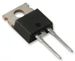
- Diode Case Style: TO-220
- Diode Configuration: Single
- Forward Voltage Max: 2V
- Forward Surge Current: 60A
- Average Forward Current: 29.2A
- Operating Temperature Max: 175°C
- Repetitive Peak Reverse Voltage: 600V
| Delivery and price | |
|---|---|
| Units per pack | 1 |
| Price | 0.392 € |
| Current stock | 10+ |
| Lead time | 30 days |
|**IDP15E60**<br> **FastSwitching Emitter Controlled Diode**<br> **Product Summary**<br>_V_RRM<br>600<br>V<br>_I_F<br>15<br>A<br>_V_F<br>1.5<br>V<br>_T_jmax<br>175<br>°C<br>**Features**<br>•600VEmitter Controlledtechnology<br>• Fast recovery<br>CinfineonO56<br>6— SF|**IDP15E60**<br> **FastSwitching Emitter Controlled Diode**<br> **Product Summary**<br>_V_RRM<br>600<br>V<br>_I_F<br>15<br>A<br>_V_F<br>1.5<br>V<br>_T_jmax<br>175<br>°C<br>**Features**<br>•600VEmitter Controlledtechnology<br>• Fast recovery<br>CinfineonO56<br>6— SF|| |---|---|---| |• Soft switching||| |• Low reverse recovery charge||| |• Low forward voltage||| |• Easy paralleling<br>PG-TO220-2||| |• Pb-free lead plating; RoHS compliant||| |• Halogen-free according to IEC61249-2-21||| |• Qualified according to JEDEC for target applications||| |**Pin 1**<br>**PIN 2**<br>**PIN 3**<br>C<br>A<br>-<br>**Marking**<br>D15E60<br>**Type**<br>**Package**<br>**Ordering Code**<br>IDP15E60<br>PG-TO220-2<br>-<br>yt||| |**Maximum Ratings**, at _T_j= 25 °C, unless otherwise specified||| |**Parameter**<br>**Symbol**<br>**Value**<br>**Unit**<br>**Parameter**<br>**Symbol**<br>**Value**<br>**Unit**<br>~~Ff~~||| |Repetitive peak reverse voltage<br>_V_RRM<br>600<br>V<br>Continous forward current<br>_T_C=25°C<br>_T_~~C~~=90°C<br>_I_F<br>29.2<br>19.6<br>A<br>Surge non repetitive forward current<br>~~_T_~~C~~=25°C,~~~~_t_~~p~~=10 ms, sine halfwave~~<br>_I_FSM<br>60<br>Maximum repetitive forward current<br>_I_FRM<br>45<br>Repetitivepeak reverse voltage<br>_V_R RM<br>600<br>V<br>Continuous forward current<br>_T_C= 25C<br>_T_C= 90C<br>_I_F<br>29.2<br>19.6<br>A<br>Surge non repetitive forward current<br>_T_C= 25C,_t_p= 10 ms, sine halfwave<br>_I_FS M<br>60<br>A<br>Maximum repetitive forward current<br>_T_C= 25C,_t_plimited by_t_j,max_, D_= 0.5<br>_I_FR M<br>45<br>A<br>~~—+—~~<br>~~a~~<br>~~a~~||| |_T_C=25°C,_t_plimited by_T_jmax,_D_=0.5<br>Power dissipation<br>_T_C=25°C<br>_T_C=90°C<br>_P_tot<br>83.3<br>47.2<br>W<br>Operating and storage temperature<br>_T_~~j ~~,_T_~~stg~~<br>-55...+175<br>°C<br>Soldering temperature<br>wavesoldering,1.6mm(0.063 in.) from case for 10s<br>_T_S<br>260<br>°C<br>Power dissipation<br>_T_C= 25C<br>_T_C= 90C<br>_P_t ot<br>83.3<br>47.2<br>W<br>Operating junction temperature<br>_T_j<br>-40…+175<br>°C<br>Storage temperature<br>_T_st g<br>-55...+150<br>Soldering temperature<br>1.6mm (0.063 in.) from case for 10 s<br>_T_S<br>260<br>~~Sa~~<br>~~ee~~<br>~~ee~~<br>~~a~~||| Rev. 2. 6 Page 1 20131205 |**IDP15E60**<br>**Thermal Characteristics**<br>**Parameter**<br>**Symbol**<br>**Values**<br>**Unit**<br>**min.**<br>**typ.**<br>**max.**<br>**Characteristics**<br>Cinfineon~~ee~~<br>~~er ee~~|**IDP15E60**<br>**Thermal Characteristics**<br>**Parameter**<br>**Symbol**<br>**Values**<br>**Unit**<br>**min.**<br>**typ.**<br>**max.**<br>**Characteristics**<br>Cinfineon~~ee~~<br>~~er ee~~|**IDP15E60**<br>**Thermal Characteristics**<br>**Parameter**<br>**Symbol**<br>**Values**<br>**Unit**<br>**min.**<br>**typ.**<br>**max.**<br>**Characteristics**<br>Cinfineon~~ee~~<br>~~er ee~~|**IDP15E60**<br>**Thermal Characteristics**<br>**Parameter**<br>**Symbol**<br>**Values**<br>**Unit**<br>**min.**<br>**typ.**<br>**max.**<br>**Characteristics**<br>Cinfineon~~ee~~<br>~~er ee~~|**IDP15E60**<br>**Thermal Characteristics**<br>**Parameter**<br>**Symbol**<br>**Values**<br>**Unit**<br>**min.**<br>**typ.**<br>**max.**<br>**Characteristics**<br>Cinfineon~~ee~~<br>~~er ee~~| |---|---|---|---|---| |Thermal resistance, junction - case|_R_thJC|-|-|1.8<br>K/W| |Thermal resistance, junction - ambient, leaded|_R_thJA|-|-|62| |SMD version, device on PCB:|_R_thJA|||| |@ min. footprint||-|-|62| |@ 6 cm2cooling area1)||-|35|-| |Reverse leakage current<br>_V_R=600V,_T_j=25°C<br>_V_R=600V,_T_j=150°C|_I_R|-<br>-|-<br>-|50<br>1250|μA| |---|---|---|---|---|---| |Forward voltage drop<br>_I_F=15A,_T_j=25°C<br>_I_F=15A,_T_j=150°C|_V_F|-<br>-|1.5<br>1.5|2<br>-|V| 1Device on 40mm*40mm*1.5mm epoxy PCB FR4 with 6cm² (one layer, 70 μm thick) copper area for drain connection. PCB is vertical without blown air. Rev. 2. 6 Page 2 20131205 |**Dynamic Characteristics**|~~er~~|~~er ee~~|~~ee~~|~~ee~~|~~ee~~| |---|---|---|---|---|---| |Reverse recovery time<br>_V_R=400V,_I_F=15A, d_i_F/d_t_=1000A/μs,_T_j=25°C<br>_V_R=400V,_I_F=15A, d_i_F/d_t_=1000A/μs,_T_j=125°C<br>_V_R=400V,_I_F=15A, d_i_F/d_t_=1000A/μs,_T_j=150°C|_t_rr|-<br>-<br>-|87<br>124<br>131|-<br>-<br>-|ns| |Peak reverse current<br>_V_R=400V,_I_F= 15A, d_i_F/d_t_=1000A/μs,_T_j=25°C<br>_V_R=400V,_I_F=15A, d_i_F/d_t_=1000A/μs,_T_j=125°C<br>_V_R=400V,_I_F=15A, d_i_F/d_t_=1000A/μs,_T_j=150°C|_I_rrm|-<br>-<br>-|13.7<br>16.4<br>19.3|-<br>-<br>-|A| |Reverse recovery charge<br>_V_R=400V,_I_F=15A, d_i_F/d_t_=1000A/μs,_T_j=25°C<br>_V_R=400V,_I_F=15A, d_i_F/d_t_=1000A/μs,_T_j=125°C<br>_V_R=400V,_I_F=15A, d_i_F/d_t_=1000A/μs,_T_j=150°C|_Q_rr|-<br>-<br>-|595<br>995<br>1104|-<br>-<br>-|nC| |Reverse recovery softness factor<br>_V_R=400V,_I_F=15A, d_i_F/d_t_=1000A/μs,_T_j=25°C<br>_V_R=400V,_I_F=15A, d_i_F/d_t_=1000A/μs,_T_j=125°C<br>_V_R=400V,_I_F=15A, d_i_F/d_t_=1000A/μs,_T_j=150°C|_S_|-<br>-<br>-|3.6<br>4.3<br>4.5|-<br>-<br>-|| Rev. 2. 6 Page 3 20131205 **IDP15E60** ## **1 Power dissipation** _P_ tot = _f_ ( _T_ C) parameter: Tj ≤ 175 °C ## **2 Diode forward current** _I_ F = f( _T_ C) parameter: _T_ j≤ 175°C **==> picture [483 x 600] intentionally omitted <==** **----- Start of picture text -----**<br> 90 30<br> W<br> A<br>70<br>60 SCEEEE) = 20 =LINCELE<br>50<br>et KR] Ef TEN] I<br>15<br>40 P| IN | | \<br>30 10<br>20 \ 5 \<br>10<br>SEEN 6OEEIN<br>0 0<br>25 50 75 100 125 °C 175 25 50 75 100 125 °C 175<br>T C T C<br>3 Typ. diode forward current 4 Typ. diode forward voltage<br>I F = f ( V F) V F = f ( T j)<br>50 2<br> V<br>30A<br> A ype<br>1.8<br>1.7<br>I eet EL<br>30 1.6<br>-55°C<br>25°C 1.5 15A<br>100°C<br>150°C<br>20 1.4 Lt} t+ |<br>1.3<br>7.5A<br>y77 eee<br>10 1.2<br>1.1<br>0 A”| |} 1 betes tte<br>0.5 1 1.5 V 2.5 -60 -20 20 60 100 °C 160<br>V F T j<br>tot<br>P I F<br>F<br>I F V<br>**----- End of picture text -----**<br> Rev. 2. 6 Page 4 20131205 **IDP15E60** ## **5 Typ. reverse recovery time** _t_ rr = _f_ (d _i_ F/d _t_ ) parameter: _V_ R = 400V, _T_ j = 125°C **==> picture [231 x 261] intentionally omitted <==** **----- Start of picture text -----**<br> 500<br> ns<br>Kop<br>400<br>NN<br>350<br>30A<br>300<br>15A<br>7.5A<br>250 AX<br>DNNes<br>200<br>f [NON<br>150 POSSE)<br>100<br>PCCP<br>50<br>to<br>aes<br>0<br>200 300 400 500 600 700 800 A/μs 1000<br> d i F/d t<br>t rr<br>**----- End of picture text -----**<br> ## **6 Typ. reverse recovery charge** _Q_ rr= _f_ (d _i_ F/d _t_ ) parameter: _V_ R = 400V, _T_ j = 125 °C **==> picture [231 x 258] intentionally omitted <==** **----- Start of picture text -----**<br> 1450 ee<br>nC<br>30A<br>ee ee ee ee<br>1250<br>FASE<br>1150<br>15A<br>1050<br>senseeoo<br>950<br>aoe<br>a<br>850<br>oP EERE<br>7.5A<br>750<br>ER See<br>650<br>EEE<br>oe<br>550<br>200 300 400 500 600 700 800 A/μs 1000<br>d i F/d t<br>rr<br>Q<br>**----- End of picture text -----**<br> ## **7 Typ. reverse recovery current** _I_ rr = _f_ (d _i_ F/d _t_ ) parameter: _V_ R = 400V, _T_ j = 125°C ## **8 Typ. reverse recovery softness factor** S = f(d _i_ F/d _t_ ) parameter: _V_ R = 400V, _T_ j = 125°C **==> picture [485 x 260] intentionally omitted <==** **----- Start of picture text -----**<br> 18 11<br> A<br>CECE NT TTI).<br>16 30A<br>15A<br>15<br>7.5A 9<br>14 EO ON<br>OG PNET<br>13 SO SNK 8 N<br>30A<br>12<br>ff — RONDO<br>11 a Amn 7 NN<br>10 15A<br>6<br>| 9 aLALaa ff VX ON—<br>8<br>5 7,5A<br>7<br>An SONS<br>6 = 4a Re<br>4<br>Poe PN ES<br>5<br>a ttt}<br>4 3 | etre<br>200 300 400 500 600 700 800 A/μs 1000 200 300 400 500 600 700 800 A/μs 1000<br> d i F/d t d i F/d t<br>I rr S<br>**----- End of picture text -----**<br> Rev. 2. 6 Page 5 20131205 **IDP15E60** ## **9 Max. transient thermal impedance** _Z_ thJC = _f_ ( _t_ p) parameter : _D_ = _t_ p/ _T_ **==> picture [231 x 268] intentionally omitted <==** **----- Start of picture text -----**<br> 10 1 IDP15E60<br>K/W COTLTT TCTC TTTTTTTn)TT)<br>TIT TTT TTT TTT TE TTT TTT<br>LTTE TMT TIME PETIT TIM TTT TTT<br>10 0 SNLecoCet PRSLeer—Eeeese Peee TTee<br>oerag Ce oh<br>mame<br>ine<br>10 -1 iis Il<br>=r<br>ee an< D = 0.50 cornyHHH<br>LTT AA TT ST TTT ITM<br>LOTTI TSS TPA TR 0.20 TM<br>AS Ht<br>0.10<br>0.05<br>-2<br>10 AU J<br>0.02<br>SeeCATeestiann eetSENteeeTTTest ITT)<br>LAT TC TT Te 0.01 Hn<br>Pty single pulse pina TT Ht<br>10 -3<br>10 [-7] 10 [-6] 10 [-5] 10 [-4] 10 [-3] 10 [-2] s 10 [0]<br>—_> t p<br>thJC<br>Z<br>**----- End of picture text -----**<br> Rev. 2. 6 Page 6 20131205 **IDP15E60** ## Package Outline: TO220-2 **==> picture [258 x 12] intentionally omitted <==** **----- Start of picture text -----**<br> Rev. 2. 6 Page 7<br>**----- End of picture text -----**<br> 20131205 **IDP15E60** **Published by** **Infineon Technologies AG 81726 Munich, Germany 81726 München, Germany © 2009 Infineon Technologies AG** **All Rights Reserved. Published by** **Infineon Technologies AGLegal Disclaimer** The information given in this document shall in no event be regarded as a guarantee of conditions or characteristics. **81726 Munich, Germany** With respect to any examples or hints given herein, any typical values stated herein and/or any information regarding **© 2013 Infineon Technologies AG** the application of the device, Infineon Technologies hereby disclaims any and all warranties and liabilities of any kind, including without limitation, warranties of non-infringement of intellectual property rights of any third party. **All Rights Reserved. Information** For further information on technology, delivery terms and conditions and prices, please contact the nearest Infineon Technologies Office (www.infineon.com). ## **Legal DisclaimerWarnings** ## **Warnings** TheDue to technical requirements, components may contain dangerous substances. For information on the types ininformation given in this document shall in no event be regarded as a guarantee of conditions or question, please contact the nearest Infineon Technologies Office. Infineon Technologies components may be used in characteristics. With respect to any examples or hints given herein, any typical values stated herein and/or life-support devices or systems only with the express written approval of Infineon Technologies, if a failure of such anycomponents can reasonably be expected to cause the failure of that life-support device or system or to affect the safetyinformation regarding the application of the device, Infineon Technologies hereby disclaims any and all warrantiesor effectiveness of that device or system. Life support devices or systems are intended to be implanted in the humanand liabilities of any kind, including without limitation, warranties of non-infringement of intellectual body or to support and/or maintain and sustain and/or protect human life. If they fail, it is reasonable to assume that the property rights of any third party. health of the user or other persons may be endangered. ## **Information** For further information on technology, delivery terms and conditions and prices, please contact the nearest Infineon Technologies Office ( **www.infineon.com** ) **.** ## **Warnings** Due to technical requirements, components may contain dangerous substances. For information on the types in question, please contact the nearest Infineon Technologies Office. The Infineon Technologies component described in this Data Sheet may be used in life-support devices or systems and/or automotive, aviation and aerospace applications or systems only with the express written approval of Infineon Technologies, if a failure of such components can reasonably be expected to cause the failure of that life-support, automotive, aviation and aerospace device or system or to affect the safety or effectiveness of that device or system. Life support devices or systems are intended to be implanted in the human body or to support and/or maintain and sustain and/or protect human life. If they fail, it is reasonable to assume that the health of the user or other persons may be endangered. Rev. 2. 6 Page 8 20131205
Updated at February 9, 2023
Infineon Technologies is a globally recognized leader in semiconductor solutions, renowned for driving innovation in power management, energy efficiency, and modern mobility. With a strong legacy of engineering excellence, the company provides highly reliable components designed to meet the rigorous demands of industrial, automotive, and advanced commercial applications. The core of our Infineon portfolio is centered on their industry-leading discrete semiconductors. We offer an extensive selection of single and dual MOSFETs, alongside a robust range of single IGBTs and advanced IGBT modules. These flagship power transistors are essential for high-efficiency power conversion and motor control, providing engineers with superior thermal performance and minimized switching losses. Beyond advanced field-effect transistors, the selection includes a comprehensive array of diodes and rectifiers, heavily featuring Schottky diodes, as well as fast-recovery and RF/PIN diodes. This power foundation is further supported by bipolar transistors, intelligent power modules, and thyristor SCR modules, delivering the critical building blocks required for complex power system designs. To support broader system integration, the portfolio also encompasses specialized solutions such as solid-state relays, AC/DC LED driver ICs, and Bluetooth communications modules. From high-power industrial rectifiers to wireless connectivity adapters, Infineon equips designers with the precision components needed to build efficient, scalable, and fully connected electronic systems.
About Novapart
Novapart is a B2B electronic component broker specialising in stock shortages and cost reduction. We source hard-to-find parts and identify compliant alternatives across a catalogue of 410,000+ components from 500+ manufacturers.
Learn more →Stock Shortage Specialist
When a component is unavailable, discontinued or has an unacceptable lead time, we tap into our network of vetted European and Asian distributors to source what you need — without compromising on quality or traceability.
Request a quote →Compliant Alternatives
We identify pin-to-pin, electrically equivalent substitutes that meet the same certifications (RoHS, AEC-Q100, REACH) as your original specification — validated against datasheets, not just part numbers. Often at a lower cost.
BOM Analysis service →