


IDFW40E65D1EXKSA1
Standard Recovery Diode, 650 V, 42 A, Single, 2.1 V, 76 ns
- Manufacturer: INFINEON
- Product type: Standard Recovery Rectifier Diodes
- Repetitive Reverse Voltage Vrrm Max:650V; Forward Current If(AV):42A; Diode Configuration:Single; Forward Voltage VF Max:2.1V; Reverse Recovery Time trr Max:76ns; Forward Surge Cur
- SVHC: No SVHC (25-Jun-2025)
- No. of Pins: 3Pins
- Product Range: -
- Qualification: -
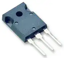
- Diode Case Style: TO-247
- Diode Configuration: Single
- Forward Voltage Max: 2.1V
- Forward Surge Current: -
- Reverse Recovery Time: 76ns
- Average Forward Current: 42A
- Operating Temperature Max: 175°C
- Repetitive Peak Reverse Voltage: 650V
| Delivery and price | |
|---|---|
| Units per pack | 100 |
| Price | 1.29 € |
| Current stock | 200+ |
| Lead time | 30 days |
IDFW40E65D1E
## **Features:**
**==> picture [158 x 65] intentionally omitted <==**
**----- Start of picture text -----**<br>
¢ Low forward voltage ( V F)<br>« Low reverse recovery charge ( Q rr)<br>« Low reverse recovery current ( I rrm)<br>¢ Softness factor >1<br>* Maximum junction temperature<br>*2500V RMS — electrical isolation,<br>**----- End of picture text -----**<br>
**==> picture [96 x 252] intentionally omitted <==**
**----- Start of picture text -----**<br>
A<br>C<br>,<br>2 3<br>Fully isolated package TO-247<br>**----- End of picture text -----**<br>
|**Type**|**_V_rrm**|**_I_f**|**_V_f** **_T_vj=25°C**|**_T_vjmax**|**Marking**|**Package**|
|---|---|---|---|---|---|---|
|IDFW40E65D1E|650V|40A|1.7V|175°C|D40E65D1E|PG-TO247-3-AI|
Datasheet www.infineon.com
2017-10-27
IDFW40E65D1E
**==> picture [86 x 38] intentionally omitted <==**
## Emitter�Controlled�Diode�Rapid�1�Advanced�Isolation
## **Table�of�Contents**
Description . . . . . . . . . . . . . . . . . . . . . . . . . . . . . . . . . . . . . . . . . . . . . . . . . . . . . . . . . . . . . . . . . . . . . . . . 1 Table of Contents . . . . . . . . . . . . . . . . . . . . . . . . . . . . . . . . . . . . . . . . . . . . . . . . . . . . . . . . . . . . . . . . . . . 2 Maximum Ratings . . . . . . . . . . . . . . . . . . . . . . . . . . . . . . . . . . . . . . . . . . . . . . . . . . . . . . . . . . . . . . . . . . . 3 Thermal Resistance . . . . . . . . . . . . . . . . . . . . . . . . . . . . . . . . . . . . . . . . . . . . . . . . . . . . . . . . . . . . . . . . . 3 Electrical Characteristics . . . . . . . . . . . . . . . . . . . . . . . . . . . . . . . . . . . . . . . . . . . . . . . . . . . . . . . . . . . . . . 3 Electrical Characteristics Diagrams . . . . . . . . . . . . . . . . . . . . . . . . . . . . . . . . . . . . . . . . . . . . . . . . . . . . . 5 Package Drawing . . . . . . . . . . . . . . . . . . . . . . . . . . . . . . . . . . . . . . . . . . . . . . . . . . . . . . . . . . . . . . . . . . . 8 Testing Conditions . . . . . . . . . . . . . . . . . . . . . . . . . . . . . . . . . . . . . . . . . . . . . . . . . . . . . . . . . . . . . . . . . . 9 Revision History . . . . . . . . . . . . . . . . . . . . . . . . . . . . . . . . . . . . . . . . . . . . . . . . . . . . . . . . . . . . . . . . . . . 10 Disclaimer . . . . . . . . . . . . . . . . . . . . . . . . . . . . . . . . . . . . . . . . . . . . . . . . . . . . . . . . . . . . . . . . . . . . . . . . 11
2
V�2.2 2017-10-27
Datasheet
IDFW40E65D1E
**==> picture [86 x 38] intentionally omitted <==**
## Emitter�Controlled�Diode�Rapid�1�Advanced�Isolation
## **Maximum�Ratings**
**For�optimum�lifetime�and�reliability,�Infineon�recommends�operating�conditions�that�do�not�exceed�80%�of�the�maximum�ratings�stated�in�this�datasheet.**
|**Parameter**|**Symbol**||**Value**|**Unit**|
|---|---|---|---|---|
|Repetitivepeakreversevoltage,_T_vj≥25°C|_V_RRM||650|V|
|Diodeforwardcurrent,limitedby_T_vjmax<br>_T_h=25°C<br>_T_h=65°C|_I_F||42.0<br>35.0|A|
|Diodepulsedcurrent,_t_plimitedby_T_vjmax|_I_Fpuls||120.0|A|
|Powerdissipation_T_h=25°C<br>Powerdissipation_T_h=65°C|_P_tot||78.0<br>57.0|W|
|Operating junction temperature|_T_vj|-40...+175||°C|
|Storage temperature|_T_stg|-55...+150||°C|
|Soldering temperature,<br>wave soldering1.6mm(0.063in.)from case for 10s|||260|°C|
|Mounting torque, M3 screw<br>Maximum of mounting processes: 3|_M_||0.6|Nm|
|IsolationvoltageRMS,_f_=50/60Hz,_t_=1min1)|_V_isol||2500|V|
## **Thermal�Resistance**
|**ThermalResistance**|||||||
|---|---|---|---|---|---|---|
|**Parameter**|**Symbol **|**Conditions**||**Value**||**Unit**|
||||**min.**|**typ.**|**max.**||
|**RthCharacteristics**|||||||
|Diode thermal resistance,2)<br>junction - heatsink|_R_th(j-h)||-|1.75|1.92|K/W|
|Thermal resistance<br>junction - ambient|_R_th(j-a)||-|-|65|K/W|
## **Electrical�Characteristic,�at�** _**T**_ **vj�=�25°C,�unless�otherwise�specified**
|**Parameter**|**Symbol **|**Conditions**||**Value**||**Unit**|
|---|---|---|---|---|---|---|
||||**min.**|**typ.**|**max.**||
|**StaticCharacteristic**|||||||
|Diode forward voltage|_V_F|_I_F=40.0A<br>_T_vj=25°C<br>_T_vj=175°C|-<br>-|1.70<br>1.75|2.10<br>-|V|
|Reverse leakage current|_I_R|_V_R=650V<br>_T_vj=25°C<br>_T_vj=175°C|-<br>-|-<br>350|40<br>-|µA|
## **Electrical�Characteristic,�at�** _**T**_ **vj�=�25°C,�unless�otherwise�specified**
|**Parameter**|**Symbol **|**Conditions**||**Value**||**Unit**|
|---|---|---|---|---|---|---|
||||**min.**|**typ.**|**max.**||
|**DynamicCharacteristic**|||||||
|Internal emitter inductance<br>measured 5mm (0.197 in.) from<br>case|_L_E||-|13.0|-|nH|
> 1) For a proper handling and assembly of the advanced isolation device in the application refer to the note at the package drawing.
> 2) At force on body F = 500N, Ta = 25ºC
3
V�2.2 2017-10-27
Datasheet
IDFW40E65D1E
**==> picture [86 x 38] intentionally omitted <==**
## Emitter�Controlled�Diode�Rapid�1�Advanced�Isolation
## **Switching�Characteristic,�Inductive�Load**
|**Parameter**|**Symbol **|**Conditions**||**Value**||**Unit**|
|---|---|---|---|---|---|---|
||||**min.**|**typ.**|**max.**||
|**DiodeCharacteristic,at****_T_vj=25°C**|||||||
|Diode reverse recoverytime|_t_rr|_T_vj=25°C,<br>_V_R=400V,<br>_I_F=40.0A,<br>_di_F_/dt_=1000A/µs,<br>_L_σ=75nH,<br>_C_σ=30pF,<br>Switch IKFW50N60DH3|-|76|-|ns|
|Diode reverse recoverycharge|_Q_rr||-|0.57|-|µC|
|Diodepeak reverse recoverycurrent|_I_rrm||-|11.0|-|A|
|Diode peak rate of fall of reverse<br>recoverycurrentduring_t_b|_di_rr_/dt_||-|-885|-|A/µs|
||||||||
|Diode reverse recoverytime|_t_rr|_T_vj=25°C,<br>_V_R=400V,<br>_I_F=40.0A,<br>_di_F_/dt_=300A/µs,<br>_L_σ=75nH,<br>_C_σ=30pF,<br>Switch IKFW50N60DH3|-|232|-|ns|
|Diode reverse recoverycharge|_Q_rr||-|0.52|-|µC|
|Diodepeak reverse recoverycurrent|_I_rrm||-|6.0|-|A|
|Diode peak rate of fall of reverse<br>recoverycurrentduring_t_b|_di_rr_/dt_||-|-130|-|A/µs|
## **Switching�Characteristic,�Inductive�Load**
|**Parameter**|**Symbol **|**Conditions**||**Value**||**Unit**|
|---|---|---|---|---|---|---|
||||**min.**|**typ.**|**max.**||
|**DiodeCharacteristic,at****_T_vj=175°C**|||||||
|Diode reverse recoverytime|_t_rr|_T_vj=175°C,<br>_V_R=400V,<br>_I_F=40.0A,<br>_di_F_/dt_=1000A/µs,<br>_L_σ=75nH,<br>_C_σ=30pF,<br>Switch IKFW50N60DH3|-|106|-|ns|
|Diode reverse recoverycharge|_Q_rr||-|1.51|-|µC|
|Diodepeak reverse recoverycurrent|_I_rrm||-|20.0|-|A|
|Diode peak rate of fall of reverse<br>recoverycurrentduring_t_b|_di_rr_/dt_||-|-760|-|A/µs|
||||||||
|Diode reverse recoverytime|_t_rr|_T_vj=175°C,<br>_V_R=400V,<br>_I_F=40.0A,<br>_di_F_/dt_=300A/µs,<br>_L_σ=75nH,<br>_C_σ=30pF,<br>Switch IKFW50N60DH3|-|228|-|ns|
|Diode reverse recoverycharge|_Q_rr||-|1.33|-|µC|
|Diodepeak reverse recoverycurrent|_I_rrm||-|9.8|-|A|
|Diode peak rate of fall of reverse<br>recoverycurrentduring_t_b|_di_rr_/dt_||-|-160|-|A/µs|
V�2.2 2017-10-27
Datasheet
4
IDFW40E65D1E
**==> picture [474 x 285] intentionally omitted <==**
**----- Start of picture text -----**<br>
80 45<br>40<br>70 ee ee ee eee<br>35<br>60 XE} EAL<br>sf NX]<br>30<br>- | de<br>: 50 |<br>25<br>ke N ef NN<br>40<br>{a}<br>d : ef NK<br>20<br>o x<br>30<br>SER ENGE See<br>15<br>eyo KE \<br>20<br>10<br>10<br>5<br>0 SERIES AS 0 P| ey |<br>25 50 75 100 125 150 175 25 50 75 100 125 150 175<br>T h , HEATSINK TEMPERATURE [°C] T h , HEATSINK TEMPERATURE [°C]<br>P tot I F<br>**----- End of picture text -----**<br>
> Figure 1. Power **temperature** ( _T_ j ≤ 175°C)
Figure 2.
**==> picture [482 x 286] intentionally omitted <==**
**----- Start of picture text -----**<br>
300<br>Tvj = 25°C, IF = 40A<br>CUT ETI TEM TMM TEE TIT TTT LUT Se Tvj = 175°C, IF = 40A a<br>MN ml = |<br>1<br>x HHI 250<br>WwO Se RTL RR cyeee D = 0.5 —_ ee ee<br>0.2<br>2 A 7 oa<br>ST TT A 0.1 200 oe Ce ee<br>0.05<br>Ae<br>ou 0.1 | 0.02 TU fF &<br>CEE Se 0.01 Ss PUAN]<br>w Co ee fe) 150<br>oi PTI CA Ae TT aT single pulse | || oO<br>= HT TF iy |i th PE AN<br>: ST TM Hil a \<br>a ei A eG 100 Nee<br>MC<br>2 0.01 Ti<br>s N/AFHI te zoTE -H Ry Ro__ iify ff Pf |NU————<br>FERRET<br>. TnTr | 50 Py PF<br>IT mien i: ET 1 TTT 2 TTT 3 iLTT 4 esate,TTT 5 ComrieTTT 6 TTll Pt<br>ri[K/W]: 0.341 0.56903 0.28633 0.34265 0.36597 0.023397<br>τ i[s]: 2.5E-4 1.6E-3 0.013093 0.158585 0.778817 15.94388<br>0.001 0<br>1E-7 1E-6 1E-5 1E-4 0.001 0.01 0.1 1 10 200 400 600 800 1000 1200<br>t p , PULSE WIDTH [s] di F /dt , DIODE CURRENT SLOPE [A/us]<br>t rr<br>h)th(j-<br>Z<br>**----- End of picture text -----**<br>
Figure 3. Diode function ( _D_ = _t_ p/T)
Figure 4.
( _V_ R=400V)
Datasheet
5
2017-10-27
IDFW40E65D1E
**==> picture [476 x 285] intentionally omitted <==**
**----- Start of picture text -----**<br>
1.8 LE 24 LE<br>Tvj = 25°C, IF = 40A Tvj = 25°C, IF = 40A<br>Tvj = 175°C, IF = 40A Tvj = 175°C, IF = 40A<br>1.6 EO) a<br>| 21 Ee<br>g 1.4 < pan<br>18<br>Ww “7 5<br>) 7 TT 7<br>z 1.2<br>3z 15 Z<br>> > 7<br>1.0<br>:9 co): 12 a rm a<br>0.8<br>ow w 7 .<br>9<br>0.6<br>> ><br>6<br>: TT és<br>0.4<br>3<br>| 0.2 Pf | ff ; “fof dL<br>0.0 0<br>200 400 600 800 1000 1200 200 400 600 800 1000 1200<br>di F /dt , DIODE CURRENT SLOPE [A/us] di F /dt , DIODE CURRENT SLOPE [A/us]<br>Q rr I rr<br>**----- End of picture text -----**<br>
Figure 5. Typical of diode ( _V_ R=400V)
Figure 6. Typical function ( _V_ R=400V)
**==> picture [472 x 322] intentionally omitted <==**
**----- Start of picture text -----**<br>
0 120<br>Tvj = 25°C, IF = 40A Tvj = 25°C<br>-100 Tvj = 175°C, IF = 40A 110 Tvj = 175°C<br>100<br>a -200 fo \ vi /<br>90<br>-300<br>$ ef] |se<br>80<br>5 \ =<br>res -400 \ Wyee<br>LL ow 70<br>Pf NN 8 Ef<br>Lu -500 \ oO 60 {_/<br>in m4<br>:Y oe<x 50<br>x -600 \ =<br>40<br>a eee<br>: -700 N re<br>30<br>Oo : i ee ee)<br>-800<br>20<br>-900<br>10<br>. oe) Ae<br>Po AY<br>-1000 0<br>N L<br>200 400 600 800 1000 1200 0.0 0.5 1.0 1.5 2.0 2.5 3.0 3.5<br>di F /dt , DIODE CURRENT SLOPE [A/us] V F , FORWARD VOLTAGE [V]<br>Figure 7. Typical peak reverse recovery current as a Figure 8. Typical diode forward current as a function<br>function of diode current slope forward voltage<br>( V R=400V)<br>I rr<br>I F<br>/dt<br>rr<br>dI<br>**----- End of picture text -----**<br>
6
Datasheet
2017-10-27
IDFW40E65D1E
**==> picture [233 x 286] intentionally omitted <==**
**----- Start of picture text -----**<br>
3.00<br>IF = 20A<br>IF = 40A<br>2.75 IF = 80A<br>2.50<br>Lu<br>Oo<br><x 2.25<br>Kk<br>I<br>><br>Q 2.00<br>m4<br><x<br>[a 1.75<br>LL<br>1.50<br>||<br>1.25<br>|<br>1.00<br>25 50 75 100 125 150 175<br>T j ,JUNCTION TEMPERATURE [°C]<br>F<br>V<br>**----- End of picture text -----**<br>
Figure 9.
Datasheet
7
2017-10-27
IDFW40E65D1E
**==> picture [86 x 38] intentionally omitted <==**
## Emitter�Controlled�Diode�Rapid�1�Advanced�Isolation
## **PG-TO247-3-AI (PGHSIP2473)**
**==> picture [408 x 570] intentionally omitted <==**
**----- Start of picture text -----**<br>
MILLIMETERS<br>DIMENSIONS<br>MIN. MAX.<br>A - 5.18 DOCUMENT NO.<br>A1 4.70 4.90 Z8B00186434<br>A2 2.23 2.59 REVISION<br>A3 0.20 0.28 02<br>b 1.10 1.30<br>c 0.50 0.70 SCALE 3:1<br>D 22.20 22.40 0 1 2 3 4 5 6 7 8mm<br>D1 16.96 17.16<br>E 15.70 15.90<br>E1 13.68 13.88 EUROPEAN PROJECTION<br>e 5.44<br>L 18.31 18.91<br>L1 2.76 2.96<br>øP 3.50 3.70<br>øP1 5.70 5.90 ISSUE DATE<br>Q 5.96 6.36 05.06.2018<br>**----- End of picture text -----**<br>
Note: For a proper handling and assembly of the advanced isolation device in the application the isolation layer must not be exposed to potential penetration via sharp implements or mechanical impacts/shocks, which exceed levels indicated in International Standard (IEC6006826 and IEC60068227). The advanced isolation device is intended only to be used assembled on an appropriate heatsink with recommended flatness of <20µm per 100mm and roughness of <10µm.
8
V�2.2 2017-10-27
Datasheet
IDFW40E65D1E
**==> picture [86 x 38] intentionally omitted <==**
## Emitter�Controlled�Diode�Rapid�1�Advanced�Isolation
## **Testing Conditions**
**==> picture [252 x 588] intentionally omitted <==**
**----- Start of picture text -----**<br>
V GE (t)<br>90% V GE<br>10% V GE t<br>I C (t)<br>90% I C 90% I C<br>10% I C 10% I C<br>t<br>V CE (t)<br>t<br>t d(off) t f t d(on) t r<br>Figure A.<br>V GE (t)<br>90% V GE<br>10% V GE<br>t<br>I C (t)<br>2% I C t<br>V CE (t)<br>t 2 t 4<br>E off [=] V CE x I C x d t E on [=] V CE x I C x d t<br>t 1 t 3 2% V CE<br>t<br>t 1 t 2 t 3 t 4<br>Figure B.<br>**----- End of picture text -----**<br>
**==> picture [189 x 170] intentionally omitted <==**
**----- Start of picture text -----**<br>
I,V<br>dI F /dt Qt rrrr== Qt aa++ tQ b b<br>a b<br>Q a Q b<br>dI<br>Figure C. Definition of diode switching<br>characteristics<br>**----- End of picture text -----**<br>
**==> picture [7 x 7] intentionally omitted <==**
**----- Start of picture text -----**<br>
t<br>**----- End of picture text -----**<br>
**==> picture [169 x 63] intentionally omitted <==**
Figure D.
**==> picture [7 x 4] intentionally omitted <==**
**----- Start of picture text -----**<br>
CC<br>**----- End of picture text -----**<br>
Figure E. **Dynamic test circuit** Parasitic inductance Ls, parasitic capacitor Cs, relief capacitor C ,r (only for ZVT switching)
9
V�2.2 2017-10-27
Datasheet
IDFW40E65D1E
**==> picture [86 x 38] intentionally omitted <==**
## Emitter�Controlled�Diode�Rapid�1�Advanced�Isolation
## **Revision�History**
IDFW40E65D1E
## **Revision:�2017-10-27,�Rev.�2.2**
## Previous Revision
|Revision|Date|Subjects(major changes since last revision)|
|---|---|---|
|2.1|2017-09-21|Final data sheet|
|2.2|2017-10-27|Update condition Fig.2|
10
V�2.2 2017-10-27
Datasheet
## **Trademarks**
## party.
## **Warnings**
Updated at April 22, 2026
Infineon Technologies is a globally recognized leader in semiconductor solutions, renowned for driving innovation in power management, energy efficiency, and modern mobility. With a strong legacy of engineering excellence, the company provides highly reliable components designed to meet the rigorous demands of industrial, automotive, and advanced commercial applications. The core of our Infineon portfolio is centered on their industry-leading discrete semiconductors. We offer an extensive selection of single and dual MOSFETs, alongside a robust range of single IGBTs and advanced IGBT modules. These flagship power transistors are essential for high-efficiency power conversion and motor control, providing engineers with superior thermal performance and minimized switching losses. Beyond advanced field-effect transistors, the selection includes a comprehensive array of diodes and rectifiers, heavily featuring Schottky diodes, as well as fast-recovery and RF/PIN diodes. This power foundation is further supported by bipolar transistors, intelligent power modules, and thyristor SCR modules, delivering the critical building blocks required for complex power system designs. To support broader system integration, the portfolio also encompasses specialized solutions such as solid-state relays, AC/DC LED driver ICs, and Bluetooth communications modules. From high-power industrial rectifiers to wireless connectivity adapters, Infineon equips designers with the precision components needed to build efficient, scalable, and fully connected electronic systems.
About Novapart
Novapart is a B2B electronic component broker specialising in stock shortages and cost reduction. We source hard-to-find parts and identify compliant alternatives across a catalogue of 410,000+ components from 500+ manufacturers.
Learn more →Stock Shortage Specialist
When a component is unavailable, discontinued or has an unacceptable lead time, we tap into our network of vetted European and Asian distributors to source what you need — without compromising on quality or traceability.
Request a quote →Compliant Alternatives
We identify pin-to-pin, electrically equivalent substitutes that meet the same certifications (RoHS, AEC-Q100, REACH) as your original specification — validated against datasheets, not just part numbers. Often at a lower cost.
BOM Analysis service →