
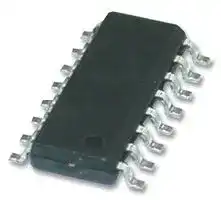


HVLED815PFTR
Led Driver, 1 Output, Constant Current/Voltage, 11.5V-23V in, 166kHz switch, NSOIC-16
- Manufacturer: STMICROELECTRONICS
- Product type: AC / DC LED Driver ICs
- Device Topology:Constant Current, Constant Voltage, Flyback; Input Voltage Min:11.5V; Input Voltage Max:23V; Output Voltage Max:-; Output Current Max:-; Switching Frequency:166kHz; No.
- MSL: MSL 3 - 168 hours
- SVHC: No SVHC (25-Jun-2025)
- Topology: Constant Current, Constant Voltage, Flyback
- IC Mounting: Surface Mount
- No. of Pins: 16Pins
- Product Range: -
- Qualification: -
- No. of Outputs: 1Outputs
- Device Topology: Constant Current, Constant Voltage, Flyback
- LED Driver Type: Isolated
- Driver Case Style: NSOIC
- IC Case / Package: NSOIC
- Input Voltage Max: 23V
- Input Voltage Min: 11.5V
- Output Current Max: -
- Output Voltage Max: -
- Switching Frequency: 166kHz
- Switching Frequency Typ: 166kHz
- Operating Temperature Max: 150°C
- Operating Temperature Min: -40°C
- Automotive Qualification Standard: -
| Delivery and price | |
|---|---|
| Units per pack | 2500 |
| Price | 0.786 € |
| Current stock | 10+ |
| Lead time | 30 days |
## **HVLED815PF** ## Offline LED driver with primary-sensing and high power factor up to 15 W **Datasheet** - **production data** ## **Applications** - AC-DC LED driver bulb replacement lamps up to 15 W, with high power factor - AC-DC LED drivers up to 15 W ## **Description** **==> picture [41 x 10] intentionally omitted <==** **----- Start of picture text -----**<br> SO16N<br>**----- End of picture text -----**<br> ## **Features** - High power factor capability (> 0.9) - 800 V, avalanche rugged internal 6 Power MOSFET - Internal high voltage startup - Primary sensing regulation (PSR) - ± 3% accuracy on constant LED output current - Quasi-resonant (QR) operation - Optocoupler not needed - Open or short LED string management The HVLED815PF device is a high voltage primary switcher intended for operating directly from the rectified mains with minimum external parts and enabling high power factor (> 0.90) to provide an efficient, compact and cost effective solution for LED driving. It combines a highperformance low voltage PWM controller chip and an 800 V, avalanche rugged Power MOSFET, in the same package. There is no need for the optocoupler thanks to the patented primary sensing regulation (PSR) technique. The device assures protection against LED string fault (open or short). **Table 1. Device summary** |**Order code**|**Package**|**Packaging**| |---|---|---| |HVLED815PF|SO16N|Tube| |HVLED815PFTR||Tape and reel| - Automatic self supply 1/34 February 2014 This is information on a product in full production. DocID023409 Rev 5 _www.st.com_ **Contents** **HVLED815PF** |**Contents**|**Contents**|| |---|---|---| |**1**|**Principle application circuit and block diagram . . . . . . . . . . . . . . . . . . . 4**|| ||1.1|Principle application circuit . . . . . . . . . . . . . . . . . . . . . . . . . . . . . . . . . . . . . 4| ||1.2|Block diagram . . . . . . . . . . . . . . . . . . . . . . . . . . . . . . . . . . . . . . . . . . . . . . . 6| |**2**|**Pin**|**description and connection diagrams . . . . . . . . . . . . . . . . . . . . . . . 7**| ||2.1|Pin description . . . . . . . . . . . . . . . . . . . . . . . . . . . . . . . . . . . . . . . . . . . . . . 7| ||2.2|Thermal data . . . . . . . . . . . . . . . . . . . . . . . . . . . . . . . . . . . . . . . . . . . . . . . 8| |**3**|**Electrical specifications . . . . . . . . . . . . . . . . . . . . . . . . . . . . . . . . . . . . . . 9**|| ||3.1|Absolute maximum ratings . . . . . . . . . . . . . . . . . . . . . . . . . . . . . . . . . . . . . 9| ||3.2|Electrical characteristics . . . . . . . . . . . . . . . . . . . . . . . . . . . . . . . . . . . . . . . 9| |**4**|**Device description . . . . . . . . . . . . . . . . . . . . . . . . . . . . . . . . . . . . . . . . . 14**|| ||4.1|Application information . . . . . . . . . . . . . . . . . . . . . . . . . . . . . . . . . . . . . . . 14| ||4.2|Power section and gate driver . . . . . . . . . . . . . . . . . . . . . . . . . . . . . . . . . 15| ||4.3|High voltage startup generator . . . . . . . . . . . . . . . . . . . . . . . . . . . . . . . . . 16| ||4.4|Secondary side demagnetization detection and triggering block . . . . . . . 17| ||4.5|Constant current operation . . . . . . . . . . . . . . . . . . . . . . . . . . . . . . . . . . . . 19| ||4.6|Constant voltage operation . . . . . . . . . . . . . . . . . . . . . . . . . . . . . . . . . . . 21| ||4.7|Voltage feedforward block . . . . . . . . . . . . . . . . . . . . . . . . . . . . . . . . . . . . 22| ||4.8|Burst mode operation at no load or very light load . . . . . . . . . . . . . . . . . . 24| ||4.9|Soft-start and starter block . . . . . . . . . . . . . . . . . . . . . . . . . . . . . . . . . . . . 25| ||4.10|Hiccup mode OCP . . . . . . . . . . . . . . . . . . . . . . . . . . . . . . . . . . . . . . . . . . 25| ||4.11|High power factor implementation . . . . . . . . . . . . . . . . . . . . . . . . . . . . . . 26| ||4.12|Layout recommendations . . . . . . . . . . . . . . . . . . . . . . . . . . . . . . . . . . . . . 29| |**5**|**Package information . . . . . . . . . . . . . . . . . . . . . . . . . . . . . . . . . . . . . . . . 31**|| |**6**|**Revision history . . . . . . . . . . . . . . . . . . . . . . . . . . . . . . . . . . . . . . . . . . . 33**|| 2/34 DocID023409 Rev 5 **List of figures** **HVLED815PF** ## **List of figures** |Figure|1.|Application circuit for high power factor LED driver - single range input. . . . . . . . . . . . . . . . 4| |---|---|---| |Figure|2.|Application circuit for standard LED driver . . . . . . . . . . . . . . . . . . . . . . . . . . . . . . . . . . . . . . 5| |Figure|3.|Block diagram . . . . . . . . . . . . . . . . . . . . . . . . . . . . . . . . . . . . . . . . . . . . . . . . . . . . . . . . . . . . 6| |Figure|4.|Pin connection (top view) . . . . . . . . . . . . . . . . . . . . . . . . . . . . . . . . . . . . . . . . . . . . . . . . . . . 7| |Figure|5.|OFF-state drain and source current test circuit . . . . . . . . . . . . . . . . . . . . . . . . . . . . . . . . . 11| |Figure|6.|COSSoutput capacitance variation . . . . . . . . . . . . . . . . . . . . . . . . . . . . . . . . . . . . . . . . . . . 12| |Figure|7.|Startup current test circuit. . . . . . . . . . . . . . . . . . . . . . . . . . . . . . . . . . . . . . . . . . . . . . . . . . 12| |Figure|8.|Quiescent current test circuit . . . . . . . . . . . . . . . . . . . . . . . . . . . . . . . . . . . . . . . . . . . . . . . 12| |Figure|9.|Operating supply current test circuit . . . . . . . . . . . . . . . . . . . . . . . . . . . . . . . . . . . . . . . . . . 13| |Figure|10.|Quiescent current during fault test circuit . . . . . . . . . . . . . . . . . . . . . . . . . . . . . . . . . . . . . . 13| |Figure|11.|Multi-mode operation of HVLED815PF (constant voltage operation). . . . . . . . . . . . . . . . . 15| |Figure|12.|High voltage start-up generator: internal schematic . . . . . . . . . . . . . . . . . . . . . . . . . . . . . . 16| |Figure|13.|Timing diagram: normal power-up and power-down sequences . . . . . . . . . . . . . . . . . . . . 17| |Figure|14.|DMG block, triggering block . . . . . . . . . . . . . . . . . . . . . . . . . . . . . . . . . . . . . . . . . . . . . . . . 17| |Figure|15.|Drain ringing cycle skipping as the load is progressively reduced . . . . . . . . . . . . . . . . . . . 18| |Figure|16.|Current control principle . . . . . . . . . . . . . . . . . . . . . . . . . . . . . . . . . . . . . . . . . . . . . . . . . . . 19| |Figure|17.|Constant current operation: switching cycle waveforms. . . . . . . . . . . . . . . . . . . . . . . . . . . 19| |Figure|18.|Voltage control principle: internal schematic . . . . . . . . . . . . . . . . . . . . . . . . . . . . . . . . . . . 22| |Figure|19.|Feedforward compensation: internal schematic . . . . . . . . . . . . . . . . . . . . . . . . . . . . . . . . . 23| |Figure|20.|Load-dependent operating modes: timing diagrams . . . . . . . . . . . . . . . . . . . . . . . . . . . . . 25| |Figure|21.|Hiccup mode OCP: timing diagram . . . . . . . . . . . . . . . . . . . . . . . . . . . . . . . . . . . . . . . . . . 26| |Figure|22.|High power factor implementation connection - single range input . . . . . . . . . . . . . . . . . . 27| |Figure|23.|Suggested routing for the LED driver . . . . . . . . . . . . . . . . . . . . . . . . . . . . . . . . . . . . . . . . . 30| |Figure|24.|SO16N package outline . . . . . . . . . . . . . . . . . . . . . . . . . . . . . . . . . . . . . . . . . . . . . . . . . . . 31| |Figure|25.|SO16N recommended footprint (dimensions are in mm) . . . . . . . . . . . . . . . . . . . . . . . . . . 32| 3/34 DocID023409 Rev 5 **==> picture [659 x 460] intentionally omitted <==** **----- Start of picture text -----**<br> 1 Principle application circuit and block diagram<br>1.1 Principle application circuit<br>Figure 1. Application circuit for high power factor LED driver - single range input<br>Lin T1 O utpout D iode Vout<br>VIN 1 10 J1<br>CON1<br>EMI FILTER Bridge Diode 2 9 R12<br>Rf 3 8 C12 C13<br>J2 F1 1A_DIP 4 Minimum Load<br>2 1 Cout Bulk Cout SMD<br>Lf 7<br>CON1<br>5 6 J3<br>Cf Cf CON1<br>TRANSFORMER<br>J4 Lf<br>CON1 Rf<br>C10<br>U1<br>VIN D 5 Rsense HVLED8xxPF<br>Y1 - SAFETY<br>RA Rsense 1 SOURCE 16<br>DRAIN<br>R1 (500 - 1.5k)CS 2 CS 15<br>220pF-1nF DRAIN<br>RB<br>C_Vcc (10uF MIN) VCC 3 VCC DRAIN 14<br>COS Filter (1uF) 4 GND DRAIN 13<br>ROS C_ILED (10uF) 5 ILED CS RPF D 4<br>CS Rf b DMG 6 DMG DMG Rdmg<br>Rf (8k-15k) Cf (330nF-680nF) 7 COMP VCC D 2<br>1N 4148<br>Cp (1n-10nF) NA 8 N.A. C_VCC (470nF) R-VCC (10-100ohm)<br>AM13207v1<br>4/34<br>3 Cin Cin<br>+ Csnubber Rsnubber<br>-<br>4<br>S nubber D iode<br>DocID023409 Rev 5<br>**----- End of picture text -----**<br> ## **Figure 2. Application circuit for standard LED driver** **==> picture [647 x 396] intentionally omitted <==** **----- Start of picture text -----**<br> T2 O utpout D iode1 Vout<br>VIN 1 10 J5<br>CON1<br>EMI FILTER Bridge Diode 2 9 R18<br>Rf 3 8 C16 C27<br>J7 F2 1A_DIP 4 Minimum Load<br>2 1 Cout Bulk Cout SMD<br>Lf 7<br>CON1<br>5 6 J6<br>Cf Cf CON1<br>TRANSFORMER<br>J8 Lf<br>CON1 Rf<br>C23<br>U2<br>Rsense HVLED8xxPF<br>Y1 - SAFETY<br>Rsense 1 SOURCE 16<br>DRAIN<br>2<br>CS 15<br>DRAIN<br>C_Vcc (10uF) VCC 3 VCC DRAIN 14<br>4 13<br>GND DRAIN<br>C_ILED (10uF) 5 ILED<br>Rf b DMG 6 DMG DMG Rdmg<br>Rf (8.2k-15k) Cf (330nF/680nF) 7 COMP VCC D 8<br>1N 4148<br>Cp (1nF/10nF) NA 8 N.A. C_VCC (470nF) R-VCC (10ohm)<br>AM13208v1<br>3<br>+<br>Cin<br>Csnubber Rsnubber<br>-<br>4<br>S nubber D iode<br>DocID023409 Rev 5<br>**----- End of picture text -----**<br> **==> picture [33 x 5] intentionally omitted <==** **----- Start of picture text -----**<br> AM13208v1<br>**----- End of picture text -----**<br> ## **1.2 Block diagram** **==> picture [659 x 394] intentionally omitted <==** **----- Start of picture text -----**<br> Figure 3. Block diagram<br>+ VIN<br>VCC HV start-up &<br>Supply Logic<br>DRAIN<br>LED<br>Vref<br>PROTECTION &<br>FEEDFORWARD<br>LOGIC<br>DEMAG<br>LOGIC<br>RDMG DMG CONSTANT DRIVING LOGIC<br>CURRENT<br>REGULATION<br>RFB 3.3 V VILED VCS<br>Vref 1 V<br>OCP<br>Constant Voltage RA<br>Regulation<br>COMP ILED GND CS R1 SOURCE<br>RCOMP CLED<br>CCOMP RSENSE<br>RPF ROS<br>AM13209v1<br>DocID023409 Rev 5<br>**----- End of picture text -----**<br> **HVLED815PF** **Pin description and connection diagrams** ## **2 Pin description and connection diagrams** ## **Figure 4. Pin connection (top view)** **==> picture [239 x 220] intentionally omitted <==** **----- Start of picture text -----**<br> SOURCE 11 1616 DRAIN<br>CS 22 1515 DRAIN<br>VCC 33 1414 DRAIN<br>GND 44 1313 DRAIN<br>ILED 5 12 N.C.<br>5 12<br>DMG 6 11 N.A.<br>6 11<br>COMP 77 1010 N.A.<br>N.A. 88 99 N.A.<br>**----- End of picture text -----**<br> **==> picture [33 x 6] intentionally omitted <==** **----- Start of picture text -----**<br> AM13210v1<br>**----- End of picture text -----**<br> ## **2.1 Pin description** ## **Table 2. Pin description** |||**Table 2. Pin description**| |---|---|---| |**No.**|**Name**|**Function**| |1|SOURCE|Source connection of the internal power section.| |2|CS|Current sense input.<br>Connect this pin to the SOURCE pin (through an R1resistor) to sense the current flowing in the<br>MOSFET through an RSENSEresistor connected to GND. The CS pin is also connected<br>through dedicated ROS, RPFresistors to the input and auxiliary voltage, in order to modulate<br>the input current flowing in the MOSFET according to the input voltage and therefore achieving<br>a high power factor. See_Section 4.11: High power factor implementation on page 26_for more<br>details.<br>The resulting voltage is compared with the voltage on the ILED pin to determine MOSFET turn-<br>off. The pin is equipped with 250 ns blanking time after the gate drive output goes high for<br>improved noise immunity. If a second comparison level located at 1 V is exceeded, the IC is<br>stopped and restarted after VCChas dropped below 5 V.| |3|VCC|Supply voltage of the device.<br>A capacitor, connected between this pin and ground, is initially charged by the internal high<br>voltage startup generator; when the device is running, the same generator keeps it charged in<br>case the voltage supplied by the auxiliary winding is not sufficient. This feature is disabled in<br>case a protection is tripped. A small bypass capacitor (100 nF typ.) to GND may be useful to<br>get a clean bias voltage for the signal part of the IC.| 7/34 DocID023409 Rev 5 **HVLED815PF** **Pin description and connection diagrams** **Table 2. Pin description (continued)** |||**Table 2. Pin description(continued)**| |---|---|---| |**No.**|**Name**|**Function**| |4|GND|Ground.<br>Current return for both the signal part of the IC and the gate drive. All of the ground<br>connections of the bias components should be tied to a trace going to this pin and kept<br>separate from any pulsed current return.| |5|ILED|Constant current (CC) regulation loop reference voltage.<br>An external capacitor CLEDis connected between this pin and GND. An internal circuit<br>develops a voltage on this capacitor that is used as the reference for the MOSFET’s peak drain<br>current during CC regulation. The voltage is automatically adjusted to keep the average output<br>current constant.| |6|DMG|Transformer demagnetization sensing for quasi-resonant operation and output voltage monitor.<br>A negative-going edge triggers the MOSFET turn-on, to achieve quasi-resonant operation<br>(zero voltage switching).<br>The pin voltage is also sampled-and-held right at the end of transformer demagnetization to get<br>an accurate image of the output voltage to be fed to the inverting input of the internal,<br>transconductance-type, error amplifier, whose non-inverting input is referenced to 2.5 V. The<br>maximum IDMGsunk/sourced current must not exceed ± 2 mA (AMR) in all the VINrange<br>conditions.<br>No capacitor is allowed between the pin and the auxiliary transformer.| |7|COMP|Output of the internal transconductance error amplifier. The compensation network is placed<br>between this pin and GND to achieve stability and good dynamic performance of the voltage<br>control loop.| |8|N. A.|Not available. These pins must be connected to GND.| |9 - 11|N. A.|Not available. These pins must be left not connected.| |12|N. C.|Not internally connected. Provision for clearance on the PCB to meet safety requirements.| |13 - 16|DRAIN|Drain connection of the internal power section.<br>The internal high voltage startup generator sinks current from this pin as well. Pins connected<br>to the internal metal frame to facilitate heat dissipation.| ## **2.2 Thermal data** ## **Table 3. Thermal data** ||**Table 3. Thermal data**||| |---|---|---|---| |**Symbol**|**Parameter**|**Max. value**|**Unit**| |RthJP|Thermal resistance, junction to pin|10|°C/W| |RthJA|Thermal resistance, junction to ambient|110|°C/W| |PTOT|Maximum power dissipation at TA= 50 °C|0.9|W| |TSTG|Storage temperature range|-55 to 150|°C| |TJ|Junction temperature range|-40 to 150|°C| 8/34 DocID023409 Rev 5 **Electrical specifications** **HVLED815PF** ## **3 Electrical specifications** ## **3.1 Absolute maximum ratings** **Table 4. Absolute maximum ratings** |**Symbol**|**Pin**|**Parameter**|**Value**|**Unit**| |---|---|---|---|---| |VDS|1, 13 - 16|Drain-to-source (ground) voltage|-1 to 800|V| |ID|1, 13 - 16|Drain current(1)|1|A| |Eav|1, 13 - 16|Single pulse avalanche energy<br>(TJ= 25 °C, ID= 0.7 A)|50|mJ| |VCC|3|Supply voltage (ICC< 25 mA)|Self limiting|V| |IDMG|6|Zero current detector current|±2|mA| |VCS|2|Current sense analog input|-0.3 to 3.6|V| |VCOMP|7|Analog input|-0.3 to 3.6|V| 1. Limited by maximum temperature allowed. ## **3.2 Electrical characteristics** **Table 5. Electrical characteristics[(1)][(2)]** |**Symbol**|**Parameter**|**Test condition**|**Min.**|**Typ.**|**Max.**|**Unit**| |---|---|---|---|---|---|---| |**Power section**||||||| |V(BR)DSS|Drain-source breakdown|ID< 100 µA; TJ= 25 °C|800|||V| |IDSS|OFF-state drain current|VDS= 750 V; TJ= 125 °C(3)<br>See_Figure 5_|||80|µA| |RDS(on)|Drain-source ON-state resistance|ID= 250 mA; TJ= 25 °C||6|7.4|| |||ID= 250 mA; TJ= 125 °C(3)|||14.8|| |COSS|Effective (energy related) output<br>capacitance|(3)See_Figure 6_||||| |**High voltage startup generator**||||||| |VSTART|Min. drain start voltage|ICHARGE< 100 µA|40|50|60|V| |ICHARGE|VCCstartup charge current|VDRAIN> VStart; VCC< VCCOn<br>TJ= 25 °C|4|5.5|7|mA| |||VDRAIN> VStart; VCC<VCCOn|+/- 10%|||| |VCC_RESTART|VCCrestart voltage<br>(VCCfalling)|(4)|9.5|10.5|11.5|V| |||After protection tripping||5||| |**Supply voltage**||||||| |VCC|Operating range|After turn-on|11.5||23|| |VCC_ON|Turn-on threshold|(4)|12|13|14|V| 9/34 DocID023409 Rev 5 **Electrical specifications** **HVLED815PF** **Table 5. Electrical characteristics[(1)][(2)] (continued)** |**Symbol**|**Parameter**|**Test condition**|**Min.**|**Typ.**|**Max.**|**Unit**| |---|---|---|---|---|---|---| |VCC_OFF|Turn-off threshold|(4)|9|10|11|V| |VZ|Internal Zener voltage|ICC= 20 mA|23|25|27|V| |**Supply current**||||||| |ICC_START-UP|Startup current|See_Figure 7_||200|300|µA| |Iq|Quiescent current|See_Figure 8_||1|1.4|mA| |ICC|Operating supply current<br>at 50 kHz|See_Figure 9_||1.4|1.7|mA| |Iq(fault)|Fault quiescent current|See_Figure 10_||250|350|µA| |**Startup timer**||||||| |TSTART|Start timer period||105|140|175|µs| |TRESTART|Restart timer period during burst<br>mode||420|500|700|µs| |**Demagnetization detector**||||||| |IDmgb|Input bias current|VDMG= 0.1 to 3 V||0.1|1|µA| |VDMGH|Upper clamp voltage|IDMG= 1 mA|3.0|3.3|3.6|V| |VDMGL|Lower clamp voltage|IDMG= - 1 mA|-90|-60|-30|mV| |VDMGA|Arming voltage|Positive-going edge|100|110|120|mV| |VDMGT|Triggering voltage|Negative-going edge|50|60|70|mV| |TBLANK|Trigger blanking time after<br>MOSFET turn-off|VCOMP 1.3 V||6||µs| |||VCOMP= 0.9 V||30||| |**Line feedforward**||||||| |RFF|Equivalent feedforward resistor|IDMG= 1 mA||45||| |**Transconductance error amplifier**||||||| |VREF|Voltage reference|TJ= 25 °C|2.45|2.51|2.57|V| |||(3)TJ= -25 to 125 °C<br>and VCC= 12 V to 23 V|2.4||2.6|| |gm|Transconductance|ICOMP= ± 10 µA<br>VCOMP= 1.65 V|1.3|2.2|3.2|ms| |Gv|Voltage gain|(5)Open loop||73||dB| |GB|Gain-bandwidth product|(5)||500||KHz| |ICOMP|Source current|VDMG= 2.3 V, VCOMP= 1.65 V|70|100||µA| ||Sink current|VDMG= 2.7 V, VCOMP= 1.65 V|400|750||µA| |VCOMPH|Upper COMP voltage|VDMG= 2.3 V||2.7||V| |VCOMPL|Lower COMP voltage|VDMG= 2.7 V||0.7||V| |VCOMPBM|Burst mode threshold|||1||V| |Hys|Burst mode hysteresis|||65||mV| 10/34 DocID023409 Rev 5 **Electrical specifications** **HVLED815PF** **Table 5. Electrical characteristics[(1)][(2)] (continued)** |**Symbol**|**Parameter**|**Test condition**|**Min.**|**Typ.**|**Max.**|**Unit**| |---|---|---|---|---|---|---| |**Current reference**||||||| |VILEDx|Maximum value|VCOMP= VCOMPL|1.5|1.6|1.7|V| |VCLED|Current reference voltage|(6)VILED= 0.41 V, VDMG= 0 V;<br>TJ= 25 °C|207.76|212|216.24|mV| |**Current sense**||||||| |tLEB|Leading-edge blanking|(5)||330||ns| |TD|Delay-to-output (H-L)|||90|200|ns| |VCSx|Max. clamp value|(4)dVcs/dt = 200 mV/µs|0.7|0.75|0.8|V| |VCSdis|Hiccup mode OCP level|(4)|0.92|1|1.08|V| 1. VCC = 14 V (unless otherwise specified). 2. Limits are production tested at TJ = TA = 25 °C, and are guaranteed by statistical characterization in the range TJ -25 to +125 °C. 3. Not production tested, guaranteed statistical characterization only. 4. Parameters tracking each other (in the same section). 5. Guaranteed by design. 6. Production tested only. ## **Figure 5. OFF-state drain and source current test circuit** **==> picture [461 x 201] intentionally omitted <==** **----- Start of picture text -----**<br> 14V<br>Idss<br>A<br>VDD DRAIN<br>2.5V + CURRENT Vin<br>CONTROL 750V<br>DMG -<br>COMP ILED GND CS SOURCE<br>AM13211v1<br>**----- End of picture text -----**<br> _Note: The measured IDSS is the sum between the current across the startup resistor and the effective MOSFET’s OFF-state drain current._ 11/34 DocID023409 Rev 5 **Electrical specifications** **HVLED815PF** ## **Figure 6. COSS output capacitance variation** ## **Figure 7. Startup current test circuit** **==> picture [320 x 143] intentionally omitted <==** **----- Start of picture text -----**<br> Iccstart-up A 11.8 V<br>VDD DRAIN<br>2.5V + CURRENT<br>CONTROL<br>DMG -<br>COMP ILED GND CS SOURCE<br>AM13213v1<br>**----- End of picture text -----**<br> ## **Figure 8. Quiescent current test circuit** **==> picture [328 x 186] intentionally omitted <==** **----- Start of picture text -----**<br> Iq_meas A 14V<br>VDD DRAIN<br>2.5V + CURRENT<br>CONTROL<br>DMG -<br>33k COMP ILED GND CS SOURCE<br>3V 0.8V<br>10k 0.2V<br>:<br>0.11 * 3V<br>Iq = 1dmeas — 3349, ~ 100yA<br>AM13214v1<br>**----- End of picture text -----**<br> 12/34 DocID023409 Rev 5 **Electrical specifications** **HVLED815PF** **Figure 9. Operating supply current test circuit** **==> picture [405 x 188] intentionally omitted <==** **----- Start of picture text -----**<br> 27k Icc A 15V 1.5K 2W<br>VDD DRAIN<br>220k<br>2.5V + CURRENT 150V<br>CONTROL<br>DMG -<br>10k 10k COMP ILED GND CS SOURCE<br>10<br>2.8V<br>5.6<br>50 kHz -5V<br>AM13215v1<br>**----- End of picture text -----**<br> _Note: The circuit across the DMG pin is used for switch on synchronization._ **Figure 10. Quiescent current during fault test circuit** **==> picture [405 x 184] intentionally omitted <==** **----- Start of picture text -----**<br> Iq(fault) A 14V<br>VDD DRAIN<br>2.5V + CURRENT<br>CONTROL<br>DMG -<br>COMP ILED GND CS SOURCE<br>AM13216v1<br>**----- End of picture text -----**<br> 13/34 DocID023409 Rev 5 **HVLED815PF** **Device description** ## **4 Device description** The HVLED815PF device is a high voltage primary switcher intended for operating directly from the rectified mains with minimum external parts to provide high power factor (> 0.90) and an efficient, compact and cost effective solution for LED driving. It combines a highperformance low voltage PWM controller chip and an 800 V, avalanche rugged Power MOSFET, in the same package. The PWM is a current mode controller IC specifically designed for ZVS (“Zero Voltage Switching”) flyback LED drivers, with constant output current (CC) regulation using primary sensing feedback (PSR). This eliminates the need for the optocoupler, the secondary voltage reference, as well as the current sense on the secondary side, while still maintaining a good LED current accuracy. Moreover, it guarantees a safe operation when short-circuit of one or more LEDs occurs. The device can also provide a constant output voltage regulation (CV): it allows the application to be able to work safely when the LED string opens due to a failure. In addition, the device offers the shorted secondary rectifier (i.e. LED string shorted due to a failure) or transformer saturation detection. Quasi-resonant operation is achieved by means of a transformer demagnetization sensing input that triggers MOSFET turn-on. This input serves also as both output voltage monitor, to perform CV regulation, and input voltage monitor, to achieve mains-independent CC regulation (line voltage feedforward). The maximum switching frequency is top limited below 166 kHz, so that at medium-light load a special function automatically lowers the operating frequency while still maintaining the operation as close to ZVS as possible. At very light load, the device enters a controlled burst mode operation that, along with the built-in high voltage startup circuit and the low operating current of the device, helps minimize the residual input consumption. Although an auxiliary winding is required in the transformer to correctly perform CV/CC regulation, the chip is able to power itself directly from the rectified mains. This is useful especially during CC regulation, where the flyback voltage generated by the winding drops. ## **4.1 Application information** The device is an off-line LED driver with all-primary sensing, based on quasi-resonant flyback topology, with high power factor capability. In particular, using different application schematic the device is able to provide a compact, efficient and cost-effective LED driver solution with high power factor (PF > 0.9 - see application schematic in _Figure 1 on page 4_ ) or with standard power factor (PF > 0.5/0.6 - see application schematic in _Figure 2 on page 5_ ), based on the specific application requirements. Referring to the application schematic in _Figure 1_ , the IC modulates the input current according to the input voltage providing the high power factor capability (PF > 0.9) keeping a good line regulation. This application schematic is intended for a single range input voltage. For wide range application a different reference schematic can be used; refer to AN4346 application note for further details. 14/34 DocID023409 Rev 5 **HVLED815PF** **Device description** Moreover, the device is able to work in different modes depending on the LED's driver load condition (see _Figure 11_ ): 1. QR mode at heavy load. Quasi-resonant operation lies in synchronizing MOSFET's turn-on to the transformer's demagnetization by detecting the resulting negative-going edge of the voltage across any winding of the transformer. Then the system works close to the boundary between discontinuous (DCM) and continuous conduction (CCM) of the transformer. As a result, the switching frequency is different for different line/load conditions (see the hyperbolic-like portion of the curves in _Figure 11_ ). Minimum turn-on losses, low EMI emission and safe behavior in short-circuit are the main benefits of this kind of operation. 2. Valley-skipping mode at medium/ light load. Depending on voltage on COMP pin, the device defines the maximum operating frequency of the converter. As the load is reduced, MOSFET's turn-on does not occur any more on the first valley but on the second one, the third one and so on. In this way the switching frequency is no longer increased (piecewise linear portion in _Figure 11_ ). 3. Burst mode with no or very light load. When the load is extremely light or disconnected, the converter enters a controlled on/off operation with constant peak current. Decreasing the load result in frequency reduction, which can go down even to few hundred hertz, thus minimizing all frequency-related losses and making it easier to comply with energy saving regulations or recommendations. Being the peak current very low, no issue of audible noise arises. **Figure 11. Multi-mode operation of HVLED815PF (constant voltage operation)** **==> picture [405 x 210] intentionally omitted <==** **----- Start of picture text -----**<br> fosc<br>Input voltage<br>f<br>sw Valley-skipping<br>mode<br>Burst-mode<br>Quasi-resonant mode<br>0<br>Pinmax<br>P<br>in AM13561v1<br>**----- End of picture text -----**<br> ## **4.2 Power section and gate driver** The power section guarantees safe avalanche operation within the specified energy rating as well as high dv/dt capability. The Power MOSFET has a VDSS of 800 V min. and a typical R of 6 . DS(on) The internal gate driver of the Power MOSFET is designed to supply a controlled gate current during both turn-on and turn-off in order to minimize common mode EMI. Under UVLO conditions an internal pull-down circuit holds the gate low in order to ensure that the Power MOSFET cannot be turned on accidentally. 15/34 DocID023409 Rev 5 **HVLED815PF** **Device description** ## **4.3 High voltage startup generator** _Figure 12_ shows the internal schematic of the high voltage start-up generator (HV generator). It includes an 800 V-rated N-channel MOSFET, whose gate is biased through the series of a 12 M resistor and a 14 V Zener diode, with a controlled, temperature compensated current generator connected to its source. The HV generator input is in common with the DRAIN pins, while its output is the supply pin of the device (VCC pin). A mains “UVLO” circuit (separated from the UVLO of the device that sense VCC) keeps the HV generator off if the drain voltage is below VSTART (50 V typical value). **Figure 12. High voltage start-up generator: internal schematic** **==> picture [405 x 220] intentionally omitted <==** **----- Start of picture text -----**<br> DRAIN<br>14V 12M<br>Mains UVLO<br>Vcc_OK<br>HV_EN IHV<br>VCC<br>CONTROL<br>Icharge<br>GND<br>AM13562v1<br>**----- End of picture text -----**<br> With reference to the timing diagram of _Figure 13_ , when power is applied to the circuit and the voltage on the input bulk capacitor is high enough, the HV generator is sufficiently biased to start operating, thus it will draw about 5.5 mA (typical) to the VCC capacitor. Most of this current will charge the bypass capacitor connected between the VCC pin and ground and make its voltage rise linearly. As soon as the VCC pin voltage reaches the VCC_ON turn on threshold (13 V typ.) the chip starts operating, the internal Power MOSFET is enabled to switch and the HV generator is cut off by the Vcc_OK signal asserted high. The IC is powered by the energy stored in the VCC capacitor. The chip is able to power itself directly from the rectified mains: when the voltage on the VCC pin falls below VCC_RESTART (10.5 V typ.), during each MOSFET's off-time the HV current generator is turned on and charges the supply capacitor until it reaches the VCC_ON threshold. In this way, the self-supply circuit develops a voltage high enough to sustain the operation of the device. This feature is useful especially during constant current (CC) regulation, when the flyback voltage generated by the auxiliary winding alone may not be able to keep VCC pin above VCC_RESTART. 16/34 DocID023409 Rev 5 **HVLED815PF** **Device description** **Figure 13. Timing diagram: normal power-up and power-down sequences** **==> picture [405 x 223] intentionally omitted <==** **----- Start of picture text -----**<br> VIN<br>VStart<br>t<br>VCC<br>VccON<br>Vccrestart<br>t<br>DRAIN<br>t<br>ICHARGE<br>5.5 mA<br>Power-on Normal operation Normal operation Power-off t<br>CV mode CC mode<br>AM13563v1<br>**----- End of picture text -----**<br> ## **4.4 Secondary side demagnetization detection and triggering block** The demagnetization detection (DMG) and triggering blocks switch on the Power MOSFET if a negative-going edge falling below 50 mV is applied to the DMG pin. To do so, the triggering block must be previously armed by a positive-going edge exceeding 100 mV. This feature is used to detect transformer demagnetization for QR operation, where the signal for the DMG input is obtained from the transformer's auxiliary winding used also to supply the IC. **Figure 14. DMG block, triggering block** **==> picture [405 x 204] intentionally omitted <==** **----- Start of picture text -----**<br> Rdmg DMG<br>DMG BLANKING<br>CLAMP TIME<br>Rf b STARTER<br>Aux<br>TURN-ON<br>LOGIC S<br>110mV Q To Driv er<br>60mV<br>From CC/CV Block LEB R<br>From OCP<br>AM13564v1<br>-<br>+<br>**----- End of picture text -----**<br> The triggering block is blanked after MOSFET's turn-off to prevent any negative-going edge that follows leakage inductance demagnetization from triggering the DMG circuit 17/34 DocID023409 Rev 5 **HVLED815PF** **Device description** erroneously. This TBLANK blanking time is dependent on the voltage on COMP pin: it is TBLANK = 30 µs for VCOMP = 0.9 V, and decreases almost linearly down to TBLANK = 6 µs for VCOMP = 1.3 V. The voltage on the pin is both top and bottom limited by a double clamp, as illustrated in the internal diagram of the DMG block of _Figure 14_ . The upper clamp is typically located at 3.3 V, while the lower clamp is located at -60 mV. The interface between the pin and the auxiliary winding will be a resistor divider. Its resistance ratio as well as the individual resistance values will be properly chosen (see _Section 4.6_ , _Section 4.7 on page 22_ and _Section 4.11 on page 26_ ). Please note that the maximum IDMG sunk/sourced current has to not exceed ±2 mA (AMR) in all the VIN range conditions. No capacitor is allowed between DMG pin and the auxiliary transformer. The switching frequency is top limited below 166 kHz, as the converter's operating frequency tends to increase excessively at light load and high input voltage. A starter block is also used to start up the system, that is, to turn on the MOSFET during converter power-up, when no or a too small signal is available on the DMG pin. The starter frequency is 2 kHz if COMP pin is below burst mode threshold, i.e. 1 V, while it becomes 8 kHz if this voltage exceeds this value. After the first few cycles initiated by the starter, as the voltage developed across the auxiliary winding becomes large enough to arm the DMG circuit, MOSFET's turn-on will start to be locked to transformer demagnetization, hence setting up QR operation. The starter is activated also when the IC is in “Constant Current” regulation and the output voltage is not high enough to allow the DMG triggering. If the demagnetization completes - hence a negative-going edge appears on the DMG pin - after a time exceeding time TBLANK from the previous turn-on, the MOSFET will be turned on again, with some delay to ensure minimum voltage at turn-on. If, instead, the negativegoing edge appears before TBLANK has elapsed, it will be ignored and only the first negative-going edge after TBLANK will turn-on the MOSFET. In this way one or more drain ringing cycles will be skipped (““valley-skipping mode”, _Figure 15_ ) and the switching frequency will be prevented from exceeding 1/TBLANK. **Figure 15. Drain ringing cycle skipping as the load is progressively reduced** **==> picture [405 x 121] intentionally omitted <==** **----- Start of picture text -----**<br> VDS VDS VDS<br>TON TFW TW t t t<br>TOSC TOSC TOSC<br>Pin = Pin' Pin = Pin'' < Pin' Pin = Pin''' < Pin''<br>(limit condition)<br>AM13565v1<br>**----- End of picture text -----**<br> _Note: That when the system operates in valley skipping-mode, uneven switching cycles may be observed under some line/load conditions, due to the fact that the OFF-time of the MOSFET is allowed to change with discrete steps of one ringing cycle, while the OFF-time needed for cycle-by-cycle energy balance may fall in between. Thus one or more longer switching cycles will be compensated by one or more shorter cycles and vice versa. However, this mechanism is absolutely normal and there is no appreciable effect on the performance of the converter or on its output voltage._ 18/34 DocID023409 Rev 5 **HVLED815PF** **Device description** ## **4.5 Constant current operation** _Figure 16_ presents the principle used for controlling the average output current of the flyback converter. The voltage of the auxiliary winding is used by the demagnetization block to generate the control signal for the internal MOSFET switch Q. A resistor R in series with it absorbs a current equal to VILED/R, where VILED is the voltage developed across the capacitor CLED capacitor. The flip-flop's output is high as long as the transformer delivers current on secondary side. This is shown in _Figure 17_ . ## **Figure 16. Current control principle** **==> picture [405 x 235] intentionally omitted <==** **----- Start of picture text -----**<br> .<br>Iref<br>VILED To PWM Logic<br>CC<br>R From CS pin<br>Q<br>S<br>Q<br>Rdmg DMG DEMAG R<br>LOGIC<br>Icled<br>Rf b<br>Aux ILED<br>CLED<br>AM13566v1<br>-<br>+<br>**----- End of picture text -----**<br> **Figure 17. Constant current operation: switching cycle waveforms** **==> picture [405 x 216] intentionally omitted <==** **----- Start of picture text -----**<br> IPRIM<br>t<br>ISEC<br>t<br>TONSEC<br>Q<br>t<br>ICLED<br>IREF<br>t<br>VILED/R<br>T<br>AM13567v1<br>**----- End of picture text -----**<br> 19/34 DocID023409 Rev 5 **HVLED815PF** **Device description** The capacitor CLED has to be chosen so that its voltage VILED can be considered as a constant. Since it is charged and discharged by currents in the range of some ten µA (IREF = 20 µA typ.) at the switching frequency rate, a capacitance value in the range 4.7 - 10 nF is suited for switching frequencies in the ten kHz. When high power factor schematic is implemented, a higher capacitor value should be used (i.e. 1 µF - 10 µF). The average output current IOUT can be expressed as: ## **Equation 1** **==> picture [130 x 32] intentionally omitted <==** Where _ISEC_ is the secondary peak current, _TONSEC_ is the conduction time of the secondary side and _T_ is the switching period. Taking into account the transformer ratio N between primary and secondary side, ISEC can also be expressed as a function of the primary peak current IPRIM: ## **Equation 2** As in steady state the average current ICLED: ## **Equation 3** **==> picture [256 x 31] intentionally omitted <==** Which can be solved for VILED: ## **Equation 4** **==> picture [228 x 32] intentionally omitted <==** where _VCLED_ = R * IREF and it is internally defined (0.2 V typical - see _Table 5: Electrical characteristics on page 9_ ). The VILED pin voltage is internally compared with the CS pin voltage (constant current comparator): ## **Equation 5** Combining (1), (2), (4), and (5) the average output current results: ## **Equation 6** **==> picture [228 x 33] intentionally omitted <==** 20/34 DocID023409 Rev 5 **HVLED815PF** **Device description** _Equation 6_ shows that the average output current IOUT does not depend anymore on the input voltage VIN or the output voltage VOUT, neither on transformer inductance values. The external parameters defining the output current are the transformer ratio _n_ and the sense resistor _RSENSE_ . _Equation 6_ is valid for both standard and high power factor implementation. ## **4.6 Constant voltage operation** The IC is specifically designed to work in primary regulation and the output voltage is sensed through a voltage partition of the auxiliary winding, just before the auxiliary rectifier diode. _Figure 18_ shows the internal schematic of the constant voltage mode and the external connections. Due to the parasitic wires resistance, the auxiliary voltage is representative of the output just when the secondary current becomes zero. For this purpose, the signal on DMG pin is sampled-and-held at the end of transformer's demagnetization to get an accurate image of the output voltage and it is compared with the error amplifier internal reference voltage VREF (2.51 V typ. - see _Table 5: Electrical characteristics on page 9_ ). During the MOSFET's OFF-time the leakage inductance resonates with the drain capacitance and a damped oscillation is superimposed on the reflected voltage. The S/H logic is able to discriminate such oscillations from the real transformer's demagnetization. When the DMG logic detects the transformer's demagnetization, the sampling process stops, the information is frozen and compared with the error amplifier internal reference. The internal error amplifier is a transconductance type and delivers an output current proportional to the voltage unbalance of the two outputs: the output generates the control voltage that is compared with the voltage across the sense resistor, thus modulating the cycle-by-cycle peak drain current. The COMP pin is used for the frequency compensation: usually, an RC network, which stabilizes the overall voltage control loop, is connected between this pin and ground. As a result, the output voltage VOUT at zero-load (i.e. no LED on the LED driver output) can be selected trough the RFB resistor in according to _Equation 7_ : ## **Equation 7** **==> picture [198 x 43] intentionally omitted <==** Where _NAUX_ and _NSEC_ are the auxiliary and secondary turn's number respectively. The RDMG resistor value can be defined depending on the application parameters (see _Section 4.7: Voltage feedforward block_ ). 21/34 DocID023409 Rev 5 **HVLED815PF** **Device description** ## **Figure 18. Voltage control principle: internal schematic** **==> picture [405 x 197] intentionally omitted <==** **----- Start of picture text -----**<br> Rdmg DMG<br>S/H<br>To PWM Logic<br>EA<br>CV<br>Rf b 2.5V<br>Aux DEMAG<br>LOGIC<br>From CS pin<br>COMP<br>R<br>C<br>AM13568v1<br>-<br>-<br>+<br>+<br>**----- End of picture text -----**<br> ## **4.7 Voltage feedforward block** The current control structure uses the VCLED voltage to define the output current, according to _Equation 6_ in _Section 4.5_ . Actually, the constant current comparator will be affected by an internal propagation delay TD, which will switch off the MOSFET with a peak current than higher the foreseen value. This current overshoot will be equal to: ## **Equation 8** **==> picture [198 x 33] intentionally omitted <==** The previous terms introduce a small error on the calculated average output current setpoint, depending on the input voltage. The HVLED815PF device implements a line feedforward function, which solves the issue by introducing an input voltage dependent offset on the current sense signal, in order to adjust the cycle-by-cycle current limitation. The internal schematic is shown in _Figure 19_ . 22/34 DocID023409 Rev 5 **HVLED815PF** **Device description** ## **Figure 19. Feedforward compensation: internal schematic** **==> picture [378 x 177] intentionally omitted <==** **----- Start of picture text -----**<br> DRAIN<br>Rdmg DMG<br>Feedforward .<br>Logic<br>Rfb CC<br>Aux IFF Block PWM<br>CC LOGIC<br>Rff<br>CS SOURCE<br>Rsense<br>AM13569v1<br>-<br>+<br>**----- End of picture text -----**<br> During MOSFET's ON-time the current sourced from DMG pin is mirrored inside the “Feedforward Logic” block in order to provide a feedforward current, IFF. Such “feedforward current” is proportional to the input voltage according to _Equation 9_ : ## **Equation 9** Where _m_ is the primary-to-auxiliary turns ratio. According to the schematic in _Figure 19_ , the voltage on the non-inverting comparator will be: ## **Equation 10** The offset introduced by feedforward compensation will be: ## **Equation 11** As RFF >> RSENSE, the previous one can be simplified as: ## **Equation 12** This offset is proportional to VIN and it is used to compensate the current overshoot, according to _Equation 13_ : 23/34 DocID023409 Rev 5 **HVLED815PF** **Device description** ## **Equation 13** **==> picture [220 x 35] intentionally omitted <==** Finally, the RDMG resistor can be calculated as follows: ## **Equation 14** **==> picture [220 x 33] intentionally omitted <==** In this case the peak drain current does not depend on input voltage anymore, and as a consequence the average output current IOUT does not depend from the VIN input voltage. When high power factor is implemented (see _Section 4.11_ ), the feedforward current has to be minimized because the line regulation is assured by the external offset circuitry (see _Figure 1: Application circuit for high power factor LED driver - single range input on page 4_ ). The maximum value is limited by the minimum IDMG internal current needed to guarantee the correct functionality of the internal circuitry: ## **Equation 15** **==> picture [341 x 35] intentionally omitted <==** ## **4.8 Burst mode operation at no load or very light load** When the voltage at the COMP pin falls 65 mV is below the internally fixed threshold VCOMPBM, the IC is disabled with the MOSFET kept in OFF state and its consumption reduced at a lower value to minimize VCC capacitor discharge. In this condition the converter operates in burst mode (one pulse train every TSTART = 500 µs), with minimum energy transfer. As a result of the energy delivery stop, the output voltage decreases: after 500 µs the controller switches on the MOSFET again and the sampled voltage on the DMG pin is compared with the internal reference VREF. If the voltage on the EA output, as a result of the comparison, exceeds the VCOMPL threshold, the device restarts switching, otherwise it stays OFF for another 500 µs period. In this way the converter will work in burst mode with a nearly constant peak current defined by the internal disable level. A load decrease will then cause a frequency reduction, which can go down even to few hundred hertz, thus minimizing all frequency-related losses and making it easier to comply with energy saving regulations. This kind of operation, shown in the timing diagrams of _Figure 20_ along with the others previously described, is noise-free since the peak current is low. 24/34 DocID023409 Rev 5 **HVLED815PF** **Device description** **==> picture [405 x 228] intentionally omitted <==** **----- Start of picture text -----**<br> Figure 20. Load-dependent operating modes: timing diagrams<br>COMP<br>50 mV hysteresis (Hys)<br>VCOMPL<br>IDS<br>t<br>t<br>Normal-mode Burst-mode Normal-mode<br>AM13570v1<br>**----- End of picture text -----**<br> ## **4.9 Soft-start and starter block** The soft-start feature is automatically implemented by the constant current block, as the primary peak current will be limited from the voltage on the CLED capacitor. During the startup, as the output voltage is zero, the IC will start in constant current (CC) mode with no high peak current operations. In this way the voltage on the output capacitor will increase slowly and the soft-start feature will be ensured. Actually the CLED value is not important to define the soft-start time, as its duration depends on others circuit parameters, like transformer ratio, sense resistor, output capacitors and load. The user will define the best appropriate value by experiments. ## **4.10 Hiccup mode OCP** The device is also protected against short-circuit of the secondary rectifier, short-circuit on the secondary winding or a hard-saturated flyback transformer. An internal comparator monitors continuously the voltage on CS pin and activates a protection circuitry if this voltage exceeds an internally fixed threshold VCSdis (1 V typ. - see _Table 5: Electrical characteristics on page 9_ ). To distinguish an actual malfunction from a disturbance (e.g. induced during ESD tests), the first time the comparator is tripped, the protection circuit enters a “warning state”. If in the subsequent switching cycle the comparator is not tripped, a temporary disturbance is assumed and the protection logic will be reset in its idle state; if the comparator will be tripped again a real malfunction is assumed and the device will be stopped. This condition is latched as long as the device is supplied. While it is disabled, however, no energy is coming from the self-supply circuit; hence the voltage on the VCC capacitor will decay and cross the UVLO threshold after some time, which clears the latch. The internal start-up generator is still off, then the VCC voltage still needs to go below its restart voltage before the VCC capacitor is charged again and the device restarted. 25/34 DocID023409 Rev 5 **HVLED815PF** **Device description** Ultimately, this will result in a low-frequency intermittent operation (hiccup mode operation), with very low stress on the power circuit. This special condition is illustrated in the timing diagram of _Figure 21_ . ## **Figure 21. Hiccup mode OCP: timing diagram** **==> picture [405 x 212] intentionally omitted <==** **----- Start of picture text -----**<br> VCC<br>Secondary diode is shorted here<br>VccON<br>VccOFF<br>Vccrest<br>VCS t<br>Vcsdis 1 V<br>VDS t<br>Two switching cycles<br>t<br>AM13571v1<br>**----- End of picture text -----**<br> ## **4.11 High power factor implementation** Referring to the principle application schematic in _Figure 1 on page 4_ , two contributions are added on the CS pin in order to implement the high power factor capability (trough RPF resistor) and keeping a good line regulation (trough ROS resistor). The application schematic on _Figure 1_ is intended for a single range input voltage. For wide range application a different reference schematic can be used; refer to AN4346 application note for further details. Through the RPF resistor a contribution proportional to the input voltage is added on the CS pin: as a consequence the input current is proportional to the input voltage during the line period, implementing a high power factor correction. The contribution proportional to the input voltage is generated using the auxiliary winding, as a consequence a diode in series to the RPF resistor is needed. Through the ROS resistor a positive contribution proportional to the average value of the input voltage is added on the CS pin in order to keep a good line regulation. The voltage contribution proportional to the average value of the input voltage is generated trough the low pass filter RA/RB resistor and COS capacitor. A diode in series to the RA/RB resistor is suggested to avoid the discharge of COS capacitor in any condition. The R1 resistor between CS and SOURCE pin is needed to add on the CS pin also the contribution proportional the output current trough the RSENSE resistor. 26/34 DocID023409 Rev 5 **HVLED815PF** **Device description** **Figure 22. High power factor implementation connection - single range input** **==> picture [371 x 201] intentionally omitted <==** **----- Start of picture text -----**<br> DRAIN<br>T<br>Rdmg DMG<br>Feedf orward .<br>Logic1<br>=H<br>Rf b CC<br>Aux IFF Block1 CC LOGIC2PWM<br>S SL<br>—<br>Rf f<br>CS C1 C1 SOURCE<br>RPF R1<br>— _|<br>ROS Rsense<br>VIN (after bridge diode) RA RB<br>a a in<br>COS<br>AM13572v1<br>-<br>+<br>**----- End of picture text -----**<br> The components selection flow starts from the RDMG resistor: this resistor has to be selected in order to minimize the internal feedforward effect. The maximum selectable value is limited by the minimum internal current circuitry IDMG needed to guarantee the correct functionality of the internal circuitry: ## **Equation 16** where _NAUX_ and _NPRIM_ are the auxiliary and primary turn's number respectively and VIN_MIN is the minimum rms input voltage of the application (i.e. 88 V for 110 Vac or 175 V for 230 Vac range). The RFB resistor defines the VOUT output voltage value in the open circuit condition (no-load condition, i.e. no LED on the output of LED driver) and it can be selected using the following relationship: ## **Equation 17** where _NAUX_ and _NSEC_ are the auxiliary and secondary turn's number respectively and VREF is the internal reference voltage (VREF = 2.51 V typ - see _Table 5: Electrical characteristics on page 9_ ). The R1 resistor is typically selected in the range of 500 - 1.5 k in order to minimize the internal feedforward effect and to minimize the power dissipation on the RA/RB resistor offset circuitry. 27/34 DocID023409 Rev 5 **HVLED815PF** **Device description** The RA, RB, ROS resistors are selected to add a positive offset on CS pin in order to keep a good line regulation over the input voltage range and cab be selected using _Equation 18_ : ## **Equation 18** **==> picture [316 x 39] intentionally omitted <==** Where _VOS_TYP_ is the desired voltage across COS capacitor applying the VIN_TYP typical input voltage (i.e. VIN_TYP = 220 V for 176/264 Vac input range); _FSW_ is the switching frequency and can be estimated using _Equation 19_ , where fT and fR are the transition and resonant frequency respectively: ## **Equation 19** **==> picture [193 x 58] intentionally omitted <==** ## **Equation 20** **==> picture [404 x 51] intentionally omitted <==** ## **Equation 21** where _CD_ is the total equivalent capacitor afferent at the drain node. Based on the desired voltage across the COS capacitor and calculated ROS resistor, then the sum of RA and RB can then calculated as a results of partitioning divider: ## **Equation 22** **==> picture [341 x 36] intentionally omitted <==** Using the previous ROS resistor value the RPF resistor can be estimated using _Equation 23_ : ## **Equation 23** **==> picture [405 x 59] intentionally omitted <==** 28/34 DocID023409 Rev 5 **HVLED815PF** **Device description** Finally the current sense resistor RSENSE can be estimated in order to select the desiderated average output current value: ## **Equation 24** **==> picture [136 x 33] intentionally omitted <==** where _VCLED_ is internally defined (0.2 V typical - see _Table 5: Electrical characteristics on page 9_ ). ## **System design tips** Starting from the previous estimated components value, further fine-tuning on the real LED driver board could be necessary and it can be easily done considering that: - Decreasing/increasing the RPF resistor value, the power factor effect increases/decreases. - Decreasing/increasing the ROS resistor value, the line regulation effect increases/decreases. - Decreasing/increasing the ROS resistor value, the RA + RB resistors value should be increased/decreased to keep the desiderated voltage across the COS capacitor ( _Equation 22_ ). - Decreasing/increasing the RSENSE resistor value the average output current increases/decreases ( _Equation 24_ ). ## **4.12 Layout recommendations** A proper printed circuit board layout is essential for correct operation of any switch-mode converter and this is true for the HVLED815PF device as well. Careful component placing, correct traces routing, appropriate traces widths and compliance with isolation distances are the major issues. In particular: - Current sense resistor (RSENSE) should be connected as close as possible to the SOURCE pin, maintaining the trace for the GND as short as possible. - Resistor connected on CS pin (ROS, RPF, R1) should be connected as close as possible to the pin. - Compensation network (RCOMP, CCOMP) should be connected as close as possible to the COMP pin, maintaining the trace for the GND as short as possible. - Signal ground should be routed separately from power ground, as well from the sense resistor trace. - DMG partition resistors (RDMG, RFB) should be connected as close as possible to the DMG pin, minimizing the equivalent parasitic capacitor on DMG pin. 29/34 DocID023409 Rev 5 **HVLED815PF** **Device description** ## **Figure 23. Suggested routing for the LED driver** **==> picture [398 x 211] intentionally omitted <==** **----- Start of picture text -----**<br> AC<br>AC<br>VCC DRAIN<br>RDMG<br>DMG<br>RFB COMP ILED GND SOURCE CS RPF ROS<br>RCOMP R1<br>CCOMP CLED<br>RSENSE<br>AM13573v1<br>**----- End of picture text -----**<br> 30/34 DocID023409 Rev 5 **Package information** **HVLED815PF** ## **5 Package information** In order to meet environmental requirements, ST offers these devices in different grades of ECOPACK[®] packages, depending on their level of environmental compliance. ECOPACK specifications, grade definitions and product status are available at: _www.st.com_ . ECOPACK is an ST trademark. ## **Figure 24. SO16N package outline** **==> picture [384 x 497] intentionally omitted <==** **----- Start of picture text -----**<br> 0016020_F<br>**----- End of picture text -----**<br> 31/34 DocID023409 Rev 5 **Package information** **HVLED815PF** **Table 6. SO16N package mechanical data** ||**Table 6. SO16Npackage mechanical data**|**Table 6. SO16Npackage mechanical data**|**Table 6. SO16Npackage mechanical data**| |---|---|---|---| |**Symbol**|**Dimensions (mm)**||| ||**Min.**|**Typ.**|**Max.**| |A|||1.75| |A1|0.10||0.25| |A2|1.25||| |b|0.31||0.51| |c|0.17||0.25| |D|9.80|9.90|10.00| |E|5.80|6.00|6.20| |E1|3.80|3.90|4.00| |e||1.27|| |h|0.25||0.50| |L|0.40||1.27| |k|0||8°| |ccc|||0.10| ## **Figure 25. SO16N recommended footprint (dimensions are in mm)** **==> picture [405 x 291] intentionally omitted <==** 32/34 DocID023409 Rev 5 **HVLED815PF** **Revision history** ## **6 Revision history** 22-Oct **Table 7. Document revision history** |**Date**|**Revision**|**Changes**| |---|---|---| |26-Jul-2012|1|Initial release.| |29-Aug-2012|2|Added_Table 2: Pin description on page 7_.| |23-Oct-2012|3|Modified TJvalue on_Table 3: Thermal data_.<br>Updated TJvalue in note 2 (below_Table 5: Electrical characteristics_).<br>Minor text changes.| |31-Jan-2013|4|Added sections from_4.1_to_4.12_.<br>Modified_Figure 1: Application circuit for high power factor LED driver_<br>_- single range input_and_Figure 2: Application circuit for standard LED_<br>_driver_.| |18-Feb-2014|5|Updated_Section : Features on page 1_(replaced ± 5% by ± 3% in<br>accuracy on constant LED output current).<br>Updated_Table 5: Electrical characteristics_(updated Test condition,<br>Values and Units of VCLEDsymbol, added note_6._below_Table 5_).<br>Updated_Section 5: Package information_(reversed order of<br>_Figure 24: SO16N package outline_and_Table 6: SO16N package_<br>_mechanical data_, updated titles of_Figure 24_and_Table 6_).<br>Minor modifications throughout document.| 33/34 DocID023409 Rev 5 **HVLED815PF** ## **Please Read Carefully:** Information in this document is provided solely in connection with ST products. STMicroelectronics NV and its subsidiaries (“ST”) reserve the right to make changes, corrections, modifications or improvements, to this document, and the products and services described herein at any time, without notice. All ST products are sold pursuant to ST’s terms and conditions of sale. Purchasers are solely responsible for the choice, selection and use of the ST products and services described herein, and ST assumes no liability whatsoever relating to the choice, selection or use of the ST products and services described herein. No license, express or implied, by estoppel or otherwise, to any intellectual property rights is granted under this document. If any part of this document refers to any third party products or services it shall not be deemed a license grant by ST for the use of such third party products or services, or any intellectual property contained therein or considered as a warranty covering the use in any manner whatsoever of such third party products or services or any intellectual property contained therein. **UNLESS OTHERWISE SET FORTH IN ST’S TERMS AND CONDITIONS OF SALE ST DISCLAIMS ANY EXPRESS OR IMPLIED WARRANTY WITH RESPECT TO THE USE AND/OR SALE OF ST PRODUCTS INCLUDING WITHOUT LIMITATION IMPLIED WARRANTIES OF MERCHANTABILITY, FITNESS FOR A PARTICULAR PURPOSE (AND THEIR EQUIVALENTS UNDER THE LAWS OF ANY JURISDICTION), OR INFRINGEMENT OF ANY PATENT, COPYRIGHT OR OTHER INTELLECTUAL PROPERTY RIGHT.** **ST PRODUCTS ARE NOT DESIGNED OR AUTHORIZED FOR USE IN: (A) SAFETY CRITICAL APPLICATIONS SUCH AS LIFE SUPPORTING, ACTIVE IMPLANTED DEVICES OR SYSTEMS WITH PRODUCT FUNCTIONAL SAFETY REQUIREMENTS; (B) AERONAUTIC APPLICATIONS; (C) AUTOMOTIVE APPLICATIONS OR ENVIRONMENTS, AND/OR (D) AEROSPACE APPLICATIONS OR ENVIRONMENTS. WHERE ST PRODUCTS ARE NOT DESIGNED FOR SUCH USE, THE PURCHASER SHALL USE PRODUCTS AT PURCHASER’S SOLE RISK, EVEN IF ST HAS BEEN INFORMED IN WRITING OF SUCH USAGE, UNLESS A PRODUCT IS EXPRESSLY DESIGNATED BY ST AS BEING INTENDED FOR “AUTOMOTIVE, AUTOMOTIVE SAFETY OR MEDICAL” INDUSTRY DOMAINS ACCORDING TO ST PRODUCT DESIGN SPECIFICATIONS. PRODUCTS FORMALLY ESCC, QML OR JAN QUALIFIED ARE DEEMED SUITABLE FOR USE IN AEROSPACE BY THE CORRESPONDING GOVERNMENTAL AGENCY.** Resale of ST products with provisions different from the statements and/or technical features set forth in this document shall immediately void any warranty granted by ST for the ST product or service described herein and shall not create or extend in any manner whatsoever, any liability of ST. ST and the ST logo are trademarks or registered trademarks of ST in various countries. Information in this document supersedes and replaces all information previously supplied. The ST logo is a registered trademark of STMicroelectronics. All other names are the property of their respective owners. © 2014 STMicroelectronics - All rights reserved STMicroelectronics group of companies Australia - Belgium - Brazil - Canada - China - Czech Republic - Finland - France - Germany - Hong Kong - India - Israel - Italy - Japan - Malaysia - Malta - Morocco - Philippines - Singapore - Spain - Sweden - Switzerland - United Kingdom - United States of America ## **www.st.com** 34/34 DocID023409 Rev 5
Updated at April 10, 2026
STMicroelectronics is a global leader in the semiconductor industry, recognized for developing highly integrated, energy-efficient solutions that power modern electronics. With a strong focus on innovation, ST provides a comprehensive portfolio of microelectronics that address the demanding requirements of industrial, automotive, communications, and consumer applications. Our extensive selection of STMicroelectronics components is built around a robust lineup of discrete semiconductors and circuit protection devices. We offer a wide variety of single MOSFETs, Schottky diodes, and fast and ultrafast recovery rectifier diodes, designed to deliver exceptional efficiency and thermal performance in power management and conversion systems. For robust circuit protection, our inventory features hundreds of transient voltage suppressors and TVS diodes that safeguard sensitive electronic components against destructive voltage spikes. In addition to core power discretes like TRIACs, SCRs, bipolar transistors, and single IGBTs, our STMicroelectronics range includes specialized integrated passive filters and MEMS sensors. Furthermore, ST offers advanced integrated passive devices, such as baluns and RF filters, which utilize high-quality monolithic RF IPD processes on glass or high-resistance silicon substrates. These components provide competitive cost structures, reduced power losses, and simplified RFIC-to-antenna matching, ensuring optimal system performance and delivering the reliability required for next-generation wireless and power designs.
About Novapart
Novapart is a B2B electronic component broker specialising in stock shortages and cost reduction. We source hard-to-find parts and identify compliant alternatives across a catalogue of 410,000+ components from 500+ manufacturers.
Learn more →Stock Shortage Specialist
When a component is unavailable, discontinued or has an unacceptable lead time, we tap into our network of vetted European and Asian distributors to source what you need — without compromising on quality or traceability.
Request a quote →Compliant Alternatives
We identify pin-to-pin, electrically equivalent substitutes that meet the same certifications (RoHS, AEC-Q100, REACH) as your original specification — validated against datasheets, not just part numbers. Often at a lower cost.
BOM Analysis service →