
Image not available
Illustrative purposes only

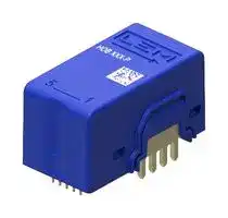
HOB 130-P
Current Sensor, Voltage Output, 1.2 % Accuracy, -250 to 250 A, 4.6 to 5.5 V
⚠️ Reference pricing provided. In case of supply shortages, we will connect you with our trusted procurement partners to ensure your project's continuity.
- Manufacturer: LEM
- Product type: Current Sensors
- SVHC: No SVHC (25-Jun-2025)
- Accuracy: ± 1.2%
- Accuracy %: 1.2%
- Product Range: HOB-P Series
- Response Time: 100ns
- Primary Current: 130A
- Sensor Mounting: Through Hole
- Measured Current: AC / DC / Pulsed
- Sensor Output Type: Voltage
- Supply Voltage Range: 4.6V to 5.5V
- Secondary Signal Type: 2.5V
- Supply Voltage DC Max: 5.5V
- Supply Voltage DC Min: 4.6V
- Current Sensor Technology: Open Loop, Hall Effect
- Operating Temperature Max: 105°C
- Operating Temperature Min: -40°C
- Current Measuring Range AC: -250A to 250A
- Current Measuring Range DC: -250A to 250A
| Delivery and price | |
|---|---|
| Units per pack | 50 |
| Price | 11.18 € |
| Current stock | 100+ |
| Lead time | 30 days |
Datasheet

**Current Transducer HOB-P/SP1 series**

_I_ **= 50 … 130 A** P N

**Ref: HOB 50-P/SP1, HOB 75-P/SP1, HOB 100-P/SP1, HOB 130-P/SP1**

**For the electronic measurement of current: DC, AC, pulsed..., with galvanic separation between the primary and the secondary circuit.**

## **Features**

- ●Open loop multi-range current transducer

- ●Voltage output

- ●Single power supply +5 V

- ●Galvanic separation between primary and secondary circuit

- ●Low power consumption

- ●Compact design for THT PCB mounting

- ●Factory calibrated.

## **Special feature**

- ●Level shifting.

## **Advantages**

- ●Low offset temperature drift

- ●Creepage / clearance > 11 mm

- ●Very short delay time < 200 ns

- ●High cut-off frequency > 1 MHz

- ●Enhanced immunity.

## **Applications**

- ●AC variable speed and servo motor drives

- ●Static converters for DC motor drives

- ●Battery supplied applications

- ●Uninterruptible Power Supplies (UPS)

- ●Switched Mode Power Supplies (SMPS)

- ●Combiner box

- ●Solar inverter on DC side of the inverter (MPPT)

- ●Plasma cutter, welding

- ●Charging station.

## **Standards**

- ●IEC 61010-1: 2017

- ●IEC 61010-2-30: 2017

- ●IEC 61800-3: 2017

- ●IEC 61800-5-1: 2007

- ●IEC 62109-1: 2010

- ●UL 508: 2018.

## **Application Domain**

- ●Industrial.

Page 1/12 LEM International SA Route du Nant-d’Avril, 152 1217 Meyrin www.lem.com

N°97.W9.25.001.0; N°97.W9.30.001.0; N°97.W9.34.001.0; N°97.W9.37.001.0

LEM reserves the right to carry out modifications on its transducers, in order to improve them.

23May2022/Version 1

**HOB-P/SP1 series**

## **Safety**

## ⚠ Caution

If the device is used in a way that is not specified by the manufacturer, the protection provided by the device may be compromised. Always inspect the electronics unit and connecting cable before using this product and do not use it if damaged. Mounting assembly shall guarantee the maximum primary conductor temperature, fulfill clearance and creepage distance, minimize electric and magnetic coupling, and unless otherwise specified can be mounted in any orientation. This device is not intended for outdoor use.

## Caution, risk of electrical shock

This transducer must be used in limited-energy secondary circuits SELV according to IEC 61010-1, in electric/electronic equipment with respect to applicable standards and safety requirements in accordance with the manufacturer’s operating specifications.

Use caution during installation and use of this product; certain parts of the module can carry hazardous voltages and high currents (e.g. power supply, primary conductor).

Ignoring this warning can lead to injury and or/or cause serious damage.

De-energize all circuits and hazardous live parts before installing the product.

All installations, maintenance, servicing operations and use must be carried out by trained and qualified personnel practicing applicable safety precautions.

This transducer is a build-in device, whose hazardous live parts must be inaccessible after installation. This transducer must be mounted in a suitable end-enclosure.

Besides make sure to have a distance of minimum 30 mm between the primary terminals of the transducer and other neighboring components.

## Main supply must be able to be disconnected.

Never connect or disconnect the external power supply while the primary circuit is connected to live parts. Never connect the output to any equipment with a common mode voltage to earth greater than 30 V.

Always wear protective clothing and gloves if hazardous live parts are present in the installation where the measurement is carried out.

This transducer is a built-in device, not intended to be cleaned with any product. Nevertheless if the user must implement cleaning or washing process, validation of the cleaning program has to be done by himself. When defining soldering process, please use no cleaning process only.

## ESD susceptibility

The product is susceptible to be damaged from an ESD event and the personnel should be grounded when handling it.

Do not dispose of this product as unsorted municipal waste. Contact a qualified recycler for disposal.

Although LEM applies utmost care to facilitate compliance of end products with applicable regulations during LEM product design, use of this part may need additional measures on the application side for compliance with regulations regarding EMC and protection against electric shock. Therefore LEM cannot be held liable for any potential hazards, damages, injuries or loss of life resulting from the use of this product.

Compliance with EU directives.

## ⎓

Direct current power supply.

Underwriters Laboratory Inc. recognized component

Page 2/12 LEM International SA Route du Nant-d’Avril, 152 1217 Meyrin www.lem.com

LEM reserves the right to carry out modifications on its transducers, in order to improve them.

23May2022/Version 1

**HOB-P/SP1 series**

## **Absolute maximum ratings**

**==> picture [512 x 20] intentionally omitted <==**

**----- Start of picture text -----**<br>
Parameter Symbol Unit Value<br>**----- End of picture text -----**<br>


||**Symbol**|**Unit**|**Unit**|
|---|---|---|---|
|||||
|Supply voltage (not destructive)|_U_C|V|5.5|
|Primary conductor temperature|_T_B|°C|120|
|Electrostatic discharge voltage (HBM - Human Body<br>Model)|_U_ESD|kV|2|


Stresses above these ratings may cause permanent damage. Exposure to absolute maximum ratings for extended periods may degrade reliability.

## **UL 508: Ratings and assumptions of certification**

File # E189713 Volume: 2 Section: 19

## **Standards**

- ●CSA C22.2 NO. 14-18 INDUSTRIAL CONTROL EQUIPMENT - Edition 13

- ●UL 508 STANDARD FOR INDUSTRIAL CONTROL EQUIPMENT - Edition 18

## **Ratings**

**==> picture [512 x 20] intentionally omitted <==**

**----- Start of picture text -----**<br>
Parameter Symbol Unit Value<br>**----- End of picture text -----**<br>


|**Parameter**|**Symbol**|**Unit**|**Value**|**Value**|
|---|---|---|---|---|
||||||
|Primary involved potential||V AC/DC|600||
|Max surrounding air temperature|_T_A|°C|100|105|
|Primary current|_I_P|A|130<br>100||
|Secondary supply voltage|_U_C|V DC|5||
|Output voltage|_U_out|V|0 to 5||
|Current consumption (max)|_I_C|mA|26||


## **Conditions of acceptability**

When installed in the end-use equipment, consideration shall be given to the following:

- _1 - The secondary circuit pin terminals have not been evaluated for field wiring._

- _2 - Low voltage control circuit shall be supplied by an isolating 5 V DC source._

- _3 - This product is intended to be mounted on a printed wiring board._

## **Marking**

Only those products bearing the UR Mark should be considered to be Listed or Recognized and covered under UL's Follow-Up Service. Always look for the Mark on the product.

Page 3/12 LEM International SA Route du Nant-d’Avril, 152 1217 Meyrin www.lem.com

LEM reserves the right to carry out modifications on its transducers, in order to improve them.

23May2022/Version 1

**HOB-P/SP1 series**

## **Insulation coordination**

**==> picture [512 x 22] intentionally omitted <==**

**----- Start of picture text -----**<br>
Parameter Symbol Unit Value Comment<br>**----- End of picture text -----**<br>


|**Parameter**|**Symbol**|**Unit**|**Value**|**Comment**|
|---|---|---|---|---|
||||||
|RMS voltage for AC insulation test 50/60 Hz/1 min|_U_d|kV|4.4||
|Impulse withstand voltage 1.2/50 µs|_U_Ni|kV|9.6||
|Partial discharge test voltage (_q_m< 10 pC)|_U_t|V|1500|Primary / Secondary|
|Clearance (pri. - sec.)|_d_CI|mm|> 11|Shortest distance through<br>air|
|Creepage distance (pri. - sec.)|_d_Cp|mm|> 11|Shortest path along device<br>body|
|Clearance (pri. - sec.)||mm|> 11|When mounted on PCB<br>with recommended layout|
|Case material||||V0 according to UL 94|
|Comparative tracking index|_CTI_||600||
|Application example||V|600|Reinforced insulation, non<br>uniform feld according to<br>IEC 61800-5-1, CAT III<br>PD2|
|Application example||V|1000|Basic insulation non<br>uniform feld according to<br>IEC 61800-5-1,<br>CAT III PD2|
|Application example||V|600|Simple insulation, non<br>uniform feld according to<br>UL 508,<br>CAT III PD2|


## **Environmental and mechanical characteristics**

**==> picture [512 x 22] intentionally omitted <==**

**----- Start of picture text -----**<br>
Parameter Symbol Unit Min Typ Max Comment<br>**----- End of picture text -----**<br>


|**Parameter**|**Symbol**|**Unit**|**Min**|**Typ**|**Max**|**Comment**|
|---|---|---|---|---|---|---|
|Ambient operating temperature|_T_A|°C|−40||105||
|Ambient storage temperature|_T_A st|°C|−40||105||
|Mass|_m_|g||30|||
|Relative Humidity|_RH_|%|||95||
|Altitude||m|||20001)||


Note:[1) ] Insulation coordination at 2000 m.

Page 4/12 LEM International SA Route du Nant-d’Avril, 152 1217 Meyrin www.lem.com

LEM reserves the right to carry out modifications on its transducers, in order to improve them.

23May2022/Version 1

## **Electrical data HOB 50-P/SP1**

## **HOB-P/SP1 series**

At _T_ A = 25 °C, _U_ C = +3.3 V, _R_ L = 10 kΩ unless otherwise noted (see Min, Max, typ. definition paragraph in page 9).

**==> picture [511 x 659] intentionally omitted <==**

**----- Start of picture text -----**<br>
Parameter Symbol Unit Min Typ Max Comment<br>Primary nominal RMS current I P N A 50<br>A −125 125 See Level shifting<br>Primary current, measuring range I P M conditions on page 10<br>Number of primary turns N P 1<br>Primary jumper resistance @ +25 °C R P mΩ 0.06<br>Primary jumper resistance @ +120 °C R P mΩ 0.076<br>Supply voltage U C V 4.6 5 5.5<br>Current consumption I C mA 18 22 26<br>Reference voltage (output) U ref V 2.48 2.5 2.52 Internal reference<br>Reference voltage (input range) U ref V 0.4 U C−0.4 External reference  U ref (IN)<br>Over operating temperature<br>Output voltage range @  I P M U out −  U ref V −4 4 range<br>U ref output resistance R ref Ω 130 200 300 Series<br>U out output resistance R out Ω 30 Series<br>Electrical offset voltage @  I P = 0 A U O E mV −10 10 U out −  U ref<br>referred to primarElectrical offset current, y I O E A −0.313 0.313<br>Temperature coefficient of  U ref TCU ref ppm/K −170 170 −40 °C … 105 °C<br>Temperature coefficient of  U O E TCU O E mV/K −0.15 0.15 −40 °C … 105 °C<br>Offset drift referred to primary @  I P = 0 A TCI O E mA/K −4.688 4.688 −40 °C … 105 °C<br>Nominal sensitivity S N mV/A 32 1600 mV @  I P N<br>Sensitivity error @  I P N ε S % −0.75 0.75 Factory adjustment<br>Temperature coefficient of  S TCS ppm/K −200 200 −40 °C … 105 °C<br>Linearity error 0 …  I P N ε L % of  I P N −0.70 0.70<br>Linearity error 0 …  I P M ε L % of  I P M −0.55 0.55<br>Magnetic offset current (@ 10 × referred to primary I P N)  I O M A −0.8 0.8 One turn<br>Delay time to 10 % of the final output value for  I P N step t D 10 ns 200 @ 100 A/µs<br>Delay time to 90 % of the final output value for  I P N step t D 90 ns 200 @ 100 A/µs<br>Frequency bandwidth (−3 dB) BW kHz 1000<br>RMS Noise voltage spectral density (Output)<br>(100 Hz … 10 kHz)  u no µV/  Hz √ 20<br>(10 kHz ... 1 MHz) 1<br>Peak-to-peak noise voltage<br>(DC … 10 kHz)  3.1<br>U mV<br>(DC … 100 kHz)  no pp 3.1<br>(DC … 1 MHz) 3.3<br>Sum of sensitivity and linearity error @  I P N ε S L % of  I P N −1.45 1.45<br>Sum of sensitivity and linearity error<br>@ I P N, @ T A = +85 °C ε S L 85 % of  I P N −3.21 3.21 See formula note  [1)]<br>Sum of sensitivity and linearity error<br>@ I P N, @ T A = +105 °C ε S L 105 % of  I P N −3.80 3.80 See formula note  [1)]<br>Note: [1)] TCI O E<br>S  L T A S  L 25 TCS I P N T A 25  (Apply SI uni t s and Quantity Calculus)<br>**----- End of picture text -----**<br>


23May2022/Version 1

LEM reserves the right to carry out modifications on its transducers, in order to improve them.

Page 5/12 LEM International SA Route du Nant-d’Avril, 152 1217 Meyrin www.lem.com

## **Electrical data HOB 75-P/SP1**

## **HOB-P/SP1 series**

At _T_ A = 25 °C, _U_ C = +3.3 V, _R_ L = 10 kΩ unless otherwise noted (see Min, Max, typ. definition paragraph in page 9).

**==> picture [511 x 659] intentionally omitted <==**

**----- Start of picture text -----**<br>
Parameter Symbol Unit Min Typ Max Comment<br>Primary nominal RMS current I P N A 75<br>A −187.5 187.5 See Level shifting<br>Primary current, measuring range I P M conditions on page 10<br>Number of primary turns N P 1<br>Primary jumper resistance @ +25 °C R P mΩ 0.06<br>Primary jumper resistance @ +120 °C R P mΩ 0.076<br>Supply voltage U C V 4.6 5 5.5<br>Current consumption I C mA 18 22 26<br>Reference voltage (output) U ref V 2.48 2.5 2.52 Internal reference<br>Reference voltage (input range) U ref V 0.4 U C−0.4 External reference  U ref (IN)<br>Over operating temperature<br>Output voltage range @  I P M U out −  U ref V −4 4 range<br>U ref output resistance R ref Ω 130 200 300 Series<br>U out output resistance R out Ω 30 Series<br>Electrical offset voltage @  I P = 0 A U O E mV −10 10 U out −  U ref<br>referred to primarElectrical offset current, y I O E A −0.469 0.469<br>Temperature coefficient of  U ref TCU ref ppm/K −170 170 −40 °C … 105 °C<br>Temperature coefficient of  U O E TCU O E mV/K −0.15 0.15 −40 °C … 105 °C<br>Offset drift referred to primary @  I P = 0 A TCI O E mA/K −7.031 7.031 −40 °C … 105 °C<br>Nominal sensitivity S N mV/A 21.333 1600 mV @  I P N<br>Sensitivity error @  I P N ε S % −0.75 0.75 Factory adjustment<br>Temperature coefficient of  S TCS ppm/K −200 200 −40 °C … 105 °C<br>Linearity error 0 …  I P N ε L % of  I P N −0.60 0.60<br>Linearity error 0 …  I P M ε L % of  I P M −0.50 0.50<br>Magnetic offset current (@ 10 × referred to primary I P N)  I O M A −0.8 0.8 One turn<br>Delay time to 10 % of the final output value for  I P N step t D 10 ns 200 @ 100 A/µs<br>Delay time to 90 % of the final output value for  I P N step t D 90 ns 200 @ 100 A/µs<br>Frequency bandwidth (−3 dB) BW kHz 1000<br>RMS Noise voltage spectral density (Output)<br>(100 Hz … 10 kHz)  u no µV/  Hz √ 20<br>(10 kHz ... 1 MHz) 1<br>Peak-to-peak noise voltage<br>(DC … 10 kHz)  2.1<br>U mV<br>(DC … 100 kHz)  no pp 2.2<br>(DC … 1 MHz) 2.2<br>Sum of sensitivity and linearity error @  I P N ε S L % of  I P N −1.35 1.35<br>Sum of sensitivity and linearity error<br>@ I P N, @ T A = +85 °C ε S L 85 % of  I P N −3.11 3.11 See formula note  [1)]<br>Sum of sensitivity and linearity error<br>@ I P N, @ T A = +105 °C ε S L 105 % of  I P N −3.70 3.70 See formula note  [1)]<br>Note: [1)] S  L T A S  L 25 TCS TCII P NO E T A 25  (Apply SI uni t s and Quantity Calculus)<br>**----- End of picture text -----**<br>


Page 6/12 LEM International SA LEM reserves the right to carry out modifications on its transducers, Route du Nant-d’Avril, 152 in order to improve them. 1217 Meyrin www.lem.com

23May2022/Version 1

## **Electrical data HOB 100-P/SP1**

## **HOB-P/SP1 series**

At _T_ A = 25 °C, _U_ C = +3.3 V, _R_ L = 10 kΩ unless otherwise noted (see Min, Max, typ. definition paragraph in page 9).

**==> picture [511 x 656] intentionally omitted <==**

**----- Start of picture text -----**<br>
Parameter Symbol Unit Min Typ Max Comment<br>Primary nominal RMS current I P N A 100<br>A −250 250 See Level shifting<br>Primary current, measuring range I P M conditions on page 10<br>Number of primary turns N P 1<br>Primary jumper resistance @ +25 °C R P mΩ 0.06<br>Primary jumper resistance @ +120 °C R P mΩ 0.076<br>Supply voltage U C V 4.6 5 5.5<br>Current consumption I C mA 18 22 26<br>Reference voltage (output) U ref V 2.48 2.5 2.52 Internal reference<br>Reference voltage (input range) U ref V 0.4 U C−0.4 External reference  U ref (In)<br>Over operating<br>Output voltage range @  I P M U out −  U ref V −4 4 temperature range<br>U ref output resistance R ref Ω 130 200 300 Series<br>U out output resistance R out Ω 30 Series<br>Electrical offset voltage @  I P = 0 A U O E mV −10 10 U out −  U ref<br>referred to primarElectrical offset current, y I O E A −0.625 0.625<br>Temperature coefficient of  U ref TCU ref ppm/K −170 170 −40 °C … 105 °C<br>Temperature coefficient of  U O E TCU O E mV/K −0.15 0.15 −40 °C … 105 °C<br>Offset drift referred to primary @  I P = 0 A TCI O E mA/K −9.375 9.375 −40 °C … 105 °C<br>Nominal sensitivity S N mV/A 16 1600 mV @  I P N<br>Sensitivity error @  I P N ε S % −0.75 0.75 Factory adjustment<br>Temperature coefficient of  S TCS ppm/K −200 200 −40 °C … 105 °C<br>Linearity error 0 …  I P N ε L % of  I P N −0.50 0.50<br>Linearity error 0 …  I P M ε L % of  I P M −0.40 0.40<br>Magnetic offset current (@ 10 × referred to primary I P N)  I O M A −0.8 0.8 One turn<br>Delay time to 10 % of the final output value for  I P N step t D 10 ns 200 @ 100 A/µs<br>Delay time to 90 % of the final output value for  I P N step t D 90 ns 200 @ 100 A/µs<br>Frequency bandwidth (−3 dB) BW kHz 1000<br>RMS Noise voltage spectral density (Output)<br>(100 Hz … 10 kHz)  u no µV/  Hz √ 20<br>(10 kHz ... 1 MHz) 1<br>Peak-to-peak noise voltage<br>(DC … 10 kHz)  1.6<br>U mV<br>(DC … 100 kHz)  no pp 1.6<br>(DC … 1 MHz) 1.7<br>Sum of sensitivity and linearity error @  I P N ε S L % of  I P N −1.25 1.25<br>Sum of sensitivity and linearity error<br>@ I P N, @ T A = +85 °C ε S L 85 % of  I P N −3.01 3.01 See formula note  [1)]<br>Sum of sensitivity and linearity error<br>@ I P N, @ T A = +105 °C ε S L 105 % of  I P N −3.60 3.60 See formula note  [1)]<br>TCI O E<br>Note: [1)] S  L T A S  L 25 TCS I P N T A 25  (Apply SI uni t s and Quantity Calculus)<br>**----- End of picture text -----**<br>


Page 7/12 LEM International SA Route du Nant-d’Avril, 152 1217 Meyrin www.lem.com

LEM reserves the right to carry out modifications on its transducers, in order to improve them.

23May2022/Version 1

## **Electrical data HOB 130-P/SP1**

## **HOB-P/SP1 series**

At _T_ A = 25 °C, _U_ C = +3.3 V, _R_ L = 10 kΩ unless otherwise noted (see Min, Max, typ. definition paragraph in page 9).

**==> picture [512 x 657] intentionally omitted <==**

**----- Start of picture text -----**<br>
Parameter Symbol Unit Min Typ Max Comment<br>Primary nominal RMS current I P N A 130<br>A −250 250 See Level shifting<br>Primary current, measuring range I P M conditions on page 10<br>Number of primary turns N P 1<br>Primary jumper resistance @ +25 °C R P mΩ 0.06<br>Primary jumper resistance @ +120 °C R P mΩ 0.076<br>Supply voltage U C V 4.6 5 5.5<br>Current consumption I C mA 18 22 26<br>Reference voltage (output) U ref V 2.48 2.5 2.52 Internal reference<br>Reference voltage (input range) U ref V 0.4 U C−0.4 External reference  U ref (IN)<br>Over operating<br>Output voltage range @  I P M U out −  U ref V −4 4 temperature range<br>U ref output resistance R ref Ω 130 200 300 Series<br>U out output resistance R out Ω 30 Series<br>Electrical offset voltage @  I P = 0 A U O E mV −10 10 U out −  U ref<br>referred to primarElectrical offset current, y I O E A −0.625 0.625<br>Temperature coefficient of  U ref TCU ref ppm/K −170 170 −40 °C … 105 °C<br>Temperature coefficient of  U O E TCU O E mV/K −0.15 0.15 −40 °C … 105 °C<br>Offset drift referred to primary @  I P = 0 A TCI O E mA/K −9.375 9.375 −40 °C … 105 °C<br>Nominal sensitivity S N mV/A 16 2080 mV @  I P N<br>Sensitivity error @  I P N ε S % −0.75 0.75 Factory adjustment<br>Temperature coefficient of  S TCS ppm/K −200 200 −40 °C … 105 °C<br>Linearity error 0 …  I P N ε L % of  I P N −0.45 0.45<br>Linearity error 0 …  I P M ε L % of  I P M −0.35 0.35<br>Magnetic offset current (@ 10 × referred to primary I P N)  I O M A −0.8 0.8 One turn<br>Delay time to 10 % of the final output value for  I P N step t D 10 ns 200 @ 100 A/µs<br>Delay time to 90 % of the final output value for  I P N step t D 90 ns 200 @ 100 A/µs<br>Frequency bandwidth (−3 dB) BW kHz 1000<br>RMS Noise voltage spectral density (Output)<br>(100 Hz … 10 kHz)  u no µV/  Hz √ 20<br>(10 kHz ... 1 MHz) 1<br>Peak-to-peak noise voltage<br>(DC … 10 kHz)  1.6<br>U mV<br>(DC … 100 kHz)  no pp 1.6<br>(DC … 1 MHz) 1.7<br>Sum of sensitivity and linearity error @  I P N ε S L % of  I P N −1.20 1.20<br>Sum of sensitivity and linearity error<br>@ I P N, @ T A = +85 °C ε S L 85 % of  I P N −2.83 2.83 See formula note  [1)]<br>Sum of sensitivity and linearity error<br>@ I P N, @ T A = +105 °C ε S L 105 % of  I P N −3.38 3.38 See formula note  [1)]<br>TCI O E<br>Note: [1)] S  L T A S  L 25 TCS I P N T A 25  (Apply SI uni t s and Quantity Calculus)<br>**----- End of picture text -----**<br>


Page 8/12 LEM International SA Route du Nant-d’Avril, 152 1217 Meyrin www.lem.com

LEM reserves the right to carry out modifications on its transducers, in order to improve them.

23May2022/Version 1

**HOB-P/SP1 series**

## **Definition of typical, minimum and maximum values**

Minimum and maximum values for specified limiting and safety conditions have to be understood as such as well as values shown in “typical” graphs.

On the other hand, measured values are part of a statistical distribution that can be specified by an interval with upper and lower limits and a probability for measured values to lie within this interval.

Unless otherwise stated (e.g. “100 % tested”), the LEM definition for such intervals designated with “min” and “max” is that the probability for values of samples to lie in this interval is 99.73 %.

For a normal (Gaussian) distribution, this corresponds to an interval between −3 sigma and +3 sigma. If “typical” values are not obviously mean or average values, those values are defined to delimit intervals with a probability of 68.27 %, corresponding to an interval between −sigma and +sigma for a normal distribution.

Typical, maximal and minimal values are determined during the initial characterization of the product.

## **Maximum continuous DC current**

For all ranges

**==> picture [394 x 224] intentionally omitted <==**

**----- Start of picture text -----**<br>
160<br>140<br>120<br>100 HOB 50-P/SP1<br>80 HOB 75-P/SP1<br>60 HOB 100-P/SP1<br>40 HOB 130-P/SP1<br>20<br>0<br>-40 -20 0 20 40 60 80 100 120 140<br>T A(°C)<br>(A)<br>P<br>I<br>**----- End of picture text -----**<br>


Important notice: whatever the usage and/or application, the transducer jumper temperature shall not go above the maximum rating of 120 °C as stated in page 3 of this datasheet.

Page 9/12 LEM International SA Route du Nant-d’Avril, 152 1217 Meyrin www.lem.com

LEM reserves the right to carry out modifications on its transducers, in order to improve them.

23May2022/Version 1

**HOB-P/SP1 series**

## **Level shifting: measuring range versus external reference voltage** _U_ ref **(IN)**

## **HOB 50-P/SP1**

## **HOB 75-P/SP1**

## **HOB 100-P/SP1**

## **HOB 130-P/SP1**

**==> picture [267 x 601] intentionally omitted <==**

**----- Start of picture text -----**<br>
150<br>125 HOB 50-P/SP1<br>100<br>75<br>50<br>25<br>0 Ip+ @Uc = 5V<br>-25 Ip+ @Uc = 4.75V<br>-50 Ip-<br>-75 Uref(OUT)<br>-100 Uref(IN) Min<br>Uref(IN) Max<br>-125<br>-150<br>0,2 0,4 0,6 0,8 1 1,2 1,4 1,6 1,8 2 2,2 2,4 2,6 2,8 3 3,2 3,4 3,6 3,8 4 4,2 4,4<br>U ref  (IN)  (V)<br>250<br>200 HOB 75-P/SP1<br>150<br>100<br>50<br>0 Ip+ @Uc = 5V<br>-50 Ip+ @Uc = 4.75V<br>Ip-<br>-100 Uref(OUT)<br>-150 Uref(IN) Min<br>-200 Uref(IN) Max<br>-250<br>0,2 0,4 0,6 0,8 1 1,2 1,4 1,6 1,8 2 2,2 2,4 2,6 2,8 3 3,2 3,4 3,6 3,8 4 4,2 4,4<br>U ref  (IN)  (V)<br>300<br>250 HOB 100-P/SP1<br>200<br>150<br>100<br>50<br>0 Ip+ @Uc = 5V<br>-50 Ip+ @Uc = 4.75V<br>-100 Ip-<br>-150 Uref(OUT)<br>-200 Uref(IN) Min<br>-250 Uref(IN) Max<br>-300<br>0,2 0,4 0,6 0,8 1 1,2 1,4 1,6 1,8 2 2,2 2,4 2,6 2,8 3 3,2 3,4 3,6 3,8 4 4,2 4,4<br>U ref  (IN)  (V)<br>300<br>250 HOB 130-P/SP1<br>200<br>150<br>100<br>50 Ip+ @Uc = 5V<br>Ip+ @Uc = 4.75V<br>0<br>Ip-<br>-50<br>Uref(OUT)<br>-100<br>Uref(IN) Min<br>-150 Uref(IN) Max<br>-200<br>-250<br>-300<br>0,2 0,4 0,6 0,8 1 1,2 1,4 1,6 1,8 2 2,2 2,4 2,6 2,8 3 3,2 3,4 3,6 3,8 4 4,2 4,4<br>U ref  (IN)  (V)<br>I  (A)P<br>I  (A)P<br>I  (A)P<br>I  (A)P<br>**----- End of picture text -----**<br>


_U_ ref (IN) Min-Max defines the recommended interval in order to reach the _I_ P max range (asymetrical and positive value only).

Page 10/12 LEM International SA Route du Nant-d’Avril, 152 1217 Meyrin www.lem.com

LEM reserves the right to carry out modifications on its transducers, in order to improve them.

23May2022/Version 1

**HOB-P/SP1 series**

**PCB Footprint** (in mm, general tolerance ±0.3 mm)

**==> picture [47 x 57] intentionally omitted <==**

**==> picture [53 x 53] intentionally omitted <==**

## **Assembly on PCB**

- ●Recommended PCB hole diameter

   - 2.15 mm for primary pin

   - 0.9 mm for secondary pin

- ●Maximum PCB thickness

- ●Wave soldering profile No clean process only

- 2.4 mm

- maximum 260 °C, 10 s

## **Insulation distance (nominal values):**

|**n distance (nominal values):**|||
|---|---|---|
||_d_Cp|_d_CI|
|On PCB: A - B|11.65 mm|-|
|Betweenjumper and secondaryblock|13.75 mm|11.49 mm|


## **Remark**

Installation of the transducer must be done unless otherwise specified on the datasheet, according to LEM Transducer Generic Mounting Rules. Please refer to LEM document N°ANE120504 available on our Web site: https://www.lem.com/en/fle/3137/download/.

Page 11/12 LEM International SA Route du Nant-d’Avril, 152 1217 Meyrin www.lem.com

LEM reserves the right to carry out modifications on its transducers, in order to improve them.

23May2022/Version 1

**HOB-P/SP1 series**

**Dimensions** (in mm, general tolerance ±0.3 mm)

**==> picture [512 x 556] intentionally omitted <==**

**----- Start of picture text -----**<br>
d CI  (mm) d Cp  (mm)<br>Connection<br>I P U ref (IN)<br>U ref (OUT)<br>U out<br>GND - or 0V<br>+U C<br>* Recommended decoupling capacitors and output filter can be changed<br>  for a better fit to the app<br>It is not recommended to leave               U ref  (IN) not connected<br>10  11  12  13<br>**----- End of picture text -----**<br>


Page 12/12 LEM International SA Route du Nant-d’Avril, 152 1217 Meyrin www.lem.com

LEM reserves the right to carry out modifications on its transducers, in order to improve them.

23May2022/Version 1
Updated at June 10, 2026
About Novapart
Novapart is a B2B electronic component broker specialising in stock shortages and cost reduction. We source hard-to-find parts and identify compliant alternatives across a catalogue of 410,000+ components from 500+ manufacturers.
Learn more →Stock Shortage Specialist
When a component is unavailable, discontinued or has an unacceptable lead time, we tap into our network of vetted European and Asian distributors to source what you need — without compromising on quality or traceability.
Request a quote →Compliant Alternatives
We identify pin-to-pin, electrically equivalent substitutes that meet the same certifications (RoHS, AEC-Q100, REACH) as your original specification — validated against datasheets, not just part numbers. Often at a lower cost.
BOM Analysis service →