
Image not available
Illustrative purposes only

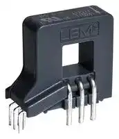
HO 25-NP/SP33-1000
Current Transducer, HO-NP Series, PCB, 25A, -62.5A to 62.5A, 1 %, Voltage Output, 3.3 Vdc
⚠️ Reference pricing provided. In case of supply shortages, we will connect you with our trusted procurement partners to ensure your project's continuity.
- Manufacturer: LEM
- Product type: Current Sensors
- Sensor Output:Voltage; Supply Voltage DC Min:3.14V; Supply Voltage DC Max:3.46V; Current Measuring Range DC:-62.5A to 62.5A; Current Measuring Range AC:-62.5A to 62.5A; Response Time
- SVHC: No SVHC (25-Jun-2025)
- Accuracy: ± 1%
- Accuracy %: 1%
- Product Range: HO-NP/SP33 Series
- Response Time: 3.5µs
- Primary Current: 25A
- Sensor Mounting: Through Hole
- Measured Current: AC / DC / Pulsed
- Sensor Output Type: Voltage
- Supply Voltage Range: 3.14V to 3.46V
- Secondary Signal Type: 1.65V
- Supply Voltage DC Max: 3.46V
- Supply Voltage DC Min: 3.14V
- Current Sensor Technology: Open Loop, Hall Effect
- Operating Temperature Max: 105°C
- Operating Temperature Min: -40°C
- Current Measuring Range AC: -62.5A to 62.5A
- Current Measuring Range DC: -62.5A to 62.5A
| Delivery and price | |
|---|---|
| Units per pack | 50 |
| Price | 6.38 € |
| Current stock | 10+ |
| Lead time | 30 days |
Datasheet

**Current Transducer HO-NP/SP33 series**

_I_ **PN = 8, 15, 25 A**

## **Ref: HO 8-NP/SP33, HO 15-NP/SP33, HO 25-NP/SP33**

**For the electronic measurement of current: DC, AC, pulsed..., with galvanic separation between the primary and the secondary circuit.**

## **Features**

- ●Hall effect measuring principle

- ●Multirange current transducer through PCB pattern lay-out

- ●Galvanic separation between primary and secondary circuit

- ●Insulated test voltage 4300 V

- ●Low power consumption

- ●Extremely low profile 12 mm

- ●Fixed offset & sensitivity

- ●Over-current detect 2.63 × _I_ PN (peak value)

- ●Memory check.

## **Applications**

- ●AC variable speed drives

- ●Static converters for DC motor drives

- ●Battery supplied applications

- ●Uninterruptible Power Supplies (UPS)

- ●Switched Mode Power Supplies (SMPS)

- ●Power supplies for welding applications

- ●The solar inverter on DC side of the inverter (MPPT)

- ●Combiner box.

## **Standards**

- ●EN 50178: 1997

## **Special feature**

- ●Single power supply +3.3 V.

## **Advantages**

- ●Small size and space saving

- ●Only one design for wide primary current range

- ●IEC 61010-1: 2010

- ●IEC 61326-1: 2012

- ●UL 508: 2010.

## **Application Domain**

   - ●Industrial.

- ●High immunity to external interference

- ●8 mm creepage /clearance

- ●Fast response.

N°74.50.11.033.0, N°74.50.15.033.0, N°74.50.19.033.0 21October2014/Version 4 LEM reserves the right to carry out modifications on its transducers, in order to improve them, without prior notice

Page 1/16

www.lem.com

**HO-NP/SP33 series**

## **Absolute maximum ratings**

**==> picture [512 x 19] intentionally omitted <==**

**----- Start of picture text -----**<br>
Parameter Symbol Unit Value<br>**----- End of picture text -----**<br>


|**Parameter**|**Symbol**|**Unit**|**Value**|
|---|---|---|---|
|||||
|Supply voltage (not operating)|_U_C|V|6.5|
|Primary conductor temperature|_T_B|°C|120|
|ESD rating, Human Body Model (HBM)|_U_ESD|kV|2|


Stresses above these ratings may cause permanent damage. Exposure to absolute maximum ratings for extended periods may degrade reliability.

## **UL 508: Ratings and assumptions of certification**

File # E189713 Volume: 2 Section: 5

## **Standards**

- CSA C22.2 NO. 14-10 INDUSTRIAL CONTROL EQUIPMENT - Edition 11 - Revision Date 2011/08/01

- UL  508 STANDARD FOR INDUSTRIAL CONTROL EQUIPMENT - Edition 17 - Revision Date 2010/04/15

## **Ratings**

**==> picture [512 x 19] intentionally omitted <==**

**----- Start of picture text -----**<br>
Parameter Symbol Unit Value<br>**----- End of picture text -----**<br>


|**Parameter**|**Symbol**|**Unit**|**Value**|
|---|---|---|---|
|||||
|Primary involved potential||V AC/DC|600|
|Max surrounding air temperature|_T_A|°C|105|
|Primary current|_I_P|A|According to series primary<br>currents|
|Secondary supply voltage|_U_C|V DC|3.3|
|Output voltage|_V_out|V|0 to 3.3|


## **Conditions of acceptability**

When installed in the end-use equipment, consideration shall be given to the following:

- _1 - These devices have been evaluated for overvoltage category III and for use in pollution degree 2 environment._

- _2 -  A suitable enclosure shall be provided in the end-use application._

- _3 - The terminals have not been evaluated for field wiring._

- _4 - These devices have been evaluated for use in 105 °C maximum surrounding air temperature._

- _5 -  The secondary (Sensing) circuit is intended to be supplied by a Isolated Secondary Circuit - Limited voltage circuit defined by UL 508 paragraph 32.5. The maximum open circuit voltage potential available to the circuit and overcurrent protection shall be evaluated in the end use application._

- _6 -  These devices are intended to be mounted on a printed wiring board of end-use equipment. The suitability of the connections (including spacings) shall be determined in the end-use application._

- _7 -  Primary terminals shall not be straightened since assembly of housing case depends upon bending of the terminals._

- _8 - Any surface of polymeric housing have not been evaluated as insulating barrier._

- _9 - Low voltage circuits are intended to be powered by a circuit derived from an isolating source (such as a transformer, optical isolator, limiting impedance or electro-mechanical relay) and having no direct connection back to the primary circuit (other than through the grounding means)._

## **Marking**

Only those products bearing the UL or UR Mark should be considered to be Listed or Recognized and covered under UL's Follow-Up Service. Always look for the Mark on the product.

Page 2/16 www.lem.com

LEM reserves the right to carry out modifications on its transducers, in order to improve them, without prior notice

21October2014/Version 4

**HO-NP/SP33 series**

## **Insulation coordination**

**==> picture [512 x 20] intentionally omitted <==**

**----- Start of picture text -----**<br>
Parameter Symbol Unit Value Comment<br>**----- End of picture text -----**<br>


|**Parameter**|**Symbol**|**Unit**|**Value**|**Comment**|
|---|---|---|---|---|
||||||
|Rms voltage for AC isolation test 50/60 Hz/1 min|_U_d|kV|4.3||
|Impulse withstand voltage 1.2/50 µs|_ÛW_|kV|8||
|Partial discharge extinction rms voltage @ 10 pC|_U_e|V|1650||
|Clearance (pri. - sec.)|_d_CI|mm|8|Shortest distance through air|
|Creepage distance (pri. - sec.)|_d_Cp|mm|8|Shortest path along device<br>body|
|Case material|||V0 according<br>to UL 94||
|Comparative tracking index|_CTI_||600||
|Application example|-|-|600 V<br>CAT III PD2|Reinforced insulation, non<br>uniform feld according to<br>EN 50178|
|Application example|-|-|300 V<br>CAT III PD2|Reinforced insulation, non<br>uniform feld according to<br>IEC 61010|
|Application example|-|-|1000 V<br>CAT III PD2|Simple insulation, non uniform<br>feld according to<br>EN 50178, IEC 61010|


## **Environmental and mechanical characteristics**

**==> picture [512 x 19] intentionally omitted <==**

**----- Start of picture text -----**<br>
Parameter Symbol Unit Min Typ Max Comment<br>**----- End of picture text -----**<br>


|**Parameter**|**Symbol**|**Unit**|**Min**|**Typ**|**Max**|**Comment**|
|---|---|---|---|---|---|---|
||||||||
|Ambient operating temperature|_T_A|°C|-40||105||
|Ambient storage temperature|_T_S|°C|-40||105||
|Surrounding temperature according to UL 508||°C|||105||
|Mass|_m_|g||5|||


Page 3/16

LEM reserves the right to carry out modifications on its transducers, in order to improve them, without prior notice

21October2014/Version 4

www.lem.com

**HO-NP/SP33 series**

## **Electrical data HO 8-NP/SP33-1000**

At _T_ A = 25 °C, _U_ C = +3.3 V, _N_ P = 3 turns, _R_ L = 10 KΩ unless otherwise noted (see Min, Max, typ. definition paragraph in page 12).

**==> picture [512 x 18] intentionally omitted <==**

**----- Start of picture text -----**<br>
Parameter Symbol Unit Min Typ Max Comment<br>**----- End of picture text -----**<br>


|**Parameter**|**Symbol**|**Unit**|**Min**|**Typ**|**Max**|**Comment**|
|---|---|---|---|---|---|---|
||||||||
|Primary nominal rms current|_I_**PN**|At||8|||
|Primary current, measuring range|_I_PM|At|-20||20||
|Number of primary turns|_N_P|||1,2,3|||
|Supply voltage|_U_C|V|3.14|3.3|3.46||
|Current consumption|_I_C|mA|||25||
|Reference voltage|_V_ref|V|1.636|1.65|1.664|Internal reference|
|External reference voltage|_V_ref|V|0.5||1.85|@_U_C= 3.3 ≈ 3.46 V|
||||0.5||1.7|@_U_C= 3.14 ≈ 3.3 V|
|Output voltage range @_I_PM|_V_out-_V_ref|V|-1.15||1.15||
|Output voltage @_I_P= 0 A|_V_out|V||_V_ref+_V_OE|||
|Electrical offset voltage|_V_OE|mV|-7||7||
|Temperature coeffcient of_V_ref|_TCV_ref|ppm/K|||±170|-20 °C .. 85 °C<br>Internal reference|
||||||±180|-40 °C .. 105 °C<br>Internal reference|
|Temperature coeffcient of_V_OE|_TCV_OE|mV/K|||±0.080|-40 °C .. 105 °C|
|Theoretical sensitivity|_G_th|mV/A||57.5||460 mV/_I_PN<br> @_U_C= 3.3 V|
|Sensitivity error|_εG_|%|||±0.5|Factory adjustment|
|Temperature coeffcient of_G_|_TCG_|ppm/K|||±200|-20 °C .. 85 °C|
||||||±210|-40 °C .. 105 °C|
|Linearity error 0 .._I_PN|_ε_L|% of_I_PN|||±0.5|@_U_C= 3.3 V|
|Linearity error 0 .._I_PM|_ε_L|% of_I_PM|||±0.8|@_U_C= 3.3 V|
|Gain error with respect to_U_C±10 %||%/%|||±0.4|Gain error per_U_Cdrift|
|Magnetic offset voltage<br>@_I_P= 0 after 2.5× _I_PN|_V_OM|mV|||±4||
|Reaction time @ 10 % of_I_PN|_t_ra|µs|||2|d_i_/d_t_=_I_PN/µs|
|Response time @ 90 % of_I_PN|_t_r|µs|||3.5|d_i_/d_t_=_I_PN/µs|
|Frequency bandwidth (-3 dB)|_BW_|kHz||250|||
|Output rms voltage noise (spectral density)<br>(DC .. 100 kHz)|_e_no|µV/√Hz|||18.9||
|Output voltage noise<br>(DC .. 20 MHz)|_V_no|mVpp||40|||
|Standby pin “0” level||V|||0.3||
|Standby pin “1” level||V|_U_C-0.3||||
|Time to switch from standby to normal mode||µs|||20||
|Over-current detect||At|2.6× _I_PN|2.9× _I_PN|3.2× _I_PN|peak value|
|Accuracy @_I_PN|_X_|% of_I_PN|||±1|=_ε_G+ _ε_L|
|Accuracy @_I_PN@_T_A= +85 °C|_X_|% of_I_PN|||±3.3|See formula note1)|
|Accuracy @_I_PN@_T_A= +105 °C|_X_|% of_I_PN|||±4.1|See formula note1)|


Note: 1) Accuracy @ _I_ P and _X_ TA = ± [ _X_ + ( _TCG_ /10000) · ( _T_ A - 25) + _TCV_ OE · 100 · ( _T_ A -25) / ( _G_ th · _I_ P)].

Page 4/16

LEM reserves the right to carry out modifications on its transducers, in order to improve them, without prior notice

21October2014/Version 4

www.lem.com

**HO-NP/SP33 series**

## **Electrical data HO 15-NP/SP33-1000**

At _T_ A = 25 °C, _U_ C = +3.3 V, _N_ P = 3 turns, _R_ L = 10 KΩ unless otherwise noted (see Min, Max, typ. definition paragraph in page 12).

**==> picture [512 x 18] intentionally omitted <==**

**----- Start of picture text -----**<br>
Parameter Symbol Unit Min Typ Max Comment<br>**----- End of picture text -----**<br>


|**Parameter**|**Symbol**|**Unit**|**Min**|**Typ**|**Max**|**Comment**|
|---|---|---|---|---|---|---|
||||||||
|Primary nominal rms current|_I_PN|At||15|||
|Primary current, measuring range|_I_PM|At|-37.5||37.5||
|Number of primary turns|_N_P|||1,2,3|||
|Supply voltage|_U_C|V|3.14|3.3|3.46||
|Current consumption|_I_C|mA|||25||
|Reference voltage|_V_ref|V|1.636|1.65|1.664|Internal reference|
|External reference voltage|_V_ref|V|0.5||1.85|@_U_C= 3.3 ≈ 3.46 V|
||||0.5||1.7|@_U_C= 3.14 ≈ 3.3 V|
|Output voltage range @_I_PM|_V_out-_V_ref|V|-1.15||1.15||
|Output voltage @_I_P= 0 A|_V_out|V||_V_ref+_V_OE|||
|Electrical offset voltage|_V_OE|mV|-5||5||
|Temperature coeffcient of_V_ref|_TCV_ref|ppm/K|||±170|-20 °C .. 85 °C<br>Internal reference|
||||||±180|-40 °C .. 105 °C<br>Internal reference|
|Temperature coeffcient of_V_OE|_TCV_OE|mV/K|||±0.080|-40 °C .. 105 °C|
|Theoretical sensitivity|_G_th|mV/A||30.67||460 mV/_I_PN, @_U_C= 3.3 V|
|Sensitivity error|_εG_|%|||±0.5|Factory adjustment|
|Temperature coeffcient of_G_|_TCG_|ppm/K|||±200|-20 °C .. 85 °C|
||||||±210|-40 °C .. 105 °C|
|Linearity error 0 .._I_PN|_ε_L|% of_I_PN|||±0.5|@_U_C= 3.3 V|
|Linearity error 0 .._I_PM|_ε_L|% of_I_PM|||±0.8|@_U_C= 3.3 V|
|Gain error with respect to_U_C±10 %||%/%|||±0.4|Gain error per_U_Cdrift|
|Magnetic offset voltage<br>@_I_P= 0 after 2.5× _I_PN|_V_OM|mV|||±4||
|Reaction time @ 10 % of_I_PN|_t_ra|µs|||2|d_i_/d_t_=_I_PN/µs|
|Response time @ 90 % of_I_PN|_t_r|µs|||3.5|d_i_/d_t_=_I_PN/µs|
|Frequency bandwidth (-3 dB)|_BW_|kHz||250|||
|Output rms voltage noise (spectral density)<br>(DC .. 100 MHz)|_e_no|µV/√Hz|||10.15||
|Output voltage noise<br>(DC .. 20 MHz)|_V_no|mVpp||30|||
|Standby pin “0” level||V|||0.3||
|Standby pin “1” level||V|_U_C-0.3||||
|Time to switch from standby to normal mode||µs|||20||
|Over-current detect||At|2.6× _I_PN|2.9× _I_PN|3.2× _I_PN|peak value|
|Accuracy @_I_PN|_X_|% of_I_PN|||±1|=_ε_G+ _ε_L|
|Accuracy @_I_PN@_T_A= +85 °C|_X_|% of_I_PN|||±3.3|See formula note1)|
|Accuracy @_I_PN@_T_A= +105 °C|_X_|% of_I_PN|||±4.1|See formula note1)|


Note: 1) Accuracy @ _I_ P and _X_ TA = ±  [ _X_ + ( _TCG_ /10000) · ( _T_ A - 25) + _TCV_ OE · 100 · ( _T_ A -25) / ( _G_ th · _I_ P)].

Page 5/16

LEM reserves the right to carry out modifications on its transducers, in order to improve them, without prior notice

21October2014/Version 4

www.lem.com

**HO-NP/SP33 series**

## **Electrical data HO 25-NP/SP33-1000**

At _T_ A = 25 °C, _U_ C = +3.3 V, _N_ P = 3 turns, _R_ L = 10 KΩ unless otherwise noted (see Min, Max, typ. definition paragraph in page 12).

**==> picture [513 x 21] intentionally omitted <==**

**----- Start of picture text -----**<br>
Parameter Symbol Unit Min Typ Max Comment<br>**----- End of picture text -----**<br>


|**Parameter**|**Symbol**|**Unit**|**Min**|**Typ**|**Max**|**Comment**|
|---|---|---|---|---|---|---|
||||||||
|Primary nominal rms current|_I_PN|At||25|||
|Primary current, measuring range|_I_PM|At|-62.5||62.5||
|Number of primary turns|_N_P|||1,2,3|||
|Supply voltage|_U_C|V|3.14|3.3|3.46||
|Current consumption|_I_C|mA|||25||
|Reference voltage|_V_ref|V|1.636|1.65|1.664|Internal reference|
|External reference voltage|_V_ref|V|0.5||1.85|@_U_C= 3.3 ≈ 3.46 V|
||||0.5||1.7|@_U_C= 3.14 ≈ 3.3 V|
|Output voltage range @_I_PM|_V_out-_V_ref|V|-1.15||1.15||
|Output voltage @_I_P= 0 A|_V_out|V||_V_ref+_V_OE|||
|Electrical offset voltage|_V_OE|mV|-6||6||
|Temperature coeffcient of_V_ref|_TCV_ref|ppm/K|||±170|-20 °C .. 85 °C<br>Internal reference|
||||||±180|-40 °C .. 105 °C<br>Internal reference|
|Temperature coeffcient of_V_OE|_TCV_OE|mV/K|||±0.080|-40 °C .. 105 °C|
|Theoretical sensitivity|_G_th|mV/A||18.4||460 mV/_I_PN@_U_C= 3.3 V|
|Sensitivity error|_εG_|%|||±0.5|Factory adjustment|
|Temperature coeffcient of_G_|_TCG_|ppm/K|||±200|-20 °C .. 85 °C|
||||||±210|-40 °C .. 105 °C|
|Linearity error 0 .._I_PN|_ε_L|% of_I_PN|||±0.5|@_U_C= 3.3 V|
|Linearity error 0 .._I_PM|_ε_L|% of_I_PM|||±0.8|@_U_C= 3.3 V|
|Gain error with respect to_U_C±10 %||%/%|||±0.4|Gain error per_U_Cdrift|
|Magnetic offset voltage<br>@_I_P= 0 after 2.5× _I_PN|_V_OM|mV|||±4||
|Reaction time @ 10 % of_I_PN|_t_ra|µs|||2|d_i_/d_t_=_I_PN/µs|
|Response time @ 90 % of_I_PN|_t_r|µs|||3.5|d_i_/d_t_=_I_PN/µs|
|Frequency bandwidth (-3 dB)|_BW_|kHz||250|||
|Output rms voltage noise (spectral density)<br>(DC .. 100 MHz)|_e_no|µV/√Hz|||6.13||
|Output voltage noise<br>(DC .. 20 MHz)|_V_no|mVpp||20|||
|Standby pin “0” level||V|||0.3||
|Standby pin “1” level||V|_U_C-0.3||||
|Time to switch from standby to normal mode||µs|||20||
|Over-current detect||At|2.6× _I_PN|2.9× _I_PN|3.2× _I_PN|peak value|
|Accuracy @_I_PN|_X_|% of_I_PN|||±1|=_ε_G+ _ε_L|
|Accuracy @_I_PN@_T_A= +85 °C|_X_|% of_I_PN|||±3.3|See formula note1)|
|Accuracy @_I_PN@_T_A= +105 °C|_X_|% of_I_PN|||±4.1|See formula note1)|


Note: 1) Accuracy @ _I_ P and _X_ TA = ± [ _X_ + ( _TCG_ /10000) · ( _T_ A - 25) + _TCV_ OE · 100 · ( _T_ A -25) / ( _G_ th · _I_ P)].

Page 6/16 www.lem.com

LEM reserves the right to carry out modifications on its transducers, in order to improve them, without prior notice

21October2014/Version 4

**HO-NP/SP33 series**

## **Typical performance characteristics** _I_ PN **= 8 A**

**==> picture [216 x 136] intentionally omitted <==**

**----- Start of picture text -----**<br>
Linearity error HO 8-NP/SP33<br>0.5<br>0.4<br>0.3<br>0.2<br>0.1<br>0<br>-0.1<br>-0.2<br>-0.3<br>-0.4<br>-0.5<br>-10 -8 -6 -4 -2 0 2 4 6 8 10<br>Primary current (A)<br>Linearity error (%)<br>**----- End of picture text -----**<br>


## _Figure 1: Linearity error_

**==> picture [250 x 133] intentionally omitted <==**

**----- Start of picture text -----**<br>
Frequency characteristics<br>Gain [0 dB at 50 Hz] Spec Phase<br>6.0 180<br>4.0 120<br>2.0 TITLE LETT 60<br>0.0 0<br>-2.0 -60<br>-4.0 -120<br>-6.0 -180<br>10 100 1000 10000 100000 1000000<br>Frequency [Hz]<br>Phase [deg]<br>Gain [0 dB at 50 Hz]<br>**----- End of picture text -----**<br>


## _Figure 2: Frequency response_

**==> picture [12 x 13] intentionally omitted <==**

**----- Start of picture text -----**<br>
Vout<br>Ip<br>**----- End of picture text -----**<br>


**==> picture [136 x 121] intentionally omitted <==**

**----- Start of picture text -----**<br>
Vout<br>| Ip<br>a I ea<br> es ns SUrs<br>P4-- PS. -- PG: -- P7---<br>11.6%v : :<br>2 µs/div (Timebase20.0k8 2.00-4.00 us1.0usidiv]68/s}Edge(TriggerStop _<br>**----- End of picture text -----**<br>


**==> picture [33 x 9] intentionally omitted <==**

**----- Start of picture text -----**<br>
1 µs/div<br>**----- End of picture text -----**<br>


**==> picture [99 x 9] intentionally omitted <==**

**----- Start of picture text -----**<br>
Figure 3: Step response<br>**----- End of picture text -----**<br>


_Figure 4: dv/dt_

**==> picture [41 x 8] intentionally omitted <==**

**----- Start of picture text -----**<br>
20 mV/div<br>**----- End of picture text -----**<br>


**==> picture [90 x 9] intentionally omitted <==**

**----- Start of picture text -----**<br>
Figure 5: Output noise<br>**----- End of picture text -----**<br>


Page 7/16

LEM reserves the right to carry out modifications on its transducers, in order to improve them, without prior notice

21October2014/Version 4

www.lem.com

**HO-NP/SP33 series**

## **Typical performance characteristics** _I_ PN **= 15 A**

**==> picture [496 x 137] intentionally omitted <==**

**----- Start of picture text -----**<br>
Linearity error HO 15-NP/SP33<br>Frequency characteristics<br>0.5<br>Gain [0 dB at 50 Hz] Spec Phase<br>0.4<br>6.0 180<br>0.3<br>0.2 4.0 120<br>0.1 2.0 60<br>0<br>-0.1 0.0 0<br>-0.2 -2.0 -60<br>-0.3<br>-4.0 -120<br>-0.4<br>-0.5 -6.0 -180<br>-20 -15 -10 -5 0 5 10 15 20 10 100 1000 10000 100000 1000000<br>Primary current (A) Frequency [Hz]<br>Linearity error (%)<br>Phase [deg]<br>Gain [0 dB at 50 Hz]<br>**----- End of picture text -----**<br>


_Figure 6: Linearity error_

## _Figure 7: Frequency response_

**==> picture [124 x 128] intentionally omitted <==**

**----- Start of picture text -----**<br>
\ aa| it r Vout r<br>ee\\est Ip<br>\ —<br>| +<br>SE errr<br>| T<br>P4--- PS--- PB-- PT---<br>9.2%v<br>imebase -4.00<br>2.00 usidiv]9)(TiggerStop<br>20.08 1.06Sis|Edge<br>2 µs/div Xi=X2= 2.788Ons ys 1iAX=X=<br>**----- End of picture text -----**<br>


**==> picture [32 x 9] intentionally omitted <==**

**----- Start of picture text -----**<br>
1 µs/div<br>**----- End of picture text -----**<br>


**==> picture [12 x 13] intentionally omitted <==**

**----- Start of picture text -----**<br>
Vout<br>Ip<br>**----- End of picture text -----**<br>


**==> picture [99 x 10] intentionally omitted <==**

**----- Start of picture text -----**<br>
Figure 8: Step response<br>**----- End of picture text -----**<br>


**==> picture [59 x 10] intentionally omitted <==**

**----- Start of picture text -----**<br>
Figure 9: dv/dt<br>**----- End of picture text -----**<br>


**==> picture [41 x 8] intentionally omitted <==**

**----- Start of picture text -----**<br>
20 mV/div<br>**----- End of picture text -----**<br>


**==> picture [95 x 9] intentionally omitted <==**

**----- Start of picture text -----**<br>
Figure 10: Output noise<br>**----- End of picture text -----**<br>


Page 8/16

LEM reserves the right to carry out modifications on its transducers, in order to improve them, without prior notice

21October2014/Version 4

www.lem.com

**HO-NP/SP33 series**

## **Typical performance characteristics** _I_ PN **= 25 A**

**==> picture [217 x 136] intentionally omitted <==**

**----- Start of picture text -----**<br>
Linearity error HO 25-NP/SP33<br>0.5<br>0.4<br>0.3<br>0.2<br>0.1<br>0<br>-0.1<br>-0.2<br>-0.3<br>-0.4<br>-0.5<br>-30 -20 -10 0 10 20 30<br>Primary current (A)<br>Linearity error (%)<br>**----- End of picture text -----**<br>


**==> picture [250 x 134] intentionally omitted <==**

**----- Start of picture text -----**<br>
Frequency characteristics<br>Gain [0 dB at 50 Hz] Spec Phase<br>6.0 180<br>4.0 120<br>2.0 60<br>0.0 0<br>-2.0 -60<br>-4.0 -120<br>-6.0 -180<br>10 100 1000 10000 100000 1000000<br>Frequency [Hz]<br>Phase [deg]<br>Gain [0 dB at 50 Hz]<br>**----- End of picture text -----**<br>


## _Figure 11: Linearity error_

## _Figure 12: Frequency response_

**==> picture [12 x 13] intentionally omitted <==**

**----- Start of picture text -----**<br>
Vout<br>Ip<br>**----- End of picture text -----**<br>


**==> picture [12 x 14] intentionally omitted <==**

**----- Start of picture text -----**<br>
Vout<br>Ip<br>**----- End of picture text -----**<br>


**==> picture [237 x 234] intentionally omitted <==**

**----- Start of picture text -----**<br>
Li mv}Etali -230.0 mV|_| 2 µs/div 20.0kSx1=X= 2799sOns1.0 GSis}EdgeMAXAX 357.32.799ys KHZNegative}<br>Figure 13: Step response<br>20 mV/div<br>pO Oe<br>rs rr<br>oe<br>PAspkpk(C2)21 mvv P2:max(C2)—-11.5 mVv P3:min(C2)“8.7 mvv Pa P5--- P6:---imebase -100ms|(TriagerPT---<br>0.0020.0 mVmVidivofst| 1008 60.0msidivfStop200kS/s[Edge<br>Figure 15: Output noise<br>**----- End of picture text -----**<br>


**==> picture [64 x 9] intentionally omitted <==**

**----- Start of picture text -----**<br>
Figure 14: dv/dt<br>**----- End of picture text -----**<br>


**==> picture [32 x 9] intentionally omitted <==**

**----- Start of picture text -----**<br>
1 µs/div<br>**----- End of picture text -----**<br>


Page 9/16

LEM reserves the right to carry out modifications on its transducers, in order to improve them, without prior notice

21October2014/Version 4

www.lem.com

**HO-NP/SP33 series**

## **Maximum continuous DC primary primary current**

**==> picture [511 x 219] intentionally omitted <==**

**----- Start of picture text -----**<br>
50 100<br>40<br>75<br>30<br>50<br>20<br>25<br>10<br>15A8A 15A15A<br>0 0<br>0 25 50 75 100 125 0 25 50 75 100 125<br>T A( ℃ ) T A( ℃ )<br>I  (A)p I  (A)p<br>**----- End of picture text -----**<br>


**==> picture [216 x 218] intentionally omitted <==**

**----- Start of picture text -----**<br>
125<br>100<br>75<br>50<br>25<br>25A<br>0<br>0 25 50 75 100 125<br>T A( ℃ )<br> (A)<br>p<br>I<br>**----- End of picture text -----**<br>


_Figure 16: IP vs TA for HO series_

Important notice:  whatever the usage and/or application, the transducer jumper temperature shall not go above the maximum rating of 120 °C as stated in page 2 of this datasheet.

Page 10/16 www.lem.com

LEM reserves the right to carry out modifications on its transducers, in order to improve them, without prior notice

21October2014/Version 4

**HO-NP/SP33 series**

## **Measuring range with external reference voltage**

**==> picture [465 x 469] intentionally omitted <==**

**----- Start of picture text -----**<br>
50<br>40 Upper limit: IP = 17.39  ×  Vref  +48.7 (Vref   = 0.5 .. 1.65 V)<br>30<br>20 Lower limit: IP = 17.39  ×  Vref  +8.7 (Vref   = 0.5 .. 1.65 V)<br>10<br>0<br>-10<br>-20<br>HO 8<br>-30<br>0.5 1 1.5<br>V ref (V)<br>100<br>80<br>60 Upper limit: IP = -32.81  ×  Vref  +91.3 (Vref   = 0.5 .. 1.65 V)<br>40<br>20 Lower limit: IP = -32.81  ×  Vref  +16.3 (Vref   = 0.5 .. 1.65 V)<br>0<br>-20<br>-40<br>HO 15<br>-60<br>0.5 1 1.5<br>V ref (V)<br>120<br>Upper limit:<br>90 TA = 105 °C  IP = 80 (Vref   = 0.5..1.328 V)<br>60 IP = -54.35 × Vref  +152.17 (Vref   = 1.328 .. 1.65 V)<br>25 ℃<br>30 60 ℃ TA = 85 °C  IP = 90 (Vref   = 0.5..1.144 V)<br>0 85 ℃ IP = -54.35 × Vref  +152.17 (Vref   = 1.144 .. 1.65 V)<br>-30 105 ℃ TA = 80 °C  IP = 100 (Vref   = 0.5..0.96 V)<br>IP = -54.35 × Vref  +152.17 (Vref   = 0.96 .. 1.65 V)<br>-60<br>HO 25<br>-90 TA = 25 °C  IP = 110 (Vref   = 0.5..0.776 V)<br>0.5 1 1.5 IP = -54.35 × Vref  +152.17 (Vref   = 0.776 .. 1.65 V)<br>V ref (V) Lower limit:  IP = -54.35 × Vref  +27.17 (Vref   = 0.5 .. 1.65 V)<br> (A)<br>p<br>I<br> (A)<br>p<br>I<br> (A)<br>p<br>I<br>**----- End of picture text -----**<br>


_Example with Vref  = 0.5 V:_

- ●The 8 A version has a measuring range from 0 A to 40 A

- ●The 15 A version has a measuring range from 0 A to 75 A

- ●The 25 A version has a measuring range from 0 A to 80 A at _TA_ = 105 °C _Example with Vref  = 1.5 V:_

- ●The 8 A version has a measuring range from -17.4 A to 22.6 A

- ●The 15 A version has a measuring range from -32.6 A to +42.4 A

- ●The 25 A version has a measuring range from -54.4 A to +70.6 A

Page 11/16

21October2014/Version 4 LEM reserves the right to carry out modifications on its transducers, in order to improve them, without prior notice

www.lem.com

**HO-NP/SP33 series**

## **Application information**

## **Total primary resistance**

The primary resistance is 0.36 mΩ per conductor at 25 °C.

In the following table, examples of primary resistance according to the number of primary turns.

|Number of<br>primary turns|Primary resistance<br>current rms<br>_R_P[ mΩ ]|Recommended connections|Primary nominal current<br>_I_PN[ A ]|Primary nominal current<br>_I_PN[ A ]|Primary nominal current<br>_I_PN[ A ]|
|---|---|---|---|---|---|
|1|0.12|13      12       11        OUT<br>IN8 910|8|15|25|
|2|0.54|13      12      11        OUT<br>IN         8        9       10|4|7.5|12.5|
|3|1.18|13      12      11        OUT<br>IN        8        9        10|2.67|5|8.33|


## **Definition of typical, minimum and maximum values**

Minimum and maximum values for specified limiting and safety conditions have to be understood as such as well as values shown in “typical” graphs. On the other hand, measured values are part of a statistical distribution that can be specified by an interval with upper and lower limits and a probability for measured values to lie within this interval.

Unless otherwise stated (e.g. “100 % tested”), the LEM definition for such intervals designated with “min” and “max” is that the probability for values of samples to lie in this interval is 99.73 %. For a normal (Gaussian) distribution, this corresponds to an interval between -3 sigma and +3 sigma. If “typical” values are not obviously mean or average values, those values are defined to delimit intervals with a probability of 68.27 %, corresponding to an interval between -sigma and +sigma for a normal distribution.

Typical, maximal and minimal values are determined during the initial characterization of a product.

## **Remark**

Installation of the transducer must be done unless otherwise specified on the datasheet, according to LEM Transducer Generic Mounting Rules. Please refer to LEM document N°ANE120504 available on our Web site: **Products/Product Documentation.**

Page 12/16 www.lem.com

LEM reserves the right to carry out modifications on its transducers, in order to improve them, without prior notice

21October2014/Version 4

**HO-NP/SP33 series**

## **HO-NP/SP33 Series: name and codification**

HO family products may be ordered _**on request**_ 1) with a dedicated setting of the parameters described below (standards products are delivered with the setting 0000 according to the table).

## **HO 15-NP/SP33-XXXX**

**==> picture [478 x 212] intentionally omitted <==**

**----- Start of picture text -----**<br>
|||||||||
|---|---|---|---|---|---|---|---|
|Reference out:|Response time:|EEPROM Control:|Over current detection:|
|0|2.5 V|0|3.5 µs|0|YES|0|2.9|
|1|1.65 V|1|2 µs|1|NO|1|3.6|
|2|1.5 V|2|6 µs|2|4.0|
|3|0.5 V|3|4.8|SET_THRESH = 0|
|4|only|V|ref IN|4|5.2|
|(Low power mode engaged)|5|5.8|
|6|1.7|
|7|2.3|
|A|0.67|
|B|0.94|
|C|1.17|
|D|1.4|
|SET_THRESH = 1|
|E|1.6|
|F|1.9|
|G|2.1|
|H|2.3|
|:|

**----- End of picture text -----**<br>


The products of this datasheet are the following references:

- HO 8-NP/SP33-1000

- HO 15-NP/SP33-1000

- HO 25-NP/SP33-1000

Note:[1)] For other dedicated settings, minimum quantities apply.

Page 13/16

LEM reserves the right to carry out modifications on its transducers, in order to improve them, without prior notice

21October2014/Version 4

www.lem.com

**HO-NP/SP33 series**

## **PCB Footprint**

## **Assembly on PCB**

- Recommended PCB hole diameter

   - 1.5 mm for primary pin

   - 0.9 mm for secondary pin

- Maximum PCB thickness

- Wave soldering profile No clean process only

- 2.4 mm

- maximum 260 °C, 10 s

## **Safety**

This transducer must be used in limited-energy secondary circuits according to IEC 61010-1.

This transducer must be used in electric/electronic equipment with respect to applicable standards and safety requirements in accordance with the manufacturer’s operating instructions.

## Caution, risk of electrical shock.

When operating the transducer, certain parts of the module can carry hazardous voltage (e.g. primary bus bar, power supply). Ignoring this warning can lead to injury and/or cause serious damage.

This transducer is a build-in device, whose conducting parts must be inaccessible after installation.

A protective housing or additional shield could be used.

Main supply must be able to be disconnected.

Page 14/16 www.lem.com

LEM reserves the right to carry out modifications on its transducers, in order to improve them, without prior notice

21October2014/Version 4

**HO-NP/SP33 series**

## **Performance parameters definition**

## **Ampere-turns and amperes**

The transducer is sensitive to the primary current linkage ΘP (also called ampere-turns).

- ΘP = _N_ P· _I_ P (At)

- Where _N_ P is the number of primary turn (depending on the connection of the primary jumpers)

Caution: As most applications will use the transducer with only one single primary turn ( _N_ P = 1), much of this datasheet is written in terms of primary current instead of current linkages. However, the ampere-turns (At) unit is used to emphasis that current linkages are intended and applicable.

## **Transducer simplified model**

The static model of the transducer at temperature _T_ A is: _V_ out = _G_ ·ΘP + overall error (mV) In which error =

_εG_ ·ΘP· _G_ + _ε_ L·ΘP· _G_ + _TCG_ ( _T_ A-25)·ΘP· _G + V_ OE + _TCV_ OE·( _T_ A-25) (mV)

With: ΘP = _N_ P· _I_ P :  primary current linkage (At) ΘP max :  max primary current linkage applied to the transducer (At) _V_ out : output voltage (V) _T_ A : ambient operating temperature (°C) _VOE_ : electrical offset current (V) _TCV_ OE : temperature coefficient of _V_ OE (mV/K) _G_ : sensitivity of the transducer (V/At) _TCG_ : temperature coefficient of _G (%/K) εG_ : sensitivity error (%) _ε_ L(ΘP max) : linearity error for ΘP max (%)

This model is valid for primary ampere-turns ΘP between -ΘP max and +ΘP max only.

## **Sensitivity and linearity**

To measure sensitivity and linearity, the primary current (DC) is cycled from 0 to _I_ P, then to - _I_ P and back to 0 (equally spaced _I_ P/10 steps). The sensitivity _G_ is defined as the slope of the linear regression line for a cycle between ± _I_ PN.

The linearity error εL is the maximum positive or negative difference between the measured points and the linear regression line, expressed in % of _I_ PN.

## **Magnetic offset**

The magnetic offset voltage _V_ OM is the consequence of a current on the primary side (“memory effect” of the transducer’s ferromagnetic parts). It is measured using the following primary current cycle. _V_ OM depends on the current value _I_ P1 ( _I_ P1> _I_ PM).

**==> picture [96 x 24] intentionally omitted <==**

**==> picture [225 x 132] intentionally omitted <==**

**----- Start of picture text -----**<br>
I P [(DC) ]<br>I P1<br>t 2<br>0 A<br>                    t 1  t<br>- I P1<br>Figure 17:  Current cycle used to measure magnetic and<br>electrical offset<br>(transducer supplied)<br>**----- End of picture text -----**<br>


## **Electrical offset**

The electrical offset voltage _V_ OE can either be measured when the ferro-magnetic parts of the transducer are:

- ●completely demagnetized, which is difficult to realize,

- ●or in a known magnetization state, like in the current cycle shown in figure 17.

Using the current cycle shown in figure 18, the electrical offset is:

**==> picture [73 x 19] intentionally omitted <==**

Note: the transducer has to be demagnetized prior to the application of the current cycle (for example with a demagnetization tunnel).

## **Overall accuracy**

The overall accuracy at 25 °C _XG_ is the error in the - _I_ PN .. + _I_ PN  range, relative to the rated value _I_ PN. It includes:

- ●the electrical offset _V_ OE/ ΘP· _G_ (%)

- ●the sensitivity error _εG_ (%)

- ●the linearity error _ε_ L (to _I_ PN) (%)

## **Response and reaction times**

The response time figure 18 _t_ r and the reaction time _t_ ra are shown in

Both depend on the primary current d _i/_ d _t_ . They are measured at nominal ampere-turns.

**==> picture [170 x 119] intentionally omitted <==**

**----- Start of picture text -----**<br>
I<br>100 %<br>90 %<br>I p V out<br>t r<br>10 %<br>t ra t<br>**----- End of picture text -----**<br>


_Figure 18: Response time t_ r _and reaction time t_ ra

Page 15/16 www.lem.com

LEM reserves the right to carry out modifications on its transducers, in order to improve them, without prior notice

21October2014/Version 4

**HO-NP/SP33 series**

## **Dimensions HO 8-NP/SP33, HO 15-NP/SP33, HO 25-NP/SP3**

(mm, general linear tolerance ±0.5 mm)

**==> picture [512 x 480] intentionally omitted <==**

**----- Start of picture text -----**<br>
Required Connection<br>OUT<br>11 12 13<br>1<br>2 47nF + U c<br>0V<br>5 Ω 3 4.7nF<br>V out<br>200 Ω 4 47nF<br>5 >10kΩ V ref  (IN/OUT)<br>OCD<br>6<br>STANDBY<br>7<br>10 9 8 N/A (connected to ground)<br>IN<br>d CI d Cp<br>**----- End of picture text -----**<br>


Page 16/16

LEM reserves the right to carry out modifications on its transducers, in order to improve them, without prior notice

21October2014/Version 4

www.lem.com
Updated at June 10, 2026
About Novapart
Novapart is a B2B electronic component broker specialising in stock shortages and cost reduction. We source hard-to-find parts and identify compliant alternatives across a catalogue of 410,000+ components from 500+ manufacturers.
Learn more →Stock Shortage Specialist
When a component is unavailable, discontinued or has an unacceptable lead time, we tap into our network of vetted European and Asian distributors to source what you need — without compromising on quality or traceability.
Request a quote →Compliant Alternatives
We identify pin-to-pin, electrically equivalent substitutes that meet the same certifications (RoHS, AEC-Q100, REACH) as your original specification — validated against datasheets, not just part numbers. Often at a lower cost.
BOM Analysis service →