
Image not available
Illustrative purposes only


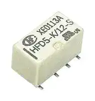
HFD5-K/5-SR
Signal Relay, 5 VDC, DPDT, 1 A, HFD5-K Series, Surface Mount, Non Latching
⚠️ Reference pricing provided. In case of supply shortages, we will connect you with our trusted procurement partners to ensure your project's continuity.
- Manufacturer: HONGFA
- Product type: Signal Relays
- SVHC: No SVHC (04-Feb-2026)
- Coil Type: Non Latching
- Coil Voltage: 5VDC
- Product Range: HFD5-K Series
- Relay Mounting: Surface Mount
- Coil Resistance: 179ohm
- Contact Current: 1A
- Relay Terminals: PC Pin
- Contact Material: Silver Alloy
- Contact Voltage VAC: -
- Contact Voltage VDC: 30V
- Contact Configuration: DPDT
| Delivery and price | |
|---|---|
| Units per pack | 100 |
| Price | 1.57 € |
| Current stock | 10+ |
| Lead time | 30 days |
Datasheet

## **HFD5-K**

## **MINIATURE 5TH GENERATION SIGNAL RELAY**

## **Features**

- An ideal alternative for small reed relays

- Operate/release (reset) time ≤ 1.0ms

- Bifurcated contacts

- 2 Form C configuration

- Products with electrical endurance ≥ 5x10[8] ops available

- Low halogen products conforming to IEC61249-2-21 are available

- Both THT & SMT types available

- Single side stable and latching type available

- Smallest size in signal relay industry: 9.0(L)×4.8(W)×4.9(H) mm

File No. : E133481

**RoHS compliant**

## **CHARACTERISTICS**

## **CONTACT DATA**

**==> picture [213 x 187] intentionally omitted <==**

**----- Start of picture text -----**<br>
||||||||||||
|---|---|---|---|---|---|---|---|---|---|---|
|Contact arrangement|2Z|
|Contact resistance|≤|100mΩ(10mA 30mVDC)|
|Contact material|Ag alloy+Au plated|
|Contact rating|0.5A 30VDC|||1A  30VDC|
|(Res. load)|0.3A 125VAC|
|Max. switching current|2A(30VDC)|
|Max. switching voltage|125VAC/60VDC|
|Max. switching power|37.5VA/30W|
|Min.  applicable load|[2)]|10mV 10μA|
|Mechanical endurance|5×10|[8]|次|
|1×10|[5]|OPS|
|(85|℃,|1s on|:|9soff|,|NOorNC|,|0.5A 30VDC)|
|Electrical|1×10|[5]|OPS|
|endurance|[3)]|(85|℃,|1s on|:|9s off|,|NO or NC|,|0.3A 125VAC)|
|3×10|[8]|OPS(AJ8)|[4)]|
|(40|℃,|0.1s on|:|0.1s off|,|
|Two sets of NO or NC in paralle|[5)]|,|
|10mA 5VDC)|

**----- End of picture text -----**<br>


**==> picture [231 x 220] intentionally omitted <==**

**----- Start of picture text -----**<br>
|||||||
|---|---|---|---|---|---|
|Insulation resistance|1000MΩ(500VDC)|
|Between open contacts|500VAC 1min|
|Dielectric|Between coil &|1000VAC 1min,|
|||strength|||contacts|1500VAC1min(413 specificationonly)|[2)]|
|Between contact|
|1000VAC 1min|
|sets|
|||
|Operate time (Set time)|≤|1.0ms|
|Release time (Reset time)|≤|1.0ms|
|Shock|Functional|735m/s|[2]|
|||
|resistance|Destructive|980m/s|[2]|
|||
|Vibration|Functional|10Hz~55Hz  3.3mm DA|
|resistance|Destructive|10Hz~55Hz  5.0mm DA|
||||
|Humidity|5% to 85%RH|
|Ambient temperature|-40|℃|to 85|℃|
|Termination|THT|SMT|
|Unit weight|Approx. 0.5g|
|Moisture sensitivity levels|
|(Only for SMT type,|MSL-3|
|JEDEC-STD-020)|
|Construction|Plastic sealed|

**----- End of picture text -----**<br>


**Notes:** 1)The data shown above are initial values.

- 2) Min. applicable load is reference value. Please perform the confirmation test with the actual load before production since reference value may change according to switching frequencies, environmental conditions and expected contact resistance and reliability.

**Notes:** 1) The data shown above are initial values ; 2) (413) indicates products with dielectric withstand voltage between coil and contact ≥ 1500VAC 1 min

- 3) Only typical loads are listed above. Other load specifications can be available upon request.

- 4) (AJ8) indicates products with electrical endurance ≥ 3x10[8] OPS .

- 5) Two sets of NO or NC parallel wiring diagrams (bottom view) are as follows:

**==> picture [421 x 73] intentionally omitted <==**

**----- Start of picture text -----**<br>
1 2 3 4 1 2 3 4 COIL<br>Single side stable   See table“COIL DATA”<br>8 7 6 5 8 7 6 5 Coil power 1 coil latching See table“COIL DATA”<br>Orientation mark Orientation mark<br>6) For low level and long durability applications, it is recommended  ——— Temperature rise ≤ 50K(0.5A Load,at 85 ℃ )<br>to use two sets of NO or NC in parallel. If you need to use a<br>single set of NO or NC, please contact our company.<br>**----- End of picture text -----**<br>


## **HIGH-FREQUENCY CHARACTERISTICS**[1)]

**==> picture [201 x 45] intentionally omitted <==**

**----- Start of picture text -----**<br>
|||||
|---|---|---|---|
|Frequency|[2)]|100MHz|900MHz|
|Insertion loss|[3)]|0.03dB|0.3dB|
|V.SWR|[3)]|1.05|1.4|
|Isolation|[3)]|45dB|25dB|

**----- End of picture text -----**<br>


**Notes:** 1)The characteristic impedance of the measuring system is 50Ω . 2)If there is a demand for frequencies higher than  1GHz,please contact us. 3)The data shown above are initial values .

**SAFETY APPROVAL RATINGS** 0.5A 30VDC UL/CUL Ag alloy+Au plated 1A 30VDC 0.3A 125VAC **Notes:** 1) Only some typical rating are listed above.If more details are required,please contact us.

## HONGFA RELAY

ISO9001, IATF16949 , ISO14001, ISO45001, IECQ QC 080000, ISO/IEC 27001 CERTIFIED

2025  Rev.2.00

001

23 ℃

## **COIL DATA**

## **Single side stable**

**==> picture [441 x 161] intentionally omitted <==**

**----- Start of picture text -----**<br>
Nominal Initial Pick-up Initial  Drop-out Coil Nominal Nominal Power Max.<br>Coil Code Voltage VoltageVDC [2)] VoltageVDC [1)] Resistance current mW Voltage<br>VDC max. max. Ω mA approx VDC [5)]<br>HFD5-K/1.5 1.5 1.13 0.15 16×(1±10%) 93 140 2.3<br>HFD5-K/2.4 2.4 1.80 0.24 41×(1±10%) 58 140 3.6<br>HFD5-K/3 [3)] 3.0 2.25 0.30 64.3×(1±10%) 47 140 4.5<br>HFD5-K/4.5 4.5 3.38 0.45 145×(1±10%) 31 140 6.8<br>HFD5-K/5 [3)] 5.0 3.75 0.50 179×(1±10%) 28 140 7.5<br>HFD5-K/6 6.0 4.50 0.60 257×(1±10%) 23 140 9.0<br>HFD5-K/9 9.0 6.75 0.90 579×(1±10%) 16 140 13.5<br>HFD5-K/12 12.0 9.00 1.20 1029×(1±10%) 12 140 18.0<br>HFD5-K/24 24.0 18.00 2.40 4114×(1±10%) 6 140 36.0<br>**----- End of picture text -----**<br>


## **1 coil latching**

**==> picture [441 x 159] intentionally omitted <==**

**----- Start of picture text -----**<br>
Nominal Initial Pick-up Initial  Drop-out Coil Nominal Nominal Power Max.<br>Coil Code Voltage VoltageVDC [2)] VoltageVDC [1)] Resistance current mW Voltage<br>VDC max. max. Ω mA approx VDC [5)]<br>HFD5-K/1.5-L 1.5 1.13 1.13 16×(1±10%) 93 140 2.3<br>HFD5-K/2.4-L 2.4 1.80 1.80 41×(1±10%) 58 140 3.6<br>HFD5-K/3-L [3)] 3.0 2.25 2.25 64.3×(1±10%) 47 140 4.5<br>HFD5-K/4.5-L 4.5 3.38 3.38 145×(1±10%) 31 140 6.8<br>HFD5-K/5-L [3)] 5.0 3.75 3.75 179×(1±10%) 28 140 7.5<br>HFD5-K/6-L 6.0 4.50 4.50 257×(1±10%) 23 140 9.0<br>HFD5-K/9-L 9.0 6.75 6.75 579×(1±10%) 16 140 13.5<br>HFD5-K/12-L 12.0 9.00 9.00 1029×(1±10%) 12 140 18.0<br>HFD5-K/24-L 24.0 18.00 18.00 4114×(1±10%) 6 140 36.0<br>**----- End of picture text -----**<br>


**Notes:** 1)The data shown above are initial values.

- 2)  Initial Pick-up voltage is the factory value of the relay

- To supply rated step voltage to coil is the foundation of relay proper operation. Please make sure the applied voltage to the coil reach at rated values.

Please refer to the typical diagram below for single side stable relay. The “V_coil” is the rated voltage. :

**==> picture [164 x 147] intentionally omitted <==**

**----- Start of picture text -----**<br>
VCC<br>RES2 V_coil<br>RELAY DIODE V<br>Port1<br>RES1<br>GND<br>**----- End of picture text -----**<br>


- 3) In case 5V of transistor drive circuit, it is recommended to use 4.5V type relay, and 3V to use 2.4V type relay.

- 4) For monostable relays , if you need to drop down voltage and hold mode after reliably operating,make sure that the effective value of holding voltage is not less than 60% of the rated voltage.

- 5) Maximum voltage refers to the maximum voltage which relay  coil could endure in a short period of time.

- 6) When user's requirements can't be found in the above table, special order allowed.

- 7) During the relay pick-up or drop-out processes, there are stages of contact pressure change, contact vibration and unstable contact etc. When the voltage applied to coil is gradually changed, it will lengthen the unstable stage and affect relay endurance. To reduce this influence, please apply step voltage(switching circuit) to relay coil.

002

## **ORDERING INFORMATION**

**==> picture [442 x 220] intentionally omitted <==**

**----- Start of picture text -----**<br>
HFD5-K/ 12 -L S R ( XXX )<br>Type<br>1.5 2.4 3 4.5<br>Coil voltage 5 6 9 12 24VDC<br>Sort L:  1 coil latching Nil:  Single side stable<br>S:  Standard SMT<br>Terminal type         S1:  Short terminal SMT<br>Nil:  THT [1)]<br>R:  Tape and reel packing (Only for SMT type) [2)]<br>Packing style Nil:  Tube packing(Only for THT type)<br>XXX:  Customer special requirement Nil:  Standard<br>For instance: Product with  825 suffix is applicable to low level load applications, such as<br>Special code testing, medical treament , communication, etc.<br>Product with AQ8 suffix is indicate electrical endurance ≥ 5x10 [8] OPS<br>Product with 413 suffix is indicale dielectric withstand voltage between coil<br>and conlact1500VAC 1 min.<br>**----- End of picture text -----**<br>


Notes: 1) Please use wave soldering or manual  soldering for straight-in relay.If you need reflow welding please confirm the feasibility with us.

- 2)  R type (tape and reel) packing is moisture-proof which meets requirement of MSL-3. Please choose R type packing for SMT products. For R type, the letter "R" will only be printed on packing tag but not on relay cover. Tube packing is normally not available for SMT products unless specially requested by customer. But please note that tube packing is not moisture-proof so please bake the products before use according to description of Notice 11 herewith. In addition, tube packaging will be adopted when the ordering quantity of R type is equal to or less than 100 pieces unless otherwise specified.

   - 3) When coil sort, terminal type or packing style are needed, pleaes add "-" after coil voltage is selected. For instance, HFD5-K/12-SR.

   - 4) The customer special requirement express as special code after evaluating by Hongfa.

## **OUTLINE DIMENSIONS, WIRING DIAGRAM AND PC BOARD LAYOUT**

**==> picture [24 x 6] intentionally omitted <==**

**----- Start of picture text -----**<br>
Unit: mm<br>**----- End of picture text -----**<br>


**==> picture [86 x 8] intentionally omitted <==**

**----- Start of picture text -----**<br>
Outline Dimensions<br>**----- End of picture text -----**<br>


**==> picture [100 x 10] intentionally omitted <==**

**----- Start of picture text -----**<br>
PCB Layout(Bottom view)<br>**----- End of picture text -----**<br>


THT

**==> picture [196 x 115] intentionally omitted <==**

**----- Start of picture text -----**<br>
9 4.8<br>0.7 0.4 0.15<br>3.2<br>3.2 2.2 2.2<br>**----- End of picture text -----**<br>


**==> picture [116 x 81] intentionally omitted <==**

**----- Start of picture text -----**<br>
3.2 2.2 2.2<br>8x   0.85<br>**----- End of picture text -----**<br>


## S type: Standard SMT

**==> picture [197 x 95] intentionally omitted <==**

**----- Start of picture text -----**<br>
9 4.8<br>0.7 0.4 0.15<br>3.2 2.2 2.2 3.2<br>5.7<br>**----- End of picture text -----**<br>


**==> picture [115 x 81] intentionally omitted <==**

**----- Start of picture text -----**<br>
3.2 2.2 2.2<br>0.8<br>**----- End of picture text -----**<br>


003

## **OUTLINE DIMENSIONS, WIRING DIAGRAM AND PC BOARD LAYOUT**

**==> picture [24 x 5] intentionally omitted <==**

**----- Start of picture text -----**<br>
Unit: mm<br>**----- End of picture text -----**<br>


**==> picture [85 x 8] intentionally omitted <==**

**----- Start of picture text -----**<br>
Outline Dimensions<br>**----- End of picture text -----**<br>


PCB Layout(Bottom view)

S1: Short terminal SMT

**==> picture [361 x 96] intentionally omitted <==**

**----- Start of picture text -----**<br>
9 4.8<br>3.2 2.2 2.2<br>TO b+<br>aL fe<br>0.7 0.4 0.15 0.8<br>3.2 2.2 2.2 3.2<br>4.8<br>Te he “a [eee]<br>**----- End of picture text -----**<br>


Wiring Diagram(Bottom view)

**==> picture [214 x 116] intentionally omitted <==**

**----- Start of picture text -----**<br>
Single side stable 1 coil latching<br>1 2 3 4 1 2 3 4<br>8 7 6 5 8 7 6 5<br>Orientation mark Orientation mark<br>No energized condition  Reset condition<br>**----- End of picture text -----**<br>


**==> picture [188 x 153] intentionally omitted <==**

**----- Start of picture text -----**<br>
Pin Layout<br>Single side stable & 1 coil latching<br>1 2 3 4<br>AA<br>8 7 6 5<br>Orientation mark<br>oe i e<br>**----- End of picture text -----**<br>


Remark: 1) In case of no tolerance shown in outline dimension: outline dimension ≤ 1mm, tolerance should be ±0.2mm; outline dimension > 1mm and ≤ 5mm, tolerance should be ±0.3mm; outline dimension > 5mm, tolerance should be ±0.4mm.

> 2) The tolerance without indicating for PCB layout  is always ±0.1mm.

- 3) The pin dimension of the product outline drawing is the size before tinning ( it wil become laraer after tinning),and the mounting hole size is the recommended design size of the PCB board hole. The specific PCB board hole design size can be mapped and adiusted according to the actual product.

004

## **TAPE PACKING**

**==> picture [25 x 5] intentionally omitted <==**

**----- Start of picture text -----**<br>
Unit: mm<br>**----- End of picture text -----**<br>


**==> picture [118 x 10] intentionally omitted <==**

**----- Start of picture text -----**<br>
Direction of Relay Insertion<br>**----- End of picture text -----**<br>


**==> picture [418 x 246] intentionally omitted <==**

**----- Start of picture text -----**<br>
I<br>Reel 4:1<br>2<br>Cover tape Orientation mark<br>Feed direction<br>0 1 <— | loooo00po0000<br>N a, ee keg,¢, S r 1 /<br>Embossed<br>carrier tape<br>Notes: S type/S1 type<br>I 1)  Packing: 1000pcs/reel, 4 reels/carton.<br>2)  MOQ for reel packing is 1000pcs.<br>adhesive tape<br>| Cover tape Cover tape adhesive tape<br>Feed direction<br>during customer usage<br>f.——- 4.4 at least 5 emptyrelay positions \\ \ at least 5 emptyrelay positions \\<br>**----- End of picture text -----**<br>


Reel Dimensions

**==> picture [145 x 92] intentionally omitted <==**

**----- Start of picture text -----**<br>
13 [±0.2] 29.4 [±1]<br>2 [±0.3] 24.4 1.60<br>Li 7 .<br>UN i|<br>oO i<br>3-R1 LS | a<br>2 21 [±0.5] C : |<br>**----- End of picture text -----**<br>


Tape Dimensions (S type: Standard SMT,S1 type : Short terminal SMT)

**==> picture [427 x 130] intentionally omitted <==**

**----- Start of picture text -----**<br>
B-B<br>4.00 2.00 1.50 0.50<br>1 \ B or @ 1.50 : A-A<br>sito stom cho Se AEEAwS So k —<br>A A<br>5.10<br>B<br>5.50<br>12.00<br>**----- End of picture text -----**<br>


## **HIGH FREQUENCY CHARACTERISTICS CURVES**

**==> picture [410 x 133] intentionally omitted <==**

**----- Start of picture text -----**<br>
ISOLATION INSERTTION LOSS VOLTAGE STANDING WAVE RATIO<br>0 0 2.0<br>o 10 [TU MT 2 TEN © FMT<br>5 20 EI Tn 8 0.2 (UUM TEIN TTT @ 1.8 LTTE<br>|2 30 = UTMCT TT a aTAT THT<br>40 BE Zati t 2 0.4 LUM 1.6<br>50 | CA TH a a<br>60 Beall 8 0.6 LUTTE TE TT 1.4 a a<br>70 EL a a |<br>80 0.8 1.2<br>LA a a<br>90 2 NO TH NC NO NC LEHI YATE NO | NC<br>100 10 been! 100 1000 1.0 10 BnLL ELTA 100 1 Epemro} 1000 1.0 10 eetPe’ 100 7 | 1000 co<br>Frequency MHz Frequency MHz Frequency MHz<br>**----- End of picture text -----**<br>


- Remark: 1) Ambient temperature conditions is 23 ℃;

   - 2) The data shown above are initial values.

   - 3) The high-frequency characteristics will vary depending on the PCB board.Please be sure to check performance parameters including durability in actual equipment before use.

   - 4) Test model and specification: HFD5-K/XX-SR, test instrument: Keysight E5071C network analyzer, the characteristic impedance of the measurement system is 50Ω .

## **CHARACTERISTIC  CURVES**

**==> picture [197 x 354] intentionally omitted <==**

**----- Start of picture text -----**<br>
MAX.SWITCHING POWER CURVE<br>1000V<br>> See ee eo ee eT<br>[ Se<br>8 AC Resistive<br>Ss Si<br>3 Soon mmauill<br>100V<br>= LAU)<br>Oo SeEEE HSS Et<br>30V ee ee a ee<br>rere DC Resistive ee<br>10V Sireteiimemetiiieeeetit<br>EH<br>10mV Yui<br>10uA 10mA 100mA 1A 10A<br>Contact Current (A)<br>REFLOW WELDING,TEMPERATURE ON PCB BOARD<br>RECOMMENDED WELDING TEMPERATURE<br>( Only for SMT version )<br>Temperature<br>( ℃ )<br>Soldering<br>max.245<br>220<br>180 SH max. 3 ℃ /s<br>Preheating<br>150<br>max. 6 ℃ /s<br>max. 60 Time(s)<br>PE max. 100 max. 100<br>max. 280 =<br>**----- End of picture text -----**<br>


REFLOW WELDING,TEMPERATURE ON PCB BOARD

**==> picture [79 x 7] intentionally omitted <==**

**----- Start of picture text -----**<br>
ENDURANCE CURVE<br>**----- End of picture text -----**<br>


**==> picture [163 x 163] intentionally omitted <==**

**----- Start of picture text -----**<br>
§ 500 FERRERS<br>RSE SESE<br>a<br>s 100 TTth 30VDC Resistive Load Sanaa<br>== 50 ===<br>3g PRESEB \Vaneee<br>oO rT WNeE EEE EEE EEL LI<br>roy 10 PT ANNE EEE EEL<br>=sa2SaS====S===<br>125VAC Resistive Load<br>0 FEEERSEEEEEEEEH<br>0 _ 0.5 1.0 Lt 1.5<br>Contact Current (A)<br>Test conditions:<br> Resistive load, 1s on 9s off.<br>**----- End of picture text -----**<br>


004

## **Notice**

- 1)  This relay is highly sensitive polarized relay, if correct polarity is not applied to the coil terminals, the relay does not operate properly.

- 2)  To avoid using relays under strong magnetic field which will change the parameters of relays such as pick-up voltage and drop-out voltage.

- 3)  Relay is on the "reset" status when being released from stock, with the consideration of shock risen from transit and relay mounting, it should be changed to the "set" status when application(connecting to the power supply). Please reset the relay to "set" or "reset" status on request.

- 4)  Energizing coil with rated voltage is basic for normal operation of a relay, please make sure the energized voltage to relay coil have reached the rated voltage. Regarding latching relay, in order to maintain the "set" or "reset" status, impulse width of the rated voltage applied to coil should be more than 5 times of "set" or "reset" time.

- 5)  For a monosteady state relay, after the relay is reliably operated, if it needs to be kept under pressure, make sure that the effective value of the voltage is not less than 60 % of the rated voltage;

- 6)  The relay may be damaged because of falling or when shocking conditions exceed the requirement.

- 7)  For SMT products, validation with real application should be done before your series production, if the reflow-soldering temperature curve is out of our recommendation. Generally, two-time reflow-soldering is not recommended for the relay. However, if two-time reflow-soldering is required, a 60-min. interval should be guaranteed and a validation should be done before production.

- 8)  Please use wave soldering or manual soldering for straight-in relay. If you need reflow welding, please confirm the feasibility with us.

- 9)  Contact is recommended for suitable condition and specifications if water cleaning or surface process is involved in assembling relays on PCB.

- 10)Regarding the plastic sealed relay, we should leave it cooling naturally untill below 40 ℃ after welding, then clean it and deal with coating, remarkably the temperature of solvents should also be controlled below 40 ℃ .Please avoid cleaning the relay by ultrasonic, avoid using the solvents  like gasoline, Freon, and so on, which would affect the configuration of relay or influence the environment.

- 11)Relays packaged in moisture barrier bags meet MSL-3 requirements. The relays should be stored at ambient conditions of ≤ 30 ℃ and ≤ 60% RH after they are removed from their packaging, and should be used within 168 hours. If the relays cannot be used within 168 hours, please repack them or store them in a drying oven at 25 ℃ ±5 ℃ , ≤ 10% RH. Otherwise, relays may be subjected to a soldering test to check their performance, or they may be used after keeping them in an oven for 72 hours at with 50 ℃ ±5 ℃ , ≤ 30% RH.

- 12)When applied with continuous current, the heat from relay coil will age its isolation. Thus, please do not ground connected the coil to reduce electrical errosion if possible. And please provide protection circuit to avoid broken wire and losses.

- 13)Please make sure that there are no silicon-based substances (such as silicon rubber, silicone oil, silicon-based coating agents, silicon fillers, etc.) around the relay, because it will generate silicon-containing volatile gas, which may cause poor contact in case of silicon-containing volatile gas sticking on contact.

- 14)About preferable condition of operation, storage and transportation, please refer to "Explanation to terminology and guidetines of relay.

- 15)During the relay pick-up or drop-out processes, there are stages of contact pressure change, contact vibration and unstable contact etc. When the voltage applied to coil is gradually changed, it will lengthen the unstable stage and affect relay endurance. To reduce this influence, please apply step voltage(switching circuit) to relay coil.

## Disclaimer

The specification is for reference only. See to "Terminology and Guidelines" for more information. Specifications subject to change without notice. We could not evaluate all the performance and all the parameters for every possible application. Thus the user should be in a right position to choose the suitable product for their own application. If there is any query, please contact Hongfa for the technical service. However, it is the user’s responsibility to determine which product should be used only.

© Xiamen Hongfa Electroacoustic Co., Ltd. All rights of Hongfa are reserved.
Updated at June 8, 2026
About Novapart
Novapart is a B2B electronic component broker specialising in stock shortages and cost reduction. We source hard-to-find parts and identify compliant alternatives across a catalogue of 410,000+ components from 500+ manufacturers.
Learn more →Stock Shortage Specialist
When a component is unavailable, discontinued or has an unacceptable lead time, we tap into our network of vetted European and Asian distributors to source what you need — without compromising on quality or traceability.
Request a quote →Compliant Alternatives
We identify pin-to-pin, electrically equivalent substitutes that meet the same certifications (RoHS, AEC-Q100, REACH) as your original specification — validated against datasheets, not just part numbers. Often at a lower cost.
BOM Analysis service →