


GWA40MS120DF4AG
IGBT, 80 A, 1.95 V, 536 W, 1.2 kV, TO-247, 3 Pins
- Manufacturer: STMICROELECTRONICS
- Product type: Single IGBTs
- SVHC: No SVHC (25-Jun-2025)
- No. of Pins: 3Pins
- Product Range: MS Series
- Power Dissipation: 536W
- Transistor Mounting: Through Hole
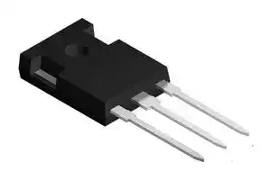
- Transistor Case Style: TO-247
- Operating Temperature Max: 175°C
- Continuous Collector Current: 80A
- Collector Emitter Voltage Max: 1.2kV
- Collector Emitter Saturation Voltage: 1.95V
| Delivery and price | |
|---|---|
| Units per pack | 250 |
| Price | 2.82 € |
| Current stock | 200+ |
| Lead time | 30 days |
**GWA40MS120DF4AG**

Datasheet

Automotive-grade trench gate field-stop, 1200 V, 40 A, low-loss MS series IGBT in a TO-247 long leads package

## **Features**

- AEC-Q101 qualified

**==> picture [90 x 37] intentionally omitted <==**

**----- Start of picture text -----**<br>
~3<br>**----- End of picture text -----**<br>


- 8 μs of short-circuit withstand time at VCC = 800 V, VGE = 15 V,

   - TJ (start) = 175 °C

- VCE(sat) = 1.95 V (typ.) @ IC = 40 A

**==> picture [53 x 6] intentionally omitted <==**

**----- Start of picture text -----**<br>
TO-247 long leads<br>**----- End of picture text -----**<br>


- Tight parameter distribution

- Positive VCE(sat) temperature coefficient

- Low thermal resistance

## **Applications**

- Auxiliary loads

- Thermal management

- PTC heaters

## **Description**

This device is an IGBT developed using an advanced proprietary trench gate fieldstop structure. The device is part of the MS series IGBTs, which represent an evolution of low-loss M series specifically designed for inverter system thanks to the outstanding short-circuit capability at high bus voltage value. Furthermore, the slightly positive VCE(sat) temperature coefficient and very tight parameter distribution result in safer paralleling operation.

## **Product status link**

|**Product summary**|**Product summary**|
|---|---|
|**Order code**|GWA40MS120DF4AG|
|**Marking**|G40MS120DF4AG|
|**Package**|TO-247 long leads|
|**Packing**|Tube|


**DS14215** - **Rev 2** - **February 2023** For further information contact your local STMicroelectronics sales office.

www.st.com

**GWA40MS120DF4AG Electrical ratings**

## **1 Electrical ratings**

**Table 1. Absolute maximum ratings**

|**Symbol**|**Parameter**|**Value**|**Unit**|
|---|---|---|---|
|VCES|Collector-emitter voltage (VGE= 0 V)|1200|V|
|IC|Continuous collector current at TC= 25 °C|80|A|
||Continuous collector current at TC= 100 °C|40||
|ICP(1)|Pulsed collector current|120|A|
|VGE|Gate-emitter voltage|±20|V|
|IF|Continuous forward current at TC= 25 °C|80|A|
||Continuous forward current at TC= 100 °C|40||
|IFP(1)|Pulse forward current|120|A|
|PTOT|Total power dissipation at TC= 25 °C|536|W|
|Tstg|Storage temperature range|-55 to 150|°C|
|TJ|Operating junction temperature range|-55 to 175|°C|


_1. Pulse width is limited by maximum junction temperature._

**Table 2. Thermal data**

|**Symbol**|**Parameter**|**Value**|**Unit**|
|---|---|---|---|
|RthJC|Thermal resistance, junction-to-case, IGBT|0.28|°C/W|
||Thermal resistance, junction-to-case, diode|0.48||
|RthJA|Thermal resistance, junction-to-ambient|50|°C/W|


**DS14215** - **Rev 2**

**page 2/15**

**GWA40MS120DF4AG Electrical characteristics**

## **2 Electrical characteristics**

TC = 25 °C unless otherwise specified.

**Table 3. Static characteristics**

|**Symbol**|**Parameter**|**Test conditions**|**Min.**|**Typ.**|**Max.**|**Unit**|
|---|---|---|---|---|---|---|
|V(BR)CES|Collector-emitter breakdown<br>voltage|VGE= 0 V, IC= 2 mA|1200|||V|
|VCE(sat)|Collector-emitter saturation<br>voltage|VGE= 15 V, IC= 40 A||1.95|2.3|V|
|||VGE= 15 V, IC= 40 A, TJ= 125 °C||2.25|||
|||VGE= 15 V, IC= 40 A, TJ= 175 °C||2.35|||
|VGE(th)|Gate threshold voltage|VCE= VGE, IC= 2 mA|5|6|7|V|
|VF|Forward on-voltage|IF= 40 A||2.4||V|
|||IF= 40 A, TJ= 125 °C||1.85|||
|||IF= 40 A, TJ= 175 °C||1.7|||
|ICES|Collector cut-off current|VGE= 0 V, VCE= 1200 V|||25|µA|
|IGES|Gate-emitter leakage current|VCE= 0 V, VGE= ±20 V|||250|nA|


**Table 4. Dynamic characteristics**

|**Symbol**|**Parameter**|**Test conditions**|**Min.**|**Typ.**|**Max.**|**Unit**|
|---|---|---|---|---|---|---|
|Cies|Input capacitance|VCE= 25 V, f = 1 MHz, VGE= 0 V|-|2700|-|pF|
|Coes|Output capacitance||-|185|-|pF|
|Cres|Reverse transfer capacitance||-|101|-|pF|
|Qg|Total gate charge|VCC= 960 V, IC= 40 A, VGE= 0 to 15 V<br>(seeFigure 28.  Gate charge test circuit)|-|147|-|nC|
|Qge|Gate-emitter charge||-|24|-|nC|
|Qgc|Gate-collector charge||-|79.5|-|nC|


**DS14215** - **Rev 2**

**page 3/15**

**GWA40MS120DF4AG Electrical characteristics**

**Table 5. Switching characteristics (inductive load)**

|**Symbol**|**Parameter**|**Test conditions**|**Min.**|**Typ.**|**Max.**|**Unit**|
|---|---|---|---|---|---|---|
|td(on)|Turn-on delay time|VCC= 600 V, IC= 40 A, VGE= 15 V, RG= 10 Ω<br>(seeFigure 27.  Test circuit for inductive load<br>switching)||35|-|ns|
|tr|Current rise time|||15|-|ns|
|(di/dt)on|Turn-on current slope|||2100|-|A/μs|
|td(off)|Turn-off delay time|||140|-|ns|
|tf|Current fall time|||135|-|ns|
|Eon (1)|Turn-on switching energy|||1.5|-|mJ|
|Eoff (2)|Turn-off switching energy|||3.3|-|mJ|
|Ets|Total switching energy|||4.8|-|mJ|
|td(on)|Turn-on delay time|VCC= 600 V, IC= 40 A, VGE= 15 V, RG= 10 Ω,<br>TJ= 175 °C (seeFigure 27.  Test circuit for inductive<br>load switching)||35|-|ns|
|tr|Current rise time|||18|-|ns|
|(di/dt)on|Turn-on current slope|||1800|-|A/μs|
|td(off)|Turn-off delay time|||150|-|ns|
|tf|Current fall time|||240|-|ns|
|Eon (1)|Turn-on switching energy|||2.8|-|mJ|
|Eoff (2)|Turn-off switching energy|||5.2|-|mJ|
|Ets|Total switching energy|||8.0|-|mJ|
|tsc|Short-circuit withstand<br>time|VCE= 800 V, VGE= 15 V, TJ(start) = 175 °C|8||-|μs|


_1. Including the reverse recovery of the diode._

_2. Including the tail of the collector current._

**Table 6. Diode switching characteristics (inductive load)**

|**Symbol**|**Parameter**|**Test conditions**|**Min.**|**Typ.**|**Max.**|**Unit**|
|---|---|---|---|---|---|---|
|trr|Reverse recovery time|IF= 40 A, VR= 600 V, VGE= 15 V, di/dt = 1000 A/μs<br>(seeFigure 30.  Diode reverse recovery waveform)|-|465|-|ns|
|Qrr|Reverse recovery charge||-|2.8|-|μC|
|Irrm|Reverse recovery current||-|21|-|A|
|dIrr/dt|Peak rate of fall of<br>reverse recovery current<br>during tb||-|1110|-|A/µs|
|Err|Reverse recovery energy||-|1.31|-|mJ|
|trr|Reverse recovery time|IF= 40 A, VR= 600 V, VGE= 15 V, TJ= 175 °C,<br>di/dt = 1000 A/μs (seeFigure 30.  Diode reverse<br>recovery waveform)|-|750|-|ns|
|Qrr|Reverse recovery charge||-|9.45|-|µC|
|Irrm|Reverse recovery current||-|31.2|-|A|
|dIrr/dt|Peak rate of fall of<br>reverse recovery current<br>during tb||-|450|-|A/µs|
|Err|Reverse recovery energy||-|3.9|-|mJ|


**DS14215** - **Rev 2**

**page 4/15**

**GWA40MS120DF4AG Electrical characteristics (curves)**

## **2.1 Electrical characteristics (curves)**

**==> picture [513 x 198] intentionally omitted <==**

**----- Start of picture text -----**<br>
Figure 1. Power dissipation vs case temperature Figure 2. Collector current vs case temperature<br>PTOT GADG160120231021PDT IC GADG160120231021CCT<br> (W)  (A)<br>500<br>VGE ≥ 15 V, TJ ≤ 175 °C  80<br>VGE ≥ 15 V, TJ ≤ 175 °C<br>400<br>60<br>300<br>40<br>200<br>20<br>100<br>0 0<br>25 75 125 175 TC (°C) 25 75 125 175 TC (°C)<br>**----- End of picture text -----**<br>


**==> picture [513 x 199] intentionally omitted <==**

**----- Start of picture text -----**<br>
Figure 3. Output characteristics (TJ = 25 °C) Figure 4. Output characteristics (TJ = 175 °C)<br>IC GADG160120231022OC25 IC GADG160120231022OC175<br> (A)  (A)<br>VGE= 15 V<br>120 120<br>13 V VGE= 15 V<br>13 V<br>80 80<br>11 V<br>11 V<br>40 40<br>9 V 9 V<br>7 V<br>0 7 V 0<br>0 2 4 VCE (V) 0 2 4 VCE (V)<br>**----- End of picture text -----**<br>


## **Figure 5. VCE(sat) vs junction temperature**

**==> picture [195 x 166] intentionally omitted <==**

**----- Start of picture text -----**<br>
VCE(sat) GADG160120231023VCET<br>(V)<br>VGE= 15 V IC = 80 A<br>3.5<br>2.5<br>IC = 40 A<br>1.5<br>IC = 20 A<br>0.5<br>-75 -25 25 75 125 TJ (°C)<br>**----- End of picture text -----**<br>


**Figure 6. VCE(sat) vs collector current**

**==> picture [190 x 166] intentionally omitted <==**

**----- Start of picture text -----**<br>
VCE(sat) GADG160120231023VCEC<br>(V)<br>VGE= 15 V<br>5.5<br>TJ= 175 °C<br>4.5<br>TJ= 25 °C<br>3.5<br>TJ= -55 °C<br>2.5<br>1.5<br>0.5<br>0 40 80 120 IC (A)<br>**----- End of picture text -----**<br>


**DS14215** - **Rev 2**

**page 5/15**

**GWA40MS120DF4AG Electrical characteristics (curves)**

**Figure 7. Collector current vs switching frequency Figure 8. Forward bias safe operating area**

**==> picture [461 x 166] intentionally omitted <==**

**----- Start of picture text -----**<br>
IC GADG180120231038CCS IC GADG160120231023FSOA<br> (A) Rectangular current shape  (A)<br>(duty cycle = 0.5, VCC = 400 V, ICP<br>100 RG = 4.7 Ω, VGE= 0 to 15 V,<br>TJ = 175 °C 10  [2]<br>tp= 1 µs<br>80<br>tp= 10 µs<br>V(BR)CES<br>60 10  [1]<br>VCE(sat) max. tp= 100 µs<br>40 tp= 1 ms<br>TC= 80 °C<br>10  [0]<br>20 TC= 100 °C<br>Single pulse, T C  = 25 °C,<br>TJ ≤ 175 °C, VGE = 15 V<br>0 10  [-1]<br>10 [0] 10 [1] 10 [2] f (kHz) 10  [0] 10  [1] 10  [2] 10  [3] VCE (V)<br>**----- End of picture text -----**<br>


**==> picture [513 x 200] intentionally omitted <==**

**----- Start of picture text -----**<br>
Figure 9. Transfer characteristics Figure 10. Diode VF vs forward current<br>IC GADG160120231024TCH VF GADG160120231024DVF<br> (A)  (V) TJ= -40°C<br>VCE= 5 V<br>80<br>TJ= 25 °C<br>4<br>60<br>TJ= 25 °C TJ= 175 °C<br>40<br>2<br>TJ= 175 °C<br>20<br>0 0<br>1 4 7 10 13 VGE (V) 0 40 80 IF (A)<br>**----- End of picture text -----**<br>


**==> picture [513 x 199] intentionally omitted <==**

**----- Start of picture text -----**<br>
Figure 11. Normalized VGE(th) vs junction temperature Figure 12. Normalized V(BR)CES vs junction temperature<br>VGE(th) GADG160120231025NVGE V(BR)CES GADG160120231025NVBR<br> (Norm.)  (Norm.)<br>VGE = VCE IC = 1 mA<br>1.1<br>IC = 2 mA<br>1.0<br>1.0<br>0.8<br>0.9<br>0.6 0.8<br>-75 -25 25 75 125 TJ (°C) -75 -25 25 75 125 TJ (°C)<br>**----- End of picture text -----**<br>


**DS14215** - **Rev 2**

**page 6/15**

**GWA40MS120DF4AG Electrical characteristics (curves)**

**==> picture [513 x 198] intentionally omitted <==**

**----- Start of picture text -----**<br>
Figure 13. Capacitance variations Figure 14. Gate charge vs gate-emitter voltage<br>C  GADG160120231026CVR VGE GADG160120231026GCGE<br>(pF)  (V) VCC = 960 V, IC = 40 A,<br>IG = 18 mA<br>10  [4] 16<br>Cies<br>10  [3] 12<br>10  [2] 8<br>Coes<br>Cres<br>10  [1] f = 1 MHz 4<br>10  [0] 0<br>10 [-1] 10 [0] 10 [1] 10 [2] VCE (V) 0 50 100 150 Qg (nC)<br>**----- End of picture text -----**<br>


**==> picture [513 x 415] intentionally omitted <==**

**----- Start of picture text -----**<br>
Figure 15. Switching energy vs collector current Figure 16. Switching energy vs gate resistance<br>E  GADG160120231027SLC E  GADG160120231031SLG<br>(mJ) VCC = 600 V, RG = 10 Ω,  (mJ) VCC = 600 V, VGE = 15 V, IC = 40 A,<br>VGE = 15 V, TJ=175  ℃ Eon TJ = 175  ℃<br>7<br>Eoff<br>8 6<br>Eoff<br>5<br>Eon<br>4 4<br>3<br>0 2<br>0 30 60 IC (A) 0 10 20 30 40 RG (Ω)<br>Figure 17. Switching energy vs temperature Figure 18. Switching energy vs collector emitter voltage<br>E  GADG160120231029SLT E  GADG160120231031SLV<br>(mJ) VCC = 600 V, IC = 40 A, RG = 10 Ω,  (mJ) IC = 40 A, TJ=175  ℃<br>VGE = 15 V  RG= 10 Ω, VGE = 15 V<br>5<br>Eoff Eoff<br>4.5 4<br>3<br>Eon Eon<br>2.5 2<br>1<br>0.5 0<br>0 50 100 150 TJ (°C) 500 600 700 800 900 VCE (V)<br>**----- End of picture text -----**<br>


**DS14215** - **Rev 2**

**page 7/15**

**GWA40MS120DF4AG Electrical characteristics (curves)**

**==> picture [513 x 198] intentionally omitted <==**

**----- Start of picture text -----**<br>
Figure 19. Switching times vs collector current Figure 20. Switching times vs gate resistance<br>t  GADG160120231032STC t  GADG160120231033STR<br>(ns) VCC = 600 V, VGE = 15 V, RG = 10 Ω,  (ns) VCC = 600 V, VGE = 15 V, IC = 40 A,<br>TJ = 175  ℃ TJ = 175  ℃<br>600<br>500 td(off)<br>tf<br>tf<br>400<br>300<br>td(off) 200<br>100 0<br>0 25 50 75 IC (A) 0 10 20 30 40 RG (Ω)<br>**----- End of picture text -----**<br>


**Figure 21. Reverse recovery current vs diode current slope**

**==> picture [200 x 166] intentionally omitted <==**

**----- Start of picture text -----**<br>
Irrm GADG160120231033RRC<br> (A) 6 4<br>35<br>25<br>15<br>0 800 1600 2400 di/dt (A/µs)<br>**----- End of picture text -----**<br>


**Figure 22. Reverse recovery time vs diode current slope**

**==> picture [205 x 165] intentionally omitted <==**

**----- Start of picture text -----**<br>
trr GADG160120231034RRT<br> (ns) 6<br>1100<br>1000<br>900<br>800<br>700<br>600<br>0 800 1600 2400 di/dt (A/µs)<br>**----- End of picture text -----**<br>


**Figure 23. Reverse recovery charge vs diode current slope**

**==> picture [205 x 165] intentionally omitted <==**

**----- Start of picture text -----**<br>
Qrr GADG160120231035RRQ<br> (µC) 6<br>4<br>9.6<br>9.2<br>8.8<br>8.4<br>0 800 1600 2400 di/dt (A/µs)<br>**----- End of picture text -----**<br>


**Figure 24. Reverse recovery energy vs diode current slope**

**==> picture [205 x 165] intentionally omitted <==**

**----- Start of picture text -----**<br>
Err GADG160120231037RRE<br> (mJ) 6<br>4<br>4<br>3<br>2<br>0 800 1600 2400 di/dt (A/µs)<br>**----- End of picture text -----**<br>


**DS14215** - **Rev 2**

**page 8/15**

**GWA40MS120DF4AG Electrical characteristics (curves)**

**==> picture [440 x 197] intentionally omitted <==**

**----- Start of picture text -----**<br>
Figure 25. Maximum transient thermal impedance Figure 26. Maximum transient thermal impedance<br>for IGBT for diode<br>(°C/W)ZthJC el a a GADG180120231008ZTH_IGBT a|| (°C/W)ZthJC FEaTt GADG180120231009ZTH_diode<br>PO |<br>PTa TTT T PPTPiPPP P duty=0.5 OeeTer TTT<br>Co duty=0.5 eT etsee e e oer<br>10  [-1] eee 10  [-1] cee Ml ll<br>Sree mnimuamaetieoe SUNN 4<br>fo ie NSE 4 FER ENE, 3 HoH<br>Fog Het nr AAA NN 3 a | ana 0.05 0  .  1 TANioc AmatN COO|Ty<br>2<br>ee 0.05 fon NS 2 imma ae nil) all iam<br>10  [-2] CCC i 10  [-2] N20<br>aN RthJC = 0.28  ℃/W 00 NAT RthJC = 0.48  ℃/W<br>nnyTTI ai imate duty = t on / T cali citeatiiaet| duty = t on / T<br>Single pulse<br>FA TTT a=<br>Single pulse | ton | TTI | ton<br>T T<br>10  [-3] 10  [-3]<br>10  [-6] 10  [-5] 10  [-4] 10  [-3] 10  [-2] 10  [-1] tp (s) 10  [-6] 10  [-5] 10  [-4] 10  [-3] 10  [-2] 10  [-1] tp (s)<br>**----- End of picture text -----**<br>


**DS14215** - **Rev 2**

**page 9/15**

**GWA40MS120DF4AG Test circuits**

## **3 Test circuits**

**Figure 27.  Test circuit for inductive load switching**

**==> picture [194 x 149] intentionally omitted <==**

**----- Start of picture text -----**<br>
A A<br>C<br>L=100 μH<br>G<br>E B<br>B<br>C 3.3μF 1000μF VCC<br>G D.U.T<br>RG<br>K E<br>GND1 GND2<br>(signal ground) (power ground) HB650_4_leads<br>**----- End of picture text -----**<br>


**Figure 28.  Gate charge test circuit**

**==> picture [58 x 82] intentionally omitted <==**

**==> picture [98 x 84] intentionally omitted <==**

**==> picture [59 x 5] intentionally omitted <==**

**----- Start of picture text -----**<br>
GADG030820201115SA<br>**----- End of picture text -----**<br>


**==> picture [513 x 198] intentionally omitted <==**

**----- Start of picture text -----**<br>
Figure 29.  Switching waveform Figure 30.  Diode reverse recovery waveform<br>90%<br>VG 10%<br>90%<br>VCE tr(Voff) 10%<br>tcross 10<br>90%<br>IC td(on)ton tr(Ion) td(off)toff tf 10%<br>AM01506v1 GADG140820170937SA<br>**----- End of picture text -----**<br>


**DS14215** - **Rev 2**

**page 10/15**

**GWA40MS120DF4AG Package information**

## **4 Package information**

In order to meet environmental requirements, ST offers these devices in different grades of ECOPACK packages, depending on their level of environmental compliance. ECOPACK specifications, grade definitions and product status are available at: www.st.com. ECOPACK is an ST trademark.

## **4.1 TO-247 long leads package information**

**Figure 31. TO-247 long leads package outline**

**==> picture [130 x 68] intentionally omitted <==**

**==> picture [72 x 87] intentionally omitted <==**

8463846_3

**DS14215** - **Rev 2**

**page 11/15**

**GWA40MS120DF4AG TO-247 long leads package information**

**Table 7. TO-247 long leads package mechanical data**

|**Di**|**mm**|**mm**|**mm**|
|---|---|---|---|
|**m.**|**Min.**|**Typ.**|**Max.**|
|A|4.90|5.00|5.10|
|A1|2.31|2.41|2.51|
|A2|1.90|2.00|2.10|
|b|1.16||1.26|
|b2|||3.25|
|b3|||2.25|
|c|0.59||0.66|
|D|20.90|21.00|21.10|
|E|15.70|15.80|15.90|
|E2|4.90|5.00|5.10|
|E3|2.40|2.50|2.60|
|e|5.34|5.44|5.54|
|L|19.80|19.92|20.10|
|L1|||4.30|
|P|3.50|3.60|3.70|
|Q|5.60||6.00|
|S|6.05|6.15|6.25|
|aaa||0.04|0.10|


**DS14215** - **Rev 2**

**page 12/15**

**GWA40MS120DF4AG**

## **Revision history**

**Table 8. Document revision history**

|**Date**|**Revision**|**Changes**|
|---|---|---|
|24-Jan-2023|1|First release.|
|01-Feb-2023|2|ModifiedTable 5. Switching characteristics (inductive load)andTable 6. Diode<br>switching characteristics (inductive load).|


**DS14215** - **Rev 2**

**page 13/15**

**GWA40MS120DF4AG Contents**

## **Contents**

|**1**|**Electrical ratings . . . . . . . . . . . . . . . . . . . . . . . . . . . . . . . . . . . . . . . . . . . . . . . . . . . . . . . . . . . . . . . . . .2**|
|---|---|
|**2**|**Electrical characteristics. . . . . . . . . . . . . . . . . . . . . . . . . . . . . . . . . . . . . . . . . . . . . . . . . . . . . . . . . . .3**|
||**2.1**<br>Electrical characteristics (curves) . . . . . . . . . . . . . . . . . . . . . . . . . . . . . . . . . . . . . . . . . . . . . . . . . 5|
|**3**|**Test circuits . . . . . . . . . . . . . . . . . . . . . . . . . . . . . . . . . . . . . . . . . . . . . . . . . . . . . . . . . . . . . . . . . . . . . .10**|
|**4**|**Package information. . . . . . . . . . . . . . . . . . . . . . . . . . . . . . . . . . . . . . . . . . . . . . . . . . . . . . . . . . . . . .11**|
||**4.1**<br>TO-247 long leads package information. . . . . . . . . . . . . . . . . . . . . . . . . . . . . . . . . . . . . . . . . . . 11|
|**Revision history . . . . . . . . . . . . . . . . . . . . . . . . . . . . . . . . . . . . . . . . . . . . . . . . . . . . . . . . . . . . . . . . . . . . . . .13**||


**DS14215** - **Rev 2**

**page 14/15**

**GWA40MS120DF4AG**

## **IMPORTANT NOTICE – READ CAREFULLY**

STMicroelectronics NV and its subsidiaries (“ST”) reserve the right to make changes, corrections, enhancements, modifications, and improvements to ST products and/or to this document at any time without notice. Purchasers should obtain the latest relevant information on ST products before placing orders. ST products are sold pursuant to ST’s terms and conditions of sale in place at the time of order acknowledgment.

Purchasers are solely responsible for the choice, selection, and use of ST products and ST assumes no liability for application assistance or the design of purchasers’ products.

No license, express or implied, to any intellectual property right is granted by ST herein.

Resale of ST products with provisions different from the information set forth herein shall void any warranty granted by ST for such product.

ST and the ST logo are trademarks of ST. For additional information about ST trademarks, refer to www.st.com/trademarks. All other product or service names are the property of their respective owners.

Information in this document supersedes and replaces information previously supplied in any prior versions of this document.

© 2023 STMicroelectronics – All rights reserved

**DS14215** - **Rev 2**

**page 15/15**
Updated at April 21, 2026
STMicroelectronics is a global leader in the semiconductor industry, recognized for developing highly integrated, energy-efficient solutions that power modern electronics. With a strong focus on innovation, ST provides a comprehensive portfolio of microelectronics that address the demanding requirements of industrial, automotive, communications, and consumer applications. Our extensive selection of STMicroelectronics components is built around a robust lineup of discrete semiconductors and circuit protection devices. We offer a wide variety of single MOSFETs, Schottky diodes, and fast and ultrafast recovery rectifier diodes, designed to deliver exceptional efficiency and thermal performance in power management and conversion systems. For robust circuit protection, our inventory features hundreds of transient voltage suppressors and TVS diodes that safeguard sensitive electronic components against destructive voltage spikes. In addition to core power discretes like TRIACs, SCRs, bipolar transistors, and single IGBTs, our STMicroelectronics range includes specialized integrated passive filters and MEMS sensors. Furthermore, ST offers advanced integrated passive devices, such as baluns and RF filters, which utilize high-quality monolithic RF IPD processes on glass or high-resistance silicon substrates. These components provide competitive cost structures, reduced power losses, and simplified RFIC-to-antenna matching, ensuring optimal system performance and delivering the reliability required for next-generation wireless and power designs.
About Novapart
Novapart is a B2B electronic component broker specialising in stock shortages and cost reduction. We source hard-to-find parts and identify compliant alternatives across a catalogue of 410,000+ components from 500+ manufacturers.
Learn more →Stock Shortage Specialist
When a component is unavailable, discontinued or has an unacceptable lead time, we tap into our network of vetted European and Asian distributors to source what you need — without compromising on quality or traceability.
Request a quote →Compliant Alternatives
We identify pin-to-pin, electrically equivalent substitutes that meet the same certifications (RoHS, AEC-Q100, REACH) as your original specification — validated against datasheets, not just part numbers. Often at a lower cost.
BOM Analysis service →