
Image not available
Illustrative purposes only

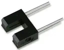
GP1S53VJ000F
Transmissive Photo Interrupter, Phototransistor, Through Hole, 5 mm, 0.5 mm, 50 mA, 6 V
⚠️ Reference pricing provided. In case of supply shortages, we will connect you with our trusted procurement partners to ensure your project's continuity.
- Manufacturer: SHARP
- Product type: Transmissive Photo Interrupters
- Gap Width: 5mm
- Product Range: GP1S53VJ000F
- Sensor Output: Phototransistor
- Aperture Width: 0.5mm
- Forward Voltage: 1.2V
- Sensor Mounting: Through Hole
- Forward Current If: 50mA
- Reverse Voltage Vr: 6V
| Delivery and price | |
|---|---|
| Units per pack | 2500 |
| Price | 0.349 € |
| Current stock | 10+ |
| Lead time | 30 days |
Datasheet

**GP1S53V/GP1S58V**

## **GP1S53V/GP1S58V**

## **Compact Photointerrupter**

## I **Features**

1. Compact type

2. High sensing accuracy (Slit width : 0.5mm )

3. PWB direct mounting type

4. With positioning pin ( **GP1S58V** )

## I **Outline Dimensions**

## I **Applications**

1. OA equipment, such as FDDs, printers, facsimiles

2. VCRs

3. Optoelectronic switches

(Unit : mm )

**==> picture [433 x 238] intentionally omitted <==**

**----- Start of picture text -----**<br>
GP1S53V GP1S58V<br>Internal connection 13.7 [+] - [ 0.3] 0.3 Internal connection 13.7 [+] - [ 0.3] 0.3<br>diagram 5.0 [+] - [0.2] 0.1 diagram 5.0 [+] - [0.2] 0.1<br>3 2 3 2<br>4 1 4 1<br>1  Anode 3  Collector 1  Anode 3  Collector<br>2  Cathode 4  Emitter 2  Cathode 4  Emitter<br>A-A ’ section B-B  ’ section A-A ’ section B-B ’ section<br>0.5 A B 0.5 0.5 A B 0.5<br>0.45 [+] - [ 0.3] 0.1 A ’ [B] [’] 0.4 [+] - [ 0.3] 0.1 0.45 [+] - [ 0.3] 0.1 A ’ [B] [’] 0.4 [+] - [ 0.3] 0.1<br>(2.54) (10.3) (2.54) (10.3)<br>4 6.5<br>* Unspecified tolerances  * Unspecified tolerances<br> shall be as follows  ; 4 1  shall be as follows ; 1<br>Dimensions(d) Tolerance Dimensions(d) Tolerance<br>d <=  6.0 ±  0.1 d <=  6.0 ±  0.1 2<br>6.0  <  d <= 18.0 ±  0.2 6.0  <  d <= 18.0 ±  0.2 2 - φ 0.7<br>*  ( ) : Reference dimensions 3 2 *  ( )  : Reference dimensions 3 2.5<br>C1 C1<br>5.2 5.2<br>3.5 (2.5) 1.5 3.5 (2.5) 1.5<br>10 7.5 (Sensor center) 10 7.5 (Sensor center)<br>MIN 10 MIN 10 2-0.7<br>2.0<br>S53 S58<br>**----- End of picture text -----**<br>


## I **Absolute Maximum Ratings**

## (Ta= 25˚C)

||Parameter|Symbol|Rating<br>|Unit|
|---|---|---|---|---|
|Input<br> <br>*1 <br> <br>|Forward current|IF|50<br>|mA|
||Peak forward current|IFM|1|A|
||Reverse voltage|VR|6|V|
||Power dissipation|P|75<br>|mW|
|Output<br> <br> <br> <br>|Collector-emitter voltage|VCEO|35|V|
||Emitter-collector voltage|VECO|6|V|
||Collector current|IC|20<br>|mA|
||Collector power dissipation|PC|75<br>|mW|
||Operating temperature|Topr|- 25 to + 85|˚C|
||Storage temperature|Tstg|- 40 to + 100|˚C|
|*2|Solderingtemperature|Tsol|260|˚C|


- *1 Pulse width<=100 µ s, Duty ratio= 0.01

- *2 For 5 seconds

- “ In the absence of confirmation by device specification sheets, SHARP takes no responsibility for any defects that occur in equipment using any of SHARP's devices, shown in catalogs, data books, etc. Contact SHARP in order to obtain the latest version of the device specification sheets before using any SHARP's device. ”

**GP1S53V/GP1S58V**

## I **Electro-optical Characteristics**

(Ta = 25˚C)

||||||||||
|---|---|---|---|---|---|---|---|---|
|**GP1S53V/GP1S58V**|||||||||
|(Ta = 25˚C)<br>I**Electro-optical Characteristics**|||||||||
||Parameter||Symbol|Conditions|MIN.|TYP.|MAX.|Unit|
|Input|Forward voltage||VF|IF= 20mA|-|1.25|1.4|V|
||Peak forward voltage||V FM|IFM= 0.5A|-|3|4|V|
||Reverse current||IR|VR= 3V|-|-|10|µA|
|Output|Collector dark current||ICEO|VCE= 20V|-|1|100|nA|
|Transfer<br>charac-<br>teristics|Collector Current||Ic|IF= 20mA, VCE= 5V|0.5|-|1.5|mA|
||Collector-emitter saturation voltage||VCE(sat)|IF= 40mA, IC= 0.2mA|-|-|0.4|V|
||Response time|Rise time|tr|RL= 100Ω<br>VCE= 2V, I C= 2mA|-|3|15|µs|
|||Fall time|tf||-|4|20|µs|


**==> picture [169 x 174] intentionally omitted <==**

**----- Start of picture text -----**<br>
Fig. 1 Forward Current vs. Ambient<br>       Temperature<br>60<br>50<br>40<br>30<br>20<br>10<br>0<br>- 25 0 25 50 75 85 100<br>Ambient temperature T a (˚C)<br> (mA)<br> F<br>Forward current I<br>**----- End of picture text -----**<br>


## **Fig. 3 Peak Forward Current vs. Duty Ratio**

**==> picture [167 x 154] intentionally omitted <==**

**----- Start of picture text -----**<br>
Pulse width <= 100 µ  s<br>2000 T a= 25˚C<br>1000<br>500<br>200<br>100<br>50<br>20<br>5 10 [- 2] 2 5 10 [- 1] 2 5 10 [0]<br>Duty ratio<br> (mA)<br>FM<br>Peak forward current I<br>**----- End of picture text -----**<br>


**==> picture [153 x 19] intentionally omitted <==**

**----- Start of picture text -----**<br>
Fig. 2 Collector Power Dissipation vs.<br>       Ambient Temperature<br>**----- End of picture text -----**<br>


**==> picture [165 x 339] intentionally omitted <==**

**----- Start of picture text -----**<br>
120<br>100<br>80<br>75<br>60<br>40<br>20<br>0<br>- 25 0 25 50 75 85 100<br>Ambient temperature Ta (˚C)<br>Fig. 4 Forward Current vs.<br>       Forward Voltage<br>500<br>200 T a= 75˚C 25˚C0˚C<br>50˚C - 25˚C<br>100<br>50<br>20<br>10<br>5<br>2<br>1<br>0 0.5 1 1.5 2 2.5 3 3.5<br>Forward voltage V F (V)<br> ( mW )<br> C<br>Collector power dissipation P<br> (mA)<br> F<br>Forward current I<br>**----- End of picture text -----**<br>


**Fig. 4 Forward Current vs. Forward Voltage**

**GP1S53V/GP1S58V**

## **Fig. 5 Collector Current vs. Forward Current**

## **Fig.6  Collector Current vs.**

**==> picture [160 x 166] intentionally omitted <==**

**----- Start of picture text -----**<br>
       Collector-emitter Voltage<br>5<br>T a= 25˚C  IF = 50mA<br>4<br>40mA<br>3 30mA<br>2 20mA<br>1 10mA<br>0<br>0 1 2 3 4 5 6 7 8 9 10<br>Collector-emitter voltage VCE (V)<br> (mA)<br>C<br>Collector current I<br>**----- End of picture text -----**<br>


**==> picture [158 x 156] intentionally omitted <==**

**----- Start of picture text -----**<br>
5<br>V CE= 5V<br>T a= 25˚C<br>4<br>3<br>2<br>1<br>0<br>0 10 20 30 40 50<br>Forward current I F (mA)<br> (mA)<br>C<br>Collector current I<br>**----- End of picture text -----**<br>


## **Fig. 7 Collector Current vs. Ambient Temperature**

**Fig. 8 Collector-emitter Saturation Voltage vs. Ambient Temperature**

**==> picture [411 x 340] intentionally omitted <==**

**----- Start of picture text -----**<br>
3.0 0.3<br>IF = 20mA IF = 40mA<br>V CE= 5V IC= 0.2mA<br>2.5 0.25<br>2.0 0.2<br>1.5 0.15<br>1.0 0.1<br>0.5 0.05<br>0 0<br>- 25 0 25 50 75 100 - 25 0 25 50 75 100<br>Ambient temperature T a (˚C) Ambient temperature T a (˚C)<br>Fig. 9 Response Time vs.<br>       Load Resistance Test Circuit for Response Time<br>100<br>V CE= 2V<br>50 IC= 2mA<br>T a= 25˚C<br>20<br>10 VCC Input<br>5 t f Input RD RL<br>Output Output 10 %<br>2 t d t r 90 %<br>1 td ts<br>tr tf<br>0.5<br>t s<br>0.2<br>0.1<br>0.01 0.02 0.05 0.1 0.2 0.5 1 2 5 10<br>Load resistance RL [ (k] [ Ω] [)]<br> (V)<br> (mA)<br> C  CE(sat)<br>Collector current I V<br>Collector-emitter saturation voltage<br> s)<br> µ<br>Response time (<br>**----- End of picture text -----**<br>


## **Fig. 9 Response Time vs.**

**GP1S53V/GP1S58V**

## **Fig.10 Frequency Response**

**==> picture [166 x 341] intentionally omitted <==**

**----- Start of picture text -----**<br>
V CE= 2V<br>IC= 2mA<br>0 T a= 25˚C<br>- 5<br>R L= 10k Ω 1k Ω 100 Ω<br>- 10<br>- 15<br>- 20<br>2 5 10 [3] 2 5 10 [4] 2 5 10 [5] 2 5 10 [6]<br>Frequency f (Hz )<br>Fig.12 Relative Collector Current vs.<br>       Shield Distance (1)<br>IF = 20mA, VCE= 5V<br>T a= 25˚C L<br>100<br>Detector<br>Shield<br>- +<br>0<br>50 (Detector center )<br>0<br>- 2.5 - 2.0 - 1.5 - 1 - 0.5 0 0.5 1 1.5 2 2.5<br>Shield distance L ( mm )<br>Voltage gain Av ( dB )<br>Relative collector current ( % )<br>**----- End of picture text -----**<br>


## **Fig.12 Relative Collector Current vs. Shield Distance (1)**

**==> picture [133 x 19] intentionally omitted <==**

**----- Start of picture text -----**<br>
Fig.11 Collector Dark Current vs.<br>       Ambient Temperature<br>**----- End of picture text -----**<br>


**==> picture [168 x 342] intentionally omitted <==**

**----- Start of picture text -----**<br>
10 [-] [6]<br>5 V CE= 20V<br>2<br>10 [-] [7]<br>5<br>2<br>10 [-] [8]<br>5<br>2<br>10 [-] [9]<br>5<br>2<br>10 [-] [10]<br>- 25 0 25 50 75 100<br>Ambient temperature T a (˚C)<br>Fig.13 Relative Collector Current vs.<br>       Shield Distance (2)<br>IF = 20mA, V CE= 5V<br>T a= 25˚C<br>100 Shield<br>-<br>0<br>+<br>Detector<br>50<br>0<br>- 2 - 1 0 1 2<br>Shield distance L ( mm )<br> (A)<br>CEO<br>Collector dark current I<br>L<br>(Detector center )<br>Relative collector current ( % )<br>**----- End of picture text -----**<br>


## **Fig.13 Relative Collector Current vs. Shield Distance (2)**

## I **Precautions for Use**

- (1) In case of cleaning, use only the following type of cleaning solvent. Ethyl alcohol, methyl alcohol, Isopropyl alcohol

- (2) As for other general cautions, refer to the chapter “ Precautions for Use”.

**Application Circuits**

## **NOTICE**

- G The circuit application examples in this publication are provided to explain representative applications of SHARP devices and are not intended to guarantee any circuit design or license any intellectual property rights.  SHARP takes no responsibility for any problems related to any intellectual property right of a third party resulting from the use of SHARP's devices.

- G Contact SHARP in order to obtain the latest device specification sheets before using any SHARP device. SHARP reserves the right to make changes in the specifications, characteristics, data, materials, structure, and other contents described herein at any time without notice in order to improve design or reliability.  Manufacturing locations are also subject to change without notice.

- G Observe the following points when using any devices in this publication. SHARP takes no responsibility for damage caused by improper use of the devices which does not meet the conditions and absolute maximum ratings to be used specified in the relevant specification sheet nor meet the following conditions:

- (i) The devices in this publication are designed for use in general electronic equipment designs such as: --- Personal computers

- --- Office automation equipment

- --- Telecommunication equipment [terminal]

- --- Test and measurement equipment

- --- Industrial control

- --- Audio visual equipment

- --- Consumer electronics

- (ii)Measures such as fail-safe function and redundant design should be taken to ensure reliability and safety when SHARP devices are used for or in connection with equipment that requires higher reliability such as:

- --- Transportation control and safety equipment (i.e., aircraft, trains, automobiles, etc.)

- --- Traffic signals

- --- Gas leakage sensor breakers

- --- Alarm equipment

- --- Various safety devices, etc.

- (iii)SHARP devices shall not be used for or in connection with equipment that requires an extremely high level of reliability and safety such as:

- --- Space applications

- --- Telecommunication equipment [trunk lines]

- --- Nuclear power control equipment

- --- Medical and other life support equipment (e.g., scuba).

- G Contact a SHARP representative in advance when intending to use SHARP devices for any "specific" applications other than those recommended by SHARP or when it is unclear which category mentioned above controls the intended use.

- G If the SHARP devices listed in this publication fall within the scope of strategic products described in the Foreign Exchange and Foreign Trade Control Law of Japan, it is necessary to obtain approval to export such SHARP devices.

- G This publication is the proprietary product of SHARP and is copyrighted, with all rights reserved. Under the copyright laws, no part of this publication may be reproduced or transmitted in any form or by any means, electronic or mechanical, for any purpose, in whole or in part, without the express written permission of SHARP.  Express  written permission is also required before any use of this publication may be made by a third party.

- G Contact and consult with a SHARP representative if there are any questions about the contents of this publication.

115
Updated at February 9, 2023
About Novapart
Novapart is a B2B electronic component broker specialising in stock shortages and cost reduction. We source hard-to-find parts and identify compliant alternatives across a catalogue of 410,000+ components from 500+ manufacturers.
Learn more →Stock Shortage Specialist
When a component is unavailable, discontinued or has an unacceptable lead time, we tap into our network of vetted European and Asian distributors to source what you need — without compromising on quality or traceability.
Request a quote →Compliant Alternatives
We identify pin-to-pin, electrically equivalent substitutes that meet the same certifications (RoHS, AEC-Q100, REACH) as your original specification — validated against datasheets, not just part numbers. Often at a lower cost.
BOM Analysis service →