
Image not available
Illustrative purposes only

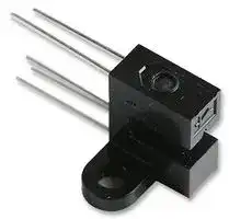
GP1A51HRJ00F
Transmissive Photo Interrupter, Photo / Optical IC, Through Hole, 3 mm, 0.5 mm, 50 mA, 6 V
⚠️ Reference pricing provided. In case of supply shortages, we will connect you with our trusted procurement partners to ensure your project's continuity.
- Manufacturer: SHARP
- Product type: Transmissive Photo Interrupters
- Gap Width: 3mm
- Product Range: GP1A51HRJ00F
- Sensor Output: Photo / Optical IC
- Aperture Width: 0.5mm
- Forward Voltage: 1.1V
- Sensor Mounting: Through Hole
- Forward Current If: 50mA
- Reverse Voltage Vr: 6V
| Delivery and price | |
|---|---|
| Units per pack | 100 |
| Price | 0.966 € |
| Current stock | 10+ |
| Lead time | 30 days |
Datasheet

**GP1A51HRJ00F**

## **GP1A51HRJ00F**

## ■ **Description**

**GP1A51HRJ00F** is a standard, OPIC output, transmissive photointerrupter with opposing emitter and detector in a case, providing non-contact sensing.  For this family of devices, the emitter and detector are inserted in a case, resulting in a through-hole design.

The case includes additional screw fixing holes, on both sides 3.2mm diameter.

## **Gap : 3mm, Slit : 0.5mm *OPIC Output Case package Transmissive Photointerrupter**

## ■ **Agency approvals/Compliance**

1. Compliant with RoHS directive

## ■ **Applications**

1. General purpose detection of object presence or motion.

2. Example : Printer, FAX, Optical storage unit

## ■ **Features**

1. Transmissive with OPIC output

2. Highlights:

- Verical Slit for alternate motion detection

- Output Low Level at intercepting optical path

- Includes additional screw fi xing holes

3. Key Parameters:

- Gap Width : 3mm

- Slit Width (detector side) : 0.5mm

- Package : 12.2×10×18mm

4. RoHS directive compliant

* "OPIC"(Optical IC) is a trademark of the SHARP Corporation. An OPIC consists of a light-detecting element and a signalprocessing Notice The content of data sheet is subject to change without prior notice. In the absence of confi rmation by device specifi cation sheets, SHARP takes no responsibility for any defects that may occur in equipment using any SHARP ~~pT~~ devices shown in catalogs, data books, etc. Contact SHARP in order to obtain the latest device specifi cation sheets before using any SHARP device. Sheet No.: D3-A03601 F EN 1 Date Oct. 3. 2005 © SHARP Corporation

**GP1A51HRJ00F**

## ■ **Internal Connection Diagram**

**==> picture [213 x 119] intentionally omitted <==**

**----- Start of picture text -----**<br>
Top view<br>Voltage regulator<br>3 2<br>(15kΩ) 1 Anode<br>2 Cathode<br>4 3 VCC<br>4 VO<br>5 GND<br>Amp<br>5 1<br>**----- End of picture text -----**<br>


## ■ **Outline Dimensions**

(Unit : mm)

**==> picture [300 x 318] intentionally omitted <==**

**----- Start of picture text -----**<br>
Top view<br>12.2 [±][0.3]<br>2<br>3− [+][0.2] 0.1<br>A-Aʼ section B-Bʼ section<br>5<br>0.5 0.5<br>2−φ3.2 [±][0.2] A B Model No.<br>Date<br>5−0.45− [+][0.3] 0.1 Aʼ Bʼ code<br>(1.5)<br>2−(1.27) (9.2)<br>12<br>18 5 1<br>4<br>3 2<br>• Unspecified tolerance shall be as<br>follows ;<br>Dimensions (d) Tolerance<br>d≤6 ±0.1<br>6<d≤18 ±0.2<br>• ( ) : Reference dimensions<br>3.5 2.5 1.5<br>(Detctor center)<br>7 6 10 7.5<br>1A51HR<br>MIN.<br>9<br>**----- End of picture text -----**<br>


Product mass : approx. 0.65g

Dip soldering material : Sn−3Ag−0.5Cu

Sheet No.: D3-A03601 F EN

2

**GP1A51HRJ00F**

## Date code (2 digit)

|1st digit|1st digit|2nd digit|2nd digit|
|---|---|---|---|
|Year of  production||Month of production||
|A.D.|Mark|Month|Mark|
|2000|0|1|1|
|2001|1|2|2|
|2002|2|3|3|
|2003|3|4|4|
|2004|4|5|5|
|2005|5|6|6|
|2006|6|7|7|
|2007|7|8|8|
|2008|8|9|9|
|2009|9|10|X|
|2010|0|11|Y|
|:|:|12|Z|


repeats in a 10 year cycle

## Country of origin

Japan, Indonesia or Philippines (Indicated on the packing case)

Sheet No.: D3-A03601 F EN

3

**GP1A51HRJ00F**

|■**Absolute Maximum Ratings**<br>(Ta=25˚C)|■**Absolute Maximum Ratings**<br>(Ta=25˚C)|■**Absolute Maximum Ratings**<br>(Ta=25˚C)|■**Absolute Maximum Ratings**<br>(Ta=25˚C)|■**Absolute Maximum Ratings**<br>(Ta=25˚C)|
|---|---|---|---|---|
||Parameter|Symbol|Rating|Unit|
|Input|∗1Forward current|IF|50|mA|
||∗1, 2Peak forward current|IFM|1|A|
||Reverse voltage|VR|6|V|
||Power dissipation|P|75|mW|
|Output|Supply voltage|VCC|−0.5 to+17|V|
||Output current|IO|50|mA|
||Power dissipation|PO|250|mW|
|Operating temperature||Topr|−25 to+85|˚C|
|Storage temperature||Tstg|−40 to+100|˚C|
|∗3Soldering temperature||Tsol|260|˚C|


∗1 The derating factors of absolute maximum ratings due to ambient temperature are shown in Fig. 1, 2, 3

∗2 Pulse width ≤ 100μs, Duty ratio=0.01

∗3 For 5s or less

## ■ **Electro-optical Characteristics**

|■**Ele**|**tr**|**o-optical Characteristics**|**o-optical Characteristics**|**o-optical Characteristics**|(Ta=25˚C)|(Ta=25˚C)|(Ta=25˚C)|(Ta=25˚C)|
|---|---|---|---|---|---|---|---|---|
|||Parameter|Symbol|Condition|MIN.|TYP.|MAX.|Unit|
|Input||Forward voltage|VF|IF=5mA|−|1.1|1.4|V|
|||Reverse current|IR|VR=3V|−|−|10|μA|
|Output||Operating supply voltage|VCC|−|4.5|−|17|V|
|||Low level output voltage|VOL|VCC=5V, IOL=16mA, IF=0|−|0.15|0.4|V|
|||High level output voltage|VOH|VCC=5V, IF=5mA|4.9|−|−|V|
|||Low level supply current|ICCL|VCC=5V, IF=0|−|1.7|3.8|mA|
|||High level supply current|ICCH|VCC=5V, IF=5mA|−|0.7|2.2|mA|
|Transfer<br>charac-<br>teristics|∗4|"Low→High" threshold input current|IFLH|VCC=5V|−|1|5|mA|
||∗5|Hysteresis|IFHL/IFLH|VCC=5V|0.55|0.75|0.95|−|
||Responce time<br>6<br>∗|"Low→High" Propagation delay time|tPLH|VCC=5V, IF=5mA, RL=280Ω|−|3|9|μs|
|||"High→Low" Propagation delay time|tPHL||−|5|15||
|||Rise time|tr||−|0.1|0.5||
|||Fall time|tf||−|0.05|0.5||


∗4 IFLH represents forward current when output goes from "Low" to "High".

∗5 IFHL represents forward current when output goes from "High" to "Low".

- ∗6 Test circuit for response time is shown in Fig.12.

Sheet No.: D3-A03601 F EN

4

**GP1A51HRJ00F**

## **Fig.1 Forward Current vs. Ambient Temperature**

## **Fig.2 Output Power Dissipation vs. Ambient Temperature**

**==> picture [469 x 660] intentionally omitted <==**

**----- Start of picture text -----**<br>
60 300<br>50 250<br>40 200<br>30 150<br>20 100<br>10 50<br>0 0<br>−25 0 25 50 75 85 100 −25 0 25 50 75 85 100<br>Ambient temperature Ta (˚C)<br>Ambient temperature Ta (C)<br>Fig.3 Low Level Output Current vs.  Fig.4 Forward Current vs. Forward Voltage<br>Ambient Temperature<br>60<br>Ta=75˚C 25˚C<br>50 50˚C 0˚C<br>−25˚C<br>100<br>40<br>30<br>10<br>20<br>10<br>0 1<br>−20 0 25 50 75 85 100 0 0.5 1 1.5 2 2.5 3 3.5<br>Foward voltage VF (V)<br>Ambient temperature Ta (˚C)<br>Fig.5 Relative Threshold Input Current vs.  Fig.6 Relative Threshold Input Current vs.<br>Supply Voltage Ambient Temperature<br>1.1 1.8<br>Ta=25˚C VCC=5V<br>1 IFLH Iat VFLH=CC1=5V 1.6 at TIFLHa==125˚C<br>1.4<br>0.9 IFLH<br>1.2<br>0.8 IFHL<br>IFHL 1<br>0.7<br>0.8<br>0.6<br>0.6<br>0.5 0.4<br>0 5 10 15 20 25 −25 0 25 50 75 100<br>Supply voltage VCC (V) Ambient temperature  Ta (˚C)<br> (mW)<br>O<br> (mA)<br>F<br>Forward current I<br>Output power dissipation P<br> (mA)<br>OL<br> (mA)<br>F<br>Forward current I<br>Low level output current I<br>FLH FLH<br>,I ,I<br>FHL FHL<br>Relative threshold input current I Relative threshold input current I<br>**----- End of picture text -----**<br>


## **Fig.3 Low Level Output Current vs. Ambient Temperature**

## **Fig.4 Forward Current vs. Forward Voltage**

**Fig.5 Relative Threshold Input Current vs. Supply Voltage**

## **Fig.6 Relative Threshold Input Current vs. Ambient Temperature**

Sheet No.: D3-A03601 F EN

5

**GP1A51HRJ00F**

## **Fig.7 Low Level Output Voltage vs. Low Level Output Current**

**==> picture [199 x 642] intentionally omitted <==**

**----- Start of picture text -----**<br>
1<br>VCC=5V<br>Ta=25˚C<br>0.1<br>0.01<br>1 10 100<br>Low level output current IOL (mA)<br>Fig.9 Supply Current vs.<br>Ambient Temperature<br>3<br>2.5<br>2 VCC=17V<br>10V<br>1.5 ICCL<br>5V<br>1<br>VCC=17V<br>0.5 ICCH<br>10V 5V<br>0<br>−25 0 25 50 75 100<br>Ambient temperature Ta (˚C)<br>Fig.11 Rise Time,Fall Time vs.<br> Load Resistance<br>0.8<br>Ta=25˚C<br>0.7 VCC=5V<br>IF=5mA<br>0.6<br>0.5<br>0.4<br>tr<br>0.3<br>0.2<br>0.1<br>tf<br>0<br>0.1 1 10<br>Load resistance RL (kΩ)<br> (V)<br>OL<br>Low level output voltage V<br> (mA)<br>CC<br>Supply current I<br>s)<br>Rise time, fall time t(, tμf r<br>**----- End of picture text -----**<br>


## **Fig.9 Supply Current vs.**

## **Fig.11 Rise Time,Fall Time vs. Load Resistance**

## **Fig.8 Low Level Output Voltage vs. Ambient Temperature**

**==> picture [218 x 415] intentionally omitted <==**

**----- Start of picture text -----**<br>
0.6<br>VCC=5V<br>0.5<br>0.4<br>0.3 IOL=30mA<br>0.2<br>16mA<br>0.1<br>5mA<br>0<br>−25 0 25 50 75 100<br>Ambient temperature Ta (˚C)<br>Fig.10 Propagation Delay Time vs.<br> Forward Current<br>12<br>VCC=5V<br>RL=280Ω<br>10 Ta=25˚C tPHL<br>8<br>6<br>4<br>tPLH<br>2<br>0<br>0 10 20 30 40 50 60<br>Forward current IF (mA)<br> (V)<br>OL<br>Low level output voltage V<br>s)<br>μ<br> (<br>PHL<br>, t<br>PLH<br>Propagation delay time t<br>**----- End of picture text -----**<br>


## **Fig.12 Test Circuit for Response Time**

**==> picture [211 x 193] intentionally omitted <==**

**----- Start of picture text -----**<br>
IF=5mA Voltage regulator<br>+5V<br>Input<br>280Ω<br>(15kΩ)<br>Output<br>tr=tf=0.01μs<br>ZO=50Ω 0.01μF<br>47Ω Amp.<br>GND<br>Input 50%<br>tPLH tPHL<br>90% VOH<br>Output 10% 1.5V<br>VOL<br>tr tf<br>**----- End of picture text -----**<br>


Remarks : Please be aware that all data in the graph are just for reference and not for guarantee.

Sheet No.: D3-A03601 F EN

6

**GP1A51HRJ00F**

## ■ **Design Considerations**

## ● **Recommended operating conditions**

|Parameter|Symbol|MIN.|TYP.|MAX.|Unit|
|---|---|---|---|---|---|
|Output current|IO|−|−|16|mA|
|Forward current|IF|10|−|20|mA|
|Operating terperature|Topr|0|−|70|˚C|


## ● **Notes about static electricity**

Transisiter of detector side in bipolar confi guration may be damaged by static electricity due to its minute design.

When handing these devices, general countermeasure against static electricity should be taken to avoid breakdown of devices or degradation of characteristics.

## ● **Design guide**

- 1) Prevention of detection error

To prevent photointerrupter from faulty operation caused by external light, do not set the detecting face to the external light.

- 2) In order to stabilize power supply line, connect a by-pass capacitor of more than 0.01μF between VCC and GND near the device.

- 3) Position of opaque board

   - Opaque board shall be installed at place 4mm or more from the top of elements. (Example)

**==> picture [47 x 68] intentionally omitted <==**

**==> picture [47 x 7] intentionally omitted <==**

**----- Start of picture text -----**<br>
4mm or more<br>**----- End of picture text -----**<br>


This product is not designed against irradiation and incorporates non-coherent IRED.

## ● **Degradation**

In general, the emission of the IRED used in photocouplers will degrade over time. In the case of long term operation, please take the general IRED degradation (50% degradation over 5 years) into the design consideration.

Sheet No.: D3-A03601 F EN

7

**GP1A51HRJ00F**

## ● **Parts**

This product is assembled using the below parts.

- Photodetector (qty. : 1)  [Using a silicon photodiode as light detecting portion, and a bipolar IC as signal processing circuit]

|Category|Maximum Sensitivity<br>wavelength (nm)|Sensitivity<br>wavelength (nm)|Response time (μs)|
|---|---|---|---|
|Photodiode|900|400 to 1 200|3|


## • Photo emitter (qty. : 1)

|• Photo emitter (qty. : 1)||||
|---|---|---|---|
|Category|Material|Maximum light emitting<br>wavelength (nm)|I/O Frequency (MHz)|
|Infrared emitting diode<br>(non-coherent)|Gallium arsenide (GaAs)|950|0.3|


## • Material

|• Material||
|---|---|
|Case|Lead frame plating|
|Black NORYL resin|Solder dip. (Sn−3Ag−0.5Cu)|


## • Others

Laser generator is not used.

Sheet No.: D3-A03601 F EN

8

**GP1A51HRJ00F**

## ■ **Manufacturing Guidelines**

## ● **Soldering Method**

## Flow Soldering:

Soldering should be completed below 260˚C and within 5 s.

Please take care not to let any external force exert on lead pins.

Please don't do soldering with preheating, and please don't do soldering by refl ow.

## Hand soldering

Hand soldering should be completed within 3 s when the point of solder iron is below 350̊C. Please solder within one time.

Please don't touch the terminals directly by soldering iron.

Soldered product shall treat at normal temperature.

## Other notice

Please test the soldering method in actual condition and make sure the soldering works fine, since the impact on the junction between the device and PCB varies depending on the cooling and soldering conditions.

## Flux

Some fl ux, which is used in soldering, may crack the package due to synergistic effect of alcohol in fl ux and the rise in temperature by heat in soldering.  Therefore, in using fl ux, please make sure that it does not have any infl uence on appearance and reliability of the photointerrupter.

Sheet No.: D3-A03601 F EN

9

**GP1A51HRJ00F**

## ● **Cleaning instructions**

## Solvent cleaning :

Solvent temperature should be 45˚C or below. Immersion time should be 3 minutes or less.

## Ultrasonic cleaning :

The effect to device by ultrasonic cleaning differs by cleaning bath size, ultrasonic power output, cleaning time, PCB size or device mounting condition etc.

Please test it in actual using condition and confi rm that doesn't occur any defect before starting the ultrasonic cleaning.

## Recommended solvent materials :

Ethyl alcohol, Methyl alcohol and Isopropyl alcohol.

## ● **Presence of ODC**

This product shall not contain the following materials.

And they are not used in the production process for this product.

Regulation substances : CFCs, Halon, Carbon tetrachloride, 1.1.1-Trichloroethane (Methylchloroform)

Specifi c brominated fl ame retardants such as the PBBOs and PBBs are not used in this product at all.

This product shall not contain the following materials banned in the RoHS Directive (2002/95/EC).

- •Lead, Mercury, Cadmium, Hexavalent chromium, Polybrominated biphenyls (PBB), Polybrominated diphenyl ethers (PBDE).

Sheet No.: D3-A03601 F EN

10

**GP1A51HRJ00F**

## ■ **Package specifi cation**

## ● **Case package**

## Package materials

Anti-static plastic bag : Polyethtylene

Moltopren : Urethane

Partition : Corrugated fi berboard

Packing case : Corrugated fi berboard

## Package method

100 pcs of products shall be packaged in a plastic bag, Ends shall be fi xed by stoppers. The bottom ot the packing case is covered with moltopren, and the partition is set in the packing case. Each partition should have 1 plastic bag.

The 10 plastic bags containing a product are put in the packing case.

Moltopren should be located after all product are settled (1 packing contains 1 000 pcs).

## Packing composition

**==> picture [393 x 335] intentionally omitted <==**

**----- Start of picture text -----**<br>
Moltopren<br>Partition<br>Anti-static<br>plastic bag<br>Packing case<br>**----- End of picture text -----**<br>


Sheet No.: D3-A03601 F EN

11

**GP1A51HRJ00F**

## ■ **Important Notices**

· The circuit application examples in this publication are provided to explain representative applications of SHARP devices and are not intended to guarantee any circuit design or license any intellectual property rights. SHARP takes no responsibility for any problems related to any intellectual property right of a third party resulting from the use of SHARP's devices.

· Contact SHARP in order to obtain the latest device specification sheets before using any SHARP device. SHARP reserves the right to make changes in the specifi cations, characteristics, data, materials, structure, and other contents described herein at any time without notice in order to improve design or reliability. Manufacturing locations are also subject to change without notice.

· Observe the following points when using any devices in this publication. SHARP takes no responsibility for damage caused by improper use of the devices which does not meet the conditions and absolute maximum ratings to be used specifi ed in the relevant specifi cation sheet nor meet the following conditions:

(i) The devices in this publication are designed for use in general electronic equipment designs such as:

- --- Personal computers

- --- Offi ce automation equipment

- --- Telecommunication equipment [terminal]

- --- Test and measurement equipment

- --- Industrial control

with equipment that requires higher reliability such as:

- --- Transportation control and safety equipment (i.e., aircraft, trains, automobiles, etc.)

- --- Traffi c signals

- --- Gas leakage sensor breakers

- --- Alarm equipment

- --- Various safety devices, etc.

(iii) SHARP devices shall not be used for or in connection with equipment that requires an extremely high level of reliability and safety such as:

- --- Space applications

- --- Telecommunication equipment [trunk lines]

- --- Nuclear power control equipment

- --- Medical and other life support equipment (e.g., scuba).

· If the SHARP devices listed in this publication fall within the scope of strategic products described in the Foreign Exchange and Foreign Trade Law of Japan, it is necessary to obtain approval to export such SHARP devices.

· This publication is the proprietary product of SHARP and is copyrighted, with all rights reserved. Under the copyright laws, no part of this publication may be reproduced or transmitted in any form or by any means, electronic or mechanical, for any purpose, in whole or in part, without the express written permission of SHARP. Express written permission is also required before any use of this publication may be made by a third party.

- --- Audio visual equipment

- --- Consumer electronics

(ii) Measures such as fail-safe function and redundant design should be taken to ensure reliability and safety when SHARP devices are used for or in connection

· Contact and consult with a SHARP representative if there are any questions about the contents of this publication.

Sheet No.: D3-A03601 F EN

[H161]

12
Updated at February 9, 2023
About Novapart
Novapart is a B2B electronic component broker specialising in stock shortages and cost reduction. We source hard-to-find parts and identify compliant alternatives across a catalogue of 410,000+ components from 500+ manufacturers.
Learn more →Stock Shortage Specialist
When a component is unavailable, discontinued or has an unacceptable lead time, we tap into our network of vetted European and Asian distributors to source what you need — without compromising on quality or traceability.
Request a quote →Compliant Alternatives
We identify pin-to-pin, electrically equivalent substitutes that meet the same certifications (RoHS, AEC-Q100, REACH) as your original specification — validated against datasheets, not just part numbers. Often at a lower cost.
BOM Analysis service →