
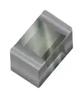


GG0402051R5L2P
TVS DIODE, BIDIR, 5V, 0402
- Manufacturer: KYOCERA AVX
- Product type: TVS Diodes
- Product Range:GiGuard Series; TVS Polarity:Bidirectional; Reverse Standoff Voltage:5V; Clamping Voltage Max:20V; Diode Case Style:0402; No. of Pins:2Pins; Minimum Breakdown 56AJ0588
- No. of Pins: 2Pins
- Qualification: -
| Delivery and price | |
|---|---|
| Units per pack | 100 |
| Price | 0.12 € |
| Current stock | 10+ |
| Lead time | 30 days |
**GiGuard[®] - ESD Protection for High Speed Circuits AVX Bi-directional Leadless Transient Voltage Suppressor Diodes Provid ESD Protection for High Speed Communication and Data Lines**

## **GENERAL DESCRIPTION**

Utilizing the latest in TVS Technology combined with a unique leadless package, the new GiGuard series of ESD Suppression Diodes offers Clamping Voltages below 12v and cap values as low as 0.3pfd. This combination of excellence both protects sensitive ICs during ESD events and preserves the integrity of the protected high speed signals. The AVX GG[®] series fits perfectly onto the same PCB solder pads as standard EIA 0201/0402/0603 components.

The GG[®] series complies with IEC 61000-4-2(ESD), Level 4+ (±20kV air, ±20kV contact discharge), IEC 61000-4-4 (electrical fast transient -EFT) (20A, 5/50 ns), very fast charged device model (CDM) ESD and cable discharge event (CDE).

## **APPLICATIONS**

- USB 2.0/3.0

- Tablets/Cell Phones Touch Screens

- Network Communications

- Gigabyte Ethernet

- High Def Multimedia Interface (HDMI)

## **FEATURES**

- Low Capacitance (.3pF to 17pF typ)

- Low Vc (<12v @ 1a)

- Bi-Directional protection

- Leadless 0201/0402 case size

- -55ºC ~ 125ºC Operating Range

## **CIRCUIT DIAGRAM**

- Mobile Phone Touchscreen

## **HOW TO ORDER**

## **GG 0201 05 100 N 2 P**

## **Series**

## **Case Size**

0201 0402 0603

## **Voltage Rating**

03 = 3.3V 07 = 7.0V 05 = 5.0V 12 = 12V 06 = 6.5V

## **Nominal Cap**

0R3 = 0.3pF 100 = 10pF 2R5 = 2.5pF 170 = 17pF 5R0 = 5.0pF

## **Finsih**

P = 100% Tin **Packaging**

2  = 7" Reel 0201   = 15K/Reel 0402 = 10K/Reel 0603 = 5K/Reel

## **Cap Tolerance**

4 = ±2pF C = ±.25pF N = ±30% M = ±20% L = min 0.5pf - max 2.5pf

## **CHARACTERISTIC TEST DESCRIPTION**

|**Characteristic Test Description**|**Symbol**|**Units**|
|---|---|---|
|Nominal Reverse Working Voltage|Vwrm|V|
|Reverse Min. Breakdown Voltage @ 1ma|Vbr|V|
|Reverse Leakage Current @Vwrm|IL|ua|
|Peak Pulse Power (tp=8x20us)|Ppp|W|
|Peak Pulse Current (tp=8x20us)|Ipp|A|
|ESD Rating - Air (150pf, 330Ω network)|Vair|KV|
|ESD Rating - Contact (150pf, 330Ω network)|Vcon|KV|


|**Characteristic Test Description**|**Symbol**|**Units**|
|---|---|---|
|Max Clamp Voltage @ Ipp = 16a|Vc16a|V|
|Max ESD Clamp Voltage @ 8KV|Vc8k|V|
|Max Clamp Voltage @ Ipp = 1a|Vc|V|
|Max Clamp Voltage @ Ipp|VcIpp|V|
|Nominal Capacitance (Vr=0v, f=1Mhz)|Cnom|pF|
|Allowable Capacitance Range|Cap (pF)|min-max|


The Important Information/Disclaimer is incorporated in the catalog where these specifications came from or available online at www.avx.com/disclaimer/ by reference and should be reviewed in full before placing any order.

1

112820

## **GiGuard[®] - ESD Protection for High Speed Circuits**

## **AVX Bi-directional Leadless Transient Voltage Suppressor Diodes Provid ESD Protection for High SPeed Communication and Data Lines**

## **GENERAL ELECTRICAL CHARACTERISTICS**

|**AVX Part Number**<br>~~Ge~~|**Vrwv**<br>**(V)**<br>~~Ge~~|**Cnom**<br>**(pF)**<br>~~Ge~~|**Cap Min**<br>**(pf)**<br>~~GeGe~~|**Cap**<br>**Max**<br>**(pF)**<br>~~GeGe~~|**Vbr Min**<br>**(V)**<br>~~GG~~|**IL**<br>**(µa)**<br>~~GG~~|**Vc (@Ipp=1a,**<br>**tp=8x20ns)**<br>**(V)**<br>~~GG~~|**Ipp (A)**<br>~~GG~~|**Vc (@Ipp,**<br>**tp=8x20ns)**<br>**(V)**<br>~~GG~~|**Ppp**<br>**(W)**<br>~~OO~~|**Vair**<br>**(KV)**|**Vcon**<br>**(KV)**|**Vc**<br>**(@8KV)**<br>**(V)**|**Pack QTY**|
|---|---|---|---|---|---|---|---|---|---|---|---|---|---|---|
|GG020103100N2P<br>~~Ge~~<br>~~Ge~~|3.3<br>~~Ge~~<br>~~Ge~~|10.0<br>~~Ge~~<br>~~Ge~~|7<br>~~GeGe~~<br>~~GG~~|13<br>~~GeGe~~<br>~~GG~~|4.0<br>~~GG~~<br>~~GG~~|<0 .1<br>~~GG~~<br>~~GG~~|≤6<br>~~GG~~<br>~~G(R~~|7<br>~~GG~~<br>~~G(R~~|≤10<br>~~GG~~<br>~~G(R~~|70.0<br>~~OO~~<br>~~OO~~|±20<br>~~OO~~|±20<br>~~OO~~|≤12|15000|
|GG020105100N2P<br>~~Ge~~<br>~~Ge~~<br>~~po~~<br>~~CL~~|5.0<br>~~Ge~~<br>~~Ge~~<br>~~CL~~|10.0<br>~~Ge~~<br>~~Ge~~|7<br>~~GeGe~~<br>~~GG~~|13.0<br>~~GeGe~~<br>~~GG~~|5.5<br>~~GG~~<br>~~GG~~|<0 .1<br>~~GG~~<br>~~GG~~|≤8<br>~~GG~~<br>~~G(R~~|6<br>~~GG~~<br>~~G(R~~|≤12<br>~~GG~~<br>~~G(R~~|60.0<br>~~OO~~<br>~~OO~~|±20<br>~~OO~~|±20<br>~~OO~~|≤12|15000|
|GG0201052R542P<br>~~Ge~~<br>~~po~~<br>~~CL~~<br>~~prceC~~|5.0<br>~~Ge~~<br>~~CL~~<br>~~eC~~|2.5<br>~~Ge~~<br>~~eC~~|0.5<br>~~GG~~<br>~~eC~~|4.5<br>~~GG ~~<br>~~eC~~|6.7<br> ~~GG~~<br>~~eC~~|<0 .1<br>~~GG~~<br>~~eC~~|≤12<br>~~G(R~~<br>~~eC~~|3<br>~~G(R~~<br>~~eC~~|≤15<br>~~G(R~~<br>~~eC~~|46.0<br>~~OO ~~<br>~~eC~~|±20<br> ~~OO~~<br>~~eC~~|±15<br>~~OO~~<br>~~eC~~|≤16<br>~~eC~~|15000<br>~~eC~~|
|GG040203100N2P<br>~~po~~<br>~~CL~~<br>~~prceC~~<br>~~re~~|3.3<br>~~CL~~<br>~~eC~~|10.0<br>~~eC~~|7<br>~~eC~~|13<br>~~eC~~<br>~~Ge~~|4.0<br>~~eC~~<br>~~GG~~|<0 .1<br>~~eC~~<br>~~GG~~|≤6<br>~~eC~~<br>~~GG~~|8<br>~~eC~~<br>~~GG~~|≤10<br>~~eC~~<br>~~GG~~|80.0<br>~~eC~~<br>~~OO~~|±30<br>~~eC~~<br>~~OO~~|±30<br>~~eC~~|≤10<br>~~eC~~|10000<br>~~eC~~|
|GG0402052R542P<br>~~prceC~~<br>~~eG~~<br>~~re~~<br>~~po~~|5.0<br>~~eC~~<br>~~eG~~<br>|2.5<br>~~eC~~<br>~~eG~~<br>|0.5<br>~~eC~~<br>~~eG~~<br>|4.5<br>~~eC~~<br>~~eG~~<br>~~Ge~~|5.5<br>~~eC~~<br>~~eG~~<br>~~GG~~|<0 .1<br>~~eC~~<br>~~eG~~<br>~~GG~~|≤12<br>~~eC~~<br>~~eG~~<br>~~GG~~|3<br>~~eC~~<br>~~eG~~<br>~~GG~~|≤15.5<br>~~eC~~<br>~~eG~~<br>~~GG~~|46.0<br>~~eC~~<br>~~eG~~<br>~~OO~~<br>~~OO~~|±15<br>~~eC~~<br>~~eG~~<br>~~OO~~<br>~~OO~~|±15<br>~~eC~~<br>~~eG~~<br>~~OO~~|≤16<br>~~eC~~<br>~~eG~~<br>~~OO~~|10000<br>~~eC~~<br>~~eG~~|
|GG0402055R042P<br>~~eG~~<br>~~re~~<br>~~po~~|5.0<br>~~eG~~<br>|5.0<br>~~eG~~<br>~~GG~~<br>|3<br>~~eG~~<br>~~GG~~<br>|7.0<br>~~eG~~<br>~~Ge~~<br>~~GG~~|5.2<br>~~eG~~<br>~~GG~~<br>~~GG (QO~~|<0 .1<br>~~eG~~<br>~~GG~~<br>~~(QO~~|≤12<br>~~eG~~<br>~~GG~~<br>~~(QO~~|4<br>~~eG~~<br>~~GG~~<br>~~(QO~~|≤16<br>~~eG~~<br>~~GG~~<br>~~(QO~~|60.0<br>~~eG~~<br>~~OO~~<br>~~(QO~~<br>~~OO~~|±15<br>~~eG~~<br>~~OO~~<br>~~(QO~~<br>~~OO~~|±15<br>~~eG~~<br>~~(QO~~<br>~~OO~~|≤15<br>~~eG~~<br>~~(QO~~<br>~~OO~~|10000<br>~~eG~~<br>~~(QO~~|
|GG040205100N2P<br>~~re~~<br>~~poLT~~<br>~~Pp~~|5.0<br>~~LT~~<br>|10.0<br>~~LT~~<br>|7<br>~~LT~~<br>|13.0<br>~~Ge~~<br>|5.5<br>~~GG~~<br>|<0 .1<br>~~GG ~~|≤8<br> ~~GG~~|8<br>~~GG~~|≤12<br>~~GG~~|96.0<br>~~OO~~<br>~~OO~~|±25<br>~~OO~~<br>~~OO~~|±25<br>~~OO~~|≤12<br>~~OO~~|10000|
|GG040205170N2P<br>~~po LT~~<br>~~Ppse~~|5.0<br>~~LT~~<br>~~se~~|17.0<br>~~LT~~<br>~~Gn~~|11.9<br>~~LT~~<br>~~GeGs~~|22.0<br>~~GeGs~~|5.1<br>~~GN~~|<0 .1|≤6.5<br>~~S(O~~|8<br>~~S(O~~|≤10<br>~~(OO~~|80.0<br>~~OO ~~<br>~~(OO~~|±30<br> ~~OO ~~|±30<br> ~~OO~~|≤12<br>~~OO~~|10000|
|GG040205320M2P<br> ~~LT~~<br>~~Ppse~~|5.0<br>~~LT~~<br>~~se~~|32.0<br>~~LT~~<br>~~Gn~~|25.6<br>~~LT~~<br>~~GeGs~~|38.4<br>~~GeGs~~|6<br>~~GN~~|<0 .1|≤7<br>~~S(O~~|18<br>~~S(O~~|≤11<br>~~(OO~~|200.0<br>~~(OO~~|±30|±30|≤11|10000|
|GG040207100N2P<br>~~se~~<br>~~pC~~<br>~~po~~|7.0<br>~~se ~~<br>~~pC~~<br>|10.0<br> ~~Gn ~~<br>~~pC~~<br>|7<br> ~~GeGs~~<br>~~pC~~<br>|13<br>~~GeGs ~~<br>~~pC~~<br>|9.0<br> ~~GN~~<br>~~pC~~<br>|<0 .1<br>~~pC~~<br>|≤10<br>~~S(O~~<br>~~pC~~<br>|6<br>~~S(O ~~<br>~~pC~~<br>|≤12<br> ~~(OO~~<br>~~pC~~<br>|72.0<br>~~(OO~~<br>~~pC~~<br>|±30<br>~~pC~~<br>|±30<br>~~pC~~<br>|≤13<br>~~pC~~<br>|10000<br>~~pC~~<br>|
|GG0402126R042P<br>~~potl~~<br>~~po~~<br>~~tl~~|12.0<br>~~tl~~<br>~~tl~~|6.0<br>~~tl~~|4<br>~~tl~~|8<br>~~tl~~|18.0<br>~~tl~~|<0 .1<br>~~tl~~|≤18<br>~~tl~~|6<br>~~tl~~|≤22<br>~~tl~~|130.0<br>~~tl~~|±25<br>~~tl~~|±25<br>~~tl~~|≤22<br>~~tl~~|10000<br>~~tl~~|
|GG060303100N2P<br>~~po~~<br>~~po~~<br>~~tl~~<br>~~po~~|3.3<br><br>~~tl~~<br>~~po~~|10.0<br><br>~~po~~|7<br>|13<br>|3.4<br>|<0 .1<br>|≤6<br>|8<br>|≤10<br>|80.0<br>|±30<br>|±30<br>|≤10<br>|5000<br>|
|GG0603052R542P<br>~~po~~<br>~~tl~~<br>~~po~~<br>~~po~~|5.0<br>~~tl~~<br>~~po~~<br>~~po~~|2.5<br>~~po~~|0.5|4.5|6.7|<0 .1|≤12|3|≤15|45.0|±15|±15|≤16|5000|
|GG060305100N2P<br>~~po~~<br>~~po~~|5.0<br>~~po~~<br>~~po~~|10.0<br>~~po~~|7|13|7.5|<0 .1|≤8|8|≤12|96.0|±25|±25|≤12|5000|


## **HIGH POWER ELECTRICAL CHARACTERISTICS**

|**AVX Part Number**|**Vrwv**<br>**(V)**|**Cnom**<br>**(pF)**|**Cap Min**<br>**(pf)**|**Cap**<br>**Max**<br>**(pF)**|**Vbr Min**<br>**(V)**|**IL**<br>**(µa)**|**Vc (@Ipp=1a,**<br>**tp=8x20ns)**<br>**(V)**|**Ipp (A)**|**Vc (@Ipp,**<br>**tp=8x20ns)**<br>**(V)**|**Ppp**<br>**(W)**|**Vair**<br>**(KV)**|**Vcon**<br>**(KV)**|**Vc**<br>**(@8KV)**<br>**(V)**|**Pack QTY**|
|---|---|---|---|---|---|---|---|---|---|---|---|---|---|---|
|GG0402050R8L2P|5.0|0.8|0.5|2.5|8.0|<0 .1|≤9|7|≤15|100|±30|±30|≤13|10000|
|GG0402051R5L2P|5.0|1.5|0.5|2.5|8.0|<0 .1|≤9|15|≤20|300|±30|±30|≤12|10000|


## **LOW CAP ELECTRICAL CHARACTERISTICS**

|**AVX Part Number**<br>~~po~~|**Vrwv**<br>**(V)**|**Cnom**<br>**(pF)**|**Cap Min**<br>**(pf)**|**Cap**<br>**Max**<br>**(pF)**|**Vbr Min**<br>**(V)**|**IL**<br>**(µa)**|**Vc (@Ipp=1a,**<br>**tp=8x20ns)**<br>**(V)**|**Ipp (A)**|**Vc (@Ipp,**<br>**tp=8x20ns)**<br>**(V)**|**Ppp**<br>**(W)**|**Vair**<br>**(KV)**|**Vcon**<br>**(KV)**|**Vc**<br>**(@8KV)**<br>**(V)**|**Pack QTY**|
|---|---|---|---|---|---|---|---|---|---|---|---|---|---|---|
|GG0201050R3C2P<br>~~po~~<br>~~Pp~~<br>~~Cl~~|5.0<br>~~Cl~~|0.3|0.15|0.55|8.0|<0 .1|≤15|3|≤20|60.0|±20|±20|≤30|15000|
|GG0402050R4C2P<br>~~po~~<br>~~Pp~~<br>~~Cl~~<br>~~rs~~|5.0<br>~~Cl~~<br>~~Ge~~|0.35<br>~~Ge~~|0.15<br>~~GeGs~~|0.65<br>~~GeGs~~|8.5<br>~~GG~~|<0 .1<br>~~GG~~|≤10<br>~~(GO~~|4<br>~~(GO~~|≤12<br>~~(GO~~|60.0<br>~~OO~~|±20|±20|≤15|10000|
|GG0402050R3C2P<br>~~Pp~~<br>~~Cl~~<br>~~rs~~|5.0<br>~~Cl~~<br>~~Ge~~|0.3<br>~~Ge~~|0.15<br>~~GeGs~~|0.55<br>~~GeGs~~|7.0<br>~~GG~~|<0 .1<br>~~GG~~|≤12<br>~~(GO~~|3<br>~~(GO~~|≤15.5<br>~~(GO~~|54.0<br>~~OO~~|±20|±20|≤30|10000|
|GG0402060R3C2P<br>~~rs ~~<br>~~pC~~|6.5<br> ~~Ge~~<br>~~pC~~|0.3<br>~~Ge~~<br>~~pC~~|0.15<br>~~GeGs~~<br>~~pC~~|0.55<br>~~GeGs~~<br>~~pC~~|7.0<br>~~GG~~<br>~~pC~~|<0.1<br>~~GG~~<br>~~pC~~|≤12<br>~~(GO~~<br>~~pC~~|3<br>~~(GO~~<br>~~pC~~|≤15.5<br>~~(GO~~<br>~~pC~~|54.0<br>~~OO~~<br>~~pC~~|±20<br>~~pC~~|±20<br>~~pC~~|≤30<br>~~pC~~|10000<br>~~pC~~|


The Important Information/Disclaimer is incorporated in the catalog where these specifications came from or available online at www.avx.com/disclaimer/ by reference and should be reviewed in full before placing any order.

2

112820

## **GiGuard[®] - ESD Protection for High Speed Circuits Characteristic Curves - Types**

## **GG020105100N2P (10PF)**

## **GG0402060R3C2P (0.3PF)**

The Important Information/Disclaimer is incorporated in the catalog where these specifications came from or available online at www.avx.com/disclaimer/ by reference and should be reviewed in full before placing any order.

3

## **GiGuard[®] - ESD Protection for High Speed Circuits Characteristic Curves - Types**

## **GG0402052R542P (2.5PF)**

## **GG0402055R042P (5.0PF)**

The Important Information/Disclaimer is incorporated in the catalog where these specifications came from or available online at www.avx.com/disclaimer/ by reference and should be reviewed in full before placing any order.

4

101320

## **GiGuard[®] - ESD Protection for High Speed Circuits Characteristic Curves - Types**

## **GGS040205100N2P (10PF)**

## **GG040205170N2P (17PF)**

The Important Information/Disclaimer is incorporated in the catalog where these specifications came from or available online at www.avx.com/disclaimer/ by reference and should be reviewed in full before placing any order.

5

101320

## **GiGuard[®] - ESD Protection for High Speed Circuits**

## **TEMPERATURE DERATING**

## **DIMENSIONS**

**==> picture [141 x 81] intentionally omitted <==**

**----- Start of picture text -----**<br>
L<br>— t<br>T<br>T L) s tn<br>**----- End of picture text -----**<br>


mm (inches)

**==> picture [249 x 72] intentionally omitted <==**

**----- Start of picture text -----**<br>
||||||
|---|---|---|---|---|
|Size|Length (L)|Width (W)|Thickness (T)|Termination (t)|
|0.60 ± 0.03|0.30 ± 0.03|0.30 ± 0.03|0.15 ± 0.05|
|0201|
|(0.024 ± 0.001)|(0.012 ± 0.001)|(0.012 ± 0.001)|(0.006 ± 0.002)|
|1.00 ± 0.05|0.60 ± 0.05|0.50 ± 0.05|0.20 ± 0.05|
|0402|
|(0.039 ± 0.002)|(0.024 ± 0.002)|(0.020 ± 0.002)|(0.008 ± 0.002)|
|1.60 ± 0.10|0.80 ± 0.10|0.60 ± 0.10|0.30 ± 0.05|
|0603|
|(0.063 ± 0.004)|(0.031 ± 0.004)|(0.024 ± 0.004)|(0.012 ± 0.002)|

**----- End of picture text -----**<br>


## **RECOMMENDED SOLDER REFLOW PROFILES**

## **RECOMMENDED REFLOW SOLDER PAD**

**==> picture [249 x 190] intentionally omitted <==**

**----- Start of picture text -----**<br>
||||||
|---|---|---|---|---|
|D|
|-|+|
|A|
|C|B|
|A|
|_|
|mm (inches(inchesinches)|
|Size|A|B|C|D|
|0.25 ± 0.05|0.30 ± 0.05|0.80 ± 0.15|0.275 ± 0.025|
|0201|
|(0.010 ± 0.002)|(0.012 ± 0.002)|(0.031 ± 0.006)|(0.011 ± 0.001)|
|0.61 ± 0.05|0.51 ± 0.05|1.70 ± 0.05|0.51 ± 0.05|
|0402|
|(0.024 ± 0.002)|(0.020 ± 0.002)|(0.067 ± 0.002)|(0.020 ± 0.002)|
|0.30 ± 0.05|1.0 ± 0.1|1.6 ± 0.1|0.6 ± 0.1|
|0603|
|(0.012 ± 0.002)|(0.039 ± 0.004)|(0.063 ± 0.004)|(0.024 ± 0.004)|

**----- End of picture text -----**<br>


mm (inches(inchesinches)

Recommended Reflow Profiles

**==> picture [259 x 137] intentionally omitted <==**

**----- Start of picture text -----**<br>
275<br>Pb Free Recommended<br>250 Pb Free Max with care<br>225 t= Sn Pb Recommended e ye<br>_ PC R<br>200<br>175 TT] EA S SS TT<br>150 BEEE DS2 Ze LR AT<br>125 | RT | | aN<br>100 (|e LTE EN S<br>PIA TIT TT Te eee eT tT | NGS<br>75 2 4ERRR<br>50<br>A Tt ttt te ee ee Tt TY<br>25 A REER<br>02 04 06 08 0 100 120 140 160 180 200 220 240 260 280 300 320 340 360 380 400 420<br>Time / secs<br>Component Temperature / °C<br>**----- End of picture text -----**<br>


Hand Soldering Cautions

In hand soldering of the Devices. Large temperature gradient between preheated the Devices and the tip of soldering iron may cause electrical failures and mechanical damages such as cracking or breaking of the devices. The soldering shall be carefully controlled and carried out so that the temperature gradient is kept minimum with following recommended conditions for hand soldering.

## **RECOMMENDED SOLDERING CONDITION 1**

1. Solder: **0.12~0.18mm** Thread solder (Sn96.5:Ag3.5) with soldering flux in the core Rosin-based and non-activated flux is recommended.

2. Preheating: The Devices shall be preheated so that Temperature Gradient between the devices and the tip of soldering iron is 150° or below.

3. Soldering Iron: Rated Power of 20w max with 3mm soldering tip in diameter. Temperature of soldering iron tip **300ºCmax, 3-5sec** (The required amount of solder shall be melted in advance on the soldering tip.)

4. Cooling: After soldering. The Devices shall be cooled gradually at room ambient temperature.

## **RECOMMENDED SOLDERING CONDITION 2 – WITHOUT PREHEATING**

1. Temperature of soldering iron tip 300°C max, 3-5sec.

2. Solder iron tip shall not directly touch to Devices.

3. Solder iron tip shall be fully preheated before soldering while soldering iron tip to the external electrode of Devices.

The Important Information/Disclaimer is incorporated in the catalog where these specifications came from or available online at www.avx.com/disclaimer/ by reference and should be reviewed in full before placing any order.

6

012821

## **GiGuard[®] - ESD Protection for High Speed Circuits**

## **PACKAGING SPECIFICATION**

- Carrier tape and transparent cover tape should be heat-sealed to carry the products, and the reel should be used to reel the carrier tape.

- The adhesion of the heat-sealed cover tape shall be 25~60 grams with nominal of 40 grams.

- Both the head and the end portion of the taping shall be empty for reel package and SMT auto-pickup machine. And a normal paper tape shall be connected in the head of taping for the operator to handle.

mm (inches)

|**Case**<br>**Size**|**A0**<br>**±0.05**<br>**(0.002)**|**B0**<br>**±0.05**<br>**(0.002)**|**K0**<br>**±0.05**<br>**(0.002)**|**D**<br>**+0.10 (0.004)**<br>**-0.05 (0.002)**|**P**<br>**±0.10**<br>**(0.004)**|**P2**<br>**±0.10**<br>**(0.004)**|**P0**<br>**±0.10**<br>**(0.004)**|**W**<br>**±0.10**<br>**(0.004)**|**E**<br>**±0.10**<br>**(0.004)**|**F**<br>**±0.05**<br>**(0.002)**|**Qty**|
|---|---|---|---|---|---|---|---|---|---|---|---|
|0201|0.37<br>(0.015)|0.67<br>(0.026)|0.50<br>(0.020)|1.50<br>(0.059)|2.00<br>(0.079)|2.00<br>(0.079)|4.00<br>(0.157)|8.00<br>(0.315)|1.75<br>(0.069)|3.50<br>(0.138)|15K|
|0402|0.70<br>(0.028)|1.12<br>(0.044)|0.60<br>(0.024)|1.55<br>(0.061)|2.00<br>(0.079)|2.00<br>(0.079)|4.00<br>(0.157)|8.00<br>(0.315)|1.75<br>(0.069)|3.50<br>(0.138)|10k|
|0603|1.00<br>(0.039)|1.80<br>(0.071)|0.70<br>(0.028)|1.50<br>(0.059)|4.00<br>(0.157)|2.00<br>(0.079)|4.0<br>(0.157)|8.00<br>(0.315)|1.75<br>(0.069)|3.50<br>(0.138)|5K|


## **REEL DIMENSIONS**

mm (inches)

|**Reel Size**|**A**|**B**|**C**|**D**|**E**|**W**|**W1**|
|---|---|---|---|---|---|---|---|
|7"|178.0 ± 1.0<br>(7.008 ± 0.039)|60.0 ± 0.5<br>(2.362 ± 0.020)|13.0 ± 0.2<br>(0.512 ± 0.008)|21.0 ± 0.2<br>(0.827 ± 0.008)|2.0 ± 0.5<br>(0.079 ± 0.020)|9.0 ± 0.50<br>(0.354 ± 0.020)|1.5 ± 0.15<br>(0.059 ± 0.006)|


The Important Information/Disclaimer is incorporated in the catalog where these specifications came from or available online at www.avx.com/disclaimer/ by reference and should be reviewed in full before placing any order.

7

012821
Updated at April 15, 2026
KYOCERA AVX is a globally recognized leader in the design, development, and manufacturing of advanced electronic components. For over 50 years, the company has provided innovative solutions across the automotive, industrial, medical, military, consumer electronics, and communications markets. Supported by an extensive international network of research and production facilities, KYOCERA AVX is renowned for delivering highly reliable components that meet the stringent demands of modern engineering. The manufacturer's extensive portfolio is strongly anchored in high-performance passive components, with a particular emphasis on advanced capacitive solutions. Their offering features a comprehensive selection of polymer capacitors, RF capacitors, and supercapacitors engineered for demanding power and high-frequency requirements. This core lineup is further supported by a variety of film and aluminium electrolytic capacitors, alongside precision power inductors. Beyond passive components, KYOCERA AVX excels in robust circuit protection and discrete semiconductors. Their expertise in transient voltage suppression is demonstrated by a wide array of TVS varistors and TVS diodes, complemented by temperature-sensing NTC thermistors and reliable Schottky diodes. The product ecosystem is completed by precision timing devices, including crystals and resonators, as well as specialized RF antennas, providing engineers with a versatile and dependable foundation for next-generation technology.
About Novapart
Novapart is a B2B electronic component broker specialising in stock shortages and cost reduction. We source hard-to-find parts and identify compliant alternatives across a catalogue of 420,000+ components from 500+ manufacturers.
Learn more →Stock Shortage Specialist
When a component is unavailable, discontinued or has an unacceptable lead time, we tap into our network of vetted European and Asian distributors to source what you need — without compromising on quality or traceability.
Request a quote →Compliant Alternatives
We identify pin-to-pin, electrically equivalent substitutes that meet the same certifications (RoHS, AEC-Q100, REACH) as your original specification — validated against datasheets, not just part numbers. Often at a lower cost.
BOM Analysis service →