
Image not available
Illustrative purposes only

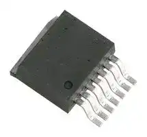
GC05MPS33J
Silicon Carbide Schottky Diode, MPS Series, Single, 3.3 kV, 11 A, 42 nC, TO-263 (D2PAK)
⚠️ Reference pricing provided. In case of supply shortages, we will connect you with our trusted procurement partners to ensure your project's continuity.
- Manufacturer: GENESIC
- Product type: Silicon Carbide Schottky Diodes
- Available until stocks are exhausted
- SVHC: No SVHC (17-Dec-2015)
- No. of Pins: 7 Pin
- Product Range: MPS Series
- Qualification: -
- Diode Mounting: Surface Mount
- Diode Case Style: TO-263 (D2PAK)
- Diode Configuration: Single
- Average Forward Current: 11A
- Total Capacitive Charge: 42nC
- Operating Temperature Max: 175°C
- Repetitive Peak Reverse Voltage: 3.3kV
| Delivery and price | |
|---|---|
| Units per pack | 100 |
| Price | 15.47 € |
| Current stock | 100+ |
| Lead time | 30 days |
Datasheet

**GC05MPS33J 3300V 5A SiC Schottky MPS™ Diode**

**TM**

**Silicon Carbide Schottky Diode VRRM = 3300 V IF (TC = 157°C) = 5 A QC = 42 nC** |

**==> picture [536 x 520] intentionally omitted <==**

**----- Start of picture text -----**<br>
|||||||
|---|---|---|---|---|---|
|Features|Package|
|•  Enhanced Surge and Avalanche Robustness|
|Case|
|•  Low VF for High Temperature Operation|
|•  Superior Figure of Merit QC/IF|
|•  Low Thermal Resistance|RoHS|
|•  Low Reverse Leakage Current|
|•  Temperature Independent Fast Switching|
|•  Positive Temperature Coefficient of VF|
|•  High dV/dt Ruggedness|
|TO-263-7|K|A|REACH|
|a|[|4|
|Advantages|Applications|
|•  High System Reliability|•  High Voltage Sensing|
|•  Optimal Price Performance|•  Oil Drilling|
|•  Improved System Efficiency|•  Geothermal Instrumentation|
|•  Reduced Cooling Requirements|•  High Voltage Multipliers|
|•  Increased System Power Density|•  High Frequency Rectifiers|
|•  Zero Reverse Recovery Current|•  High Voltage Switching|
|•  Easy to Parallel without Thermal Runaway|•  Pulsed Power|
|•  Enables Extremely Fast Switching|
|—|
|Absolute Maximum Ratings|(At TC = 25°C Unless Otherwise Stated)|
|Parameter|Symbol|Conditions|Values|Unit|Note|
|Repetitive Peak Reverse Voltage|VRRM|3300|V|
|TC = 100°C, D = 1|11|
|Continuous Forward Current|I  F|TC = 135°C, D = 1|8|A|Fig. 4|
|TC = 157°C, D = 1|5|
|Non-Repetitive Peak Forward Surge Current, Half Sine|TC = 25°C, tP = 10 ms|50|
|Wave|IF,SM|TC = 150°C, tP = 10 ms|40|A|
|TC = 25°C, tP = 10 ms|30|
|Repetitive Peak Forward Surge Current, Half Sine Wave|IF,RM|A|
|TC = 150°C, tP = 10 ms|21|
|Non-Repetitive Peak Forward Surge Current|IF,MAX|TC = 25°C, tP = 10 µs|250|A|
|i2t Value|∫i2dt|TC = 25°C, tP = 10 ms|12|A s 2|
|Non-Repetitive Avalanche Energy|EAS|L = 8 mH, IAS = 5 A|100|mJ|
|Diode Ruggedness|dV/dt|VR = 0 ~ 2640 V|200|V/ns|
|Power Dissipation|PTOT|TC = 25°C|178|W|Fig. 3|
|Operating and Storage Temperature|T  , Tj|stg|-55 to 175|°C|

**----- End of picture text -----**<br>


**Latest Version at: www.genesicsemi.com/sic-schottky-mps/GC05MPS33J/GC05MPS33J.pdf**

**Page 1 of 7**

**Rev 22/Apr**

**GC05MPS33J 3300V 5A SiC Schottky MPS™ Diode**

**TM**

## **Electrical Characteristics**

**==> picture [536 x 158] intentionally omitted <==**

**----- Start of picture text -----**<br>
Values<br>Parameter  Symbol  Conditions  Unit  Note<br>Min.  Typ.  Max.<br>I  = 5 A, T  = 25°C F j 2.4  3.0<br>Diode Forward Voltage  V  F V  Fig. 1<br>I  = 5 A, T  = 175°C F j 4.5<br>VR = 3300 V, T  = 25°C j 1  50<br>Reverse Current  IR µA  Fig. 2<br>VR = 3300 V, T  = 175°C j 10<br>VR = 1500 V  39<br>Total Capacitive Charge  QC nC  Fig. 7<br>I  ≤ IF F,MAX VR = 1700 V  42<br>dI /dt = 200 A/µs F VR = 1500 V<br>Switching Time  tS < 10  ns<br>VR = 1700 V<br>VR = 1 V, f = 1MHz  337<br>Total Capacitance  C  pF  Fig. 6<br>VR = 1700 V, f = 1MHz  14<br>**----- End of picture text -----**<br>


**==> picture [544 x 81] intentionally omitted <==**

**----- Start of picture text -----**<br>
Thermal/Package Characteristics<br>Values<br>Parameter  Symbol  Conditions  Unit  Note<br>Min.  Typ.  Max.<br>Thermal Resistance, Junction - Case  RthJC 0.84  °C/W  Fig. 9<br>Weight  WT 1.45  g<br>**----- End of picture text -----**<br>


**==> picture [60 x 46] intentionally omitted <==**

**Latest Version at: www.genesicsemi.com/sic-schottky-mps/GC05MPS33J/GC05MPS33J.pdf**

**Page 2 of 7**

**Rev 22/Apr**

**GC05MPS33J 3300V 5A SiC Schottky MPS™ Diode**

**TM**

**Figure 1: Typical Forward Characteristics**

IF = f(VF,T); tj P = 250 µs

**Figure 3: Power Derating Curves**

**==> picture [97 x 12] intentionally omitted <==**

**----- Start of picture text -----**<br>
PTOT = f(TC); T = 175°C j<br>**----- End of picture text -----**<br>


**Figure 2: Typical Reverse Characteristics**

**==> picture [46 x 12] intentionally omitted <==**

**----- Start of picture text -----**<br>
IR = f(VR,T)j<br>**----- End of picture text -----**<br>


**Figure 4: Current Derating Curves (Typical VF)**

**==> picture [169 x 12] intentionally omitted <==**

**----- Start of picture text -----**<br>
IF = f(TC); D = tP/T; T ≤ 175°C; fj SW > 10kHz<br>**----- End of picture text -----**<br>


**Latest Version at: www.genesicsemi.com/sic-schottky-mps/GC05MPS33J/GC05MPS33J.pdf**

**Page 3 of 7**

**Rev 22/Apr**

**GC05MPS33J 3300V 5A SiC Schottky MPS™ Diode**

**==> picture [5 x 4] intentionally omitted <==**

**----- Start of picture text -----**<br>
TM<br>**----- End of picture text -----**<br>


**==> picture [225 x 14] intentionally omitted <==**

**----- Start of picture text -----**<br>
Figure 5: Current Derating Curves (Maximum VF)<br>**----- End of picture text -----**<br>


**==> picture [170 x 12] intentionally omitted <==**

**----- Start of picture text -----**<br>
IF = f(TC); D = tP/T; T ≤ 175°C; fj SW > 10kHz<br>**----- End of picture text -----**<br>


**Figure 7: Typical Capacitive Charge vs Reverse Voltage Characteristics**

**==> picture [83 x 12] intentionally omitted <==**

**----- Start of picture text -----**<br>
QC = f(VR); f = 1MHz<br>**----- End of picture text -----**<br>


**Figure 6: Typical Junction Capacitance vs Reverse Voltage Characteristics**

**==> picture [78 x 12] intentionally omitted <==**

**----- Start of picture text -----**<br>
C = f(VR); f = 1MHz<br>**----- End of picture text -----**<br>


**Figure 8: Typical Capacitive Energy vs Reverse Voltage Characteristics**

**==> picture [82 x 12] intentionally omitted <==**

**----- Start of picture text -----**<br>
EC = f(VR); f = 1MHz<br>**----- End of picture text -----**<br>


**Latest Version at: www.genesicsemi.com/sic-schottky-mps/GC05MPS33J/GC05MPS33J.pdf**

**Page 4 of 7**

**Rev 22/Apr**

**GC05MPS33J 3300V 5A SiC Schottky MPS™ Diode**

**==> picture [5 x 4] intentionally omitted <==**

**----- Start of picture text -----**<br>
TM<br>**----- End of picture text -----**<br>


**Figure 9: Transient Thermal Impedance**

**==> picture [89 x 12] intentionally omitted <==**

**----- Start of picture text -----**<br>
Zth,jc = f(tP,D); D = tP/T<br>**----- End of picture text -----**<br>


**Figure 10: Forward Curve Model**

## **Forward Curve Model Equation:**

IF = (VF - VBI)/RDIFF (A) CO **Built-In Voltage (VBI):** VBI(T) = j m × T + j n (V) m = -0.00129 (V/°C) n = 1.0 (V)

**Differential Resistance (RDIFF):**

**==> picture [90 x 145] intentionally omitted <==**

**----- Start of picture text -----**<br>
1/RDIFF<br>a eee<br>VBI<br>Forward<br>IF = f(VF,T)j<br>**----- End of picture text -----**<br>


- RDIFF(T) = j a × Tj[2] + b × T + j c (Ω) a = 8.89e-06 (Ω/°C2) b = 0.00126 (Ω/°C) c = 0.207 (Ω)

**Forward Power Loss Equation:**

PLOSS = VBI(T) × Ij AVG + RDIFF(T) × Ij RMS[2]

**Latest Version at: www.genesicsemi.com/sic-schottky-mps/GC05MPS33J/GC05MPS33J.pdf**

**Page 5 of 7**

**Rev 22/Apr**

**GC05MPS33J 3300V 5A SiC Schottky MPS™ Diode**

**==> picture [5 x 4] intentionally omitted <==**

**----- Start of picture text -----**<br>
TM<br>**----- End of picture text -----**<br>


## **Package Dimensions**

## **TO-263-7 Package Outline**

## **Recommended Solder Pad Layout**

## **Package View**

**==> picture [409 x 134] intentionally omitted <==**

**----- Start of picture text -----**<br>
0.413(10.48)<br>0.130(3.3)<br>Case (K) Case (K)<br>0.249(6.32)<br>0.640(16.25)<br>0.0315(0.8)<br>J<br>NC A<br>0.126(3.2)<br>0.05(1.27)<br>**----- End of picture text -----**<br>


## **NOTE**

1. CONTROLLED DIMENSION IS INCH. DIMENSION IN BRACKET IS MILLIMETER.

2. DIMENSIONS DO NOT INCLUDE END FLASH, MOLD FLASH, MATERIAL PROTRUSIONS.

**Latest Version at: www.genesicsemi.com/sic-schottky-mps/GC05MPS33J/GC05MPS33J.pdf**

**Page 6 of 7**

**Rev 22/Apr**

**GC05MPS33J 3300V 5A SiC Schottky MPS™ Diode**

**==> picture [5 x 4] intentionally omitted <==**

**----- Start of picture text -----**<br>
TM<br>**----- End of picture text -----**<br>


## **Compliance**

## **RoHS Compliance**

The levels of RoHS restricted materials in this product are below the maximum concentration values (also referred to as the threshold limits) permitted for such substances, or are used in an exempted application, in accordance with EU Directive 2011/65/EC (RoHS 2), as adopted by EU member states on January 2, 2013 and amended on March 31, 2015 by EU Directive 2015/863. RoHS Declarations for this product can be obtained from your GeneSiC representative.

## **REACH Compliance**

REACH substances of high concern (SVHCs) information is available for this product. Since the European Chemical Agency (ECHA) has published notice of their intent to frequently revise the SVHC listing for the foreseeable future, please contact a GeneSiC representative to insure you get the most up-to-date REACH SVHC Declaration. REACH banned substance information (REACH Article 67) is also available upon request.

## **Disclaimer**

GeneSiC Semiconductor, Inc. reserves right to make changes to the product specifications and data in this document without notice. GeneSiC disclaims all and any warranty and liability arising out of use or application of any product. No license, express or implied to any intellectual property rights is granted by this document.

Unless otherwise expressly indicated, GeneSiC products are not designed, tested or authorized for use in life-saving, medical, aircraft navigation, communication, air traffic control and weapons systems, nor in applications where their failure may result in death, personal injury and/or property damage.

## **Related Links**

- SPICE Models: https://www.genesicsemi.com/sic-schottky-mps/GC05MPS33J/GC05MPS33J_SPICE.zip

- PLECS Models: https://www.genesicsemi.com/sic-schottky-mps/GC05MPS33J/GC05MPS33J_PLECS.zip

- CAD Models: https://www.genesicsemi.com/sic-schottky-mps/GC05MPS33J/GC05MPS33J_3D.zip

- Evaluation Boards: https://www.genesicsemi.com/technical-support

- Reliability: https://www.genesicsemi.com/reliability

- Compliance: https://www.genesicsemi.com/compliance

- Quality Manual: https://www.genesicsemi.com/quality

## **Revision History**

- Rev 22/Apr: Initial Release

**==> picture [86 x 86] intentionally omitted <==**

## **www.genesicsemi.com/sic-schottky-mps/**

**==> picture [90 x 78] intentionally omitted <==**

**Rev 22/Apr Copyright© 2022 GeneSiC Semiconductor Inc. All Rights Reserved.**

**Published by GeneSiC Semiconductor, Inc. 43670 Trade Center Place Suite 155, Dulles, VA 20166; USA Page 7 of 7**
Updated at April 22, 2026
About Novapart
Novapart is a B2B electronic component broker specialising in stock shortages and cost reduction. We source hard-to-find parts and identify compliant alternatives across a catalogue of 410,000+ components from 500+ manufacturers.
Learn more →Stock Shortage Specialist
When a component is unavailable, discontinued or has an unacceptable lead time, we tap into our network of vetted European and Asian distributors to source what you need — without compromising on quality or traceability.
Request a quote →Compliant Alternatives
We identify pin-to-pin, electrically equivalent substitutes that meet the same certifications (RoHS, AEC-Q100, REACH) as your original specification — validated against datasheets, not just part numbers. Often at a lower cost.
BOM Analysis service →