
Image not available
Illustrative purposes only

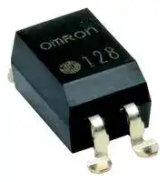
G3VM-201DY1(TR05)
MOSFET RELAY, SPST-NO, 0.25A, 200V, SMD
⚠️ Reference pricing provided. In case of supply shortages, we will connect you with our trusted procurement partners to ensure your project's continuity.
- Manufacturer: OMRON ELECTRONIC COMPONENTS
- Product type: MOSFET Solid State Relays
- ; MOSFET RELAY, SPST-NO, 0.25A, 200V, SMD; Contact Form:SPST-NO (1 Form A); Load Type:AC / DC; Load Voltage Max:200V; Load Current:250mA; MOSFET Relay Package Style:DIP-4; Relay Mo
- SVHC: No SVHC (17-Dec-2014)
- Load Type: AC / DC
- Contact Form: SPST-NO (1 Form A)
- Load Current: 250mA
- Product Range: G3VM Series
- Relay Mounting: Surface Mount
- Relay Terminals: Gull Wing
- Load Voltage Max: 200V
- Isolation Voltage: 5kV
- I/O Capacitance Typ: -
- On State Resistance Max: 8ohm
- MOSFET Relay Package Style: DIP-4
- Off State Leakage Current Max: -
| Delivery and price | |
|---|---|
| Units per pack | 250 |
| Price | 1.81 € |
| Current stock | 10+ |
| Lead time | 30 days |
Datasheet

**G3VM-@** AY **@** / **@** DY **@ MOS FET Relays    Small DIP4 package with High dielectric strength type**

## **Small DIP4 package with Dielectric Strength of 5,000 VAC between I/O**

- **Load voltage 40V/60V/200V/350V/400V/600V**

**==> picture [7 x 25] intentionally omitted <==**

**----- Start of picture text -----**<br>
D<br>I<br>P<br>**----- End of picture text -----**<br>


- **Standard type: Trigger LED forward current 3mA (max.)**

- **High sensitive type: Trigger LED forward current 2mA (max.)**

**==> picture [392 x 125] intentionally omitted <==**

**----- Start of picture text -----**<br>
G RoHS Compliant<br>3<br>V<br>Refer to " Common Precautions ".<br>M Note:<br>I<br>@<br>AY ■ Application Examples<br>@<br>/ • Electrical power unit • Security equipment • Medical equipment<br>@<br>• Test & measurement equipment • Industrial equipment<br>D<br>Y<br>@<br>**----- End of picture text -----**<br>


**Note:** The actual product is marked differently from the image shown here.

## ■ **Package (Unit : mm, Average)** ■ **Model Number Legend**

## **G3VM-** @ @ @ @ @

**==> picture [507 x 149] intentionally omitted <==**

**----- Start of picture text -----**<br>
1 2 3 4 5<br>1. Load Voltage 3. Package type 5. Other informations<br>4: 40V A: DIP4 pin PCB terminals When specifications overlap,<br>6: 60V D: DIP4 pin Surface- serial code is added in the<br>20: 200V mounting Terminals recorded order.<br>35: 350V 4. Additional functions<br>KS 40: 400V Y: Dielectric strength<br>60: 600V between I/O above<br>2. Contact form 2,500V type<br>Note:  The actual product is marked differently  1: 1a (SPST-NO)<br>from the image shown here.<br>3.65<br>3.65<br>4.58<br>6.4<br>4.58<br>6.4<br>**----- End of picture text -----**<br>


## ■ **Ordering Information**

Standard type **Packing/Tube Packing/Tape & reel Continuous Package Contact Load voltage load current Model Minimum Model Minimum type form (peak value)** * **(peak value)** * **PCB terminals Surface-mounting package Surface-mounting package** ~~L S—S~~ **Terminals quantity Terminals quantity** 40V 2000mA **G3VM-41AY1 G3VM-41DY1 G3VM-41DY1(TR05)** ~~a A es es es es~~ 60V 500mA **G3VM-61AY1 G3VM-61DY1** ~~|—iSY~~ **G3VM-61DY1(TR05)** 200V 250mA **G3VM-201AY1 G3VM-201DY1 G3VM-201DY1(TR05)** DIP4 1a 100 pcs. 500 pcs. 350V 100mA **G3VM-351AY1 G3VM-351DY1 G3VM-351DY1(TR05)** 400V 120mA **G3VM-401AY1 G3VM-401DY1 G3VM-401DY1(TR05)** 600V 90mA **G3VM-601AY1 G3VM-601DY1 G3VM-601DY1(TR05)** ~~pp _—~~

* The AC peak and DC value are given for the load voltage and continuous load current. High sensitive type **Packing/Tube Packing/Tape & reel Continuous Package Contact Load voltage load current Model Minimum Model Minimum type form (peak value)** * **(peak value)** * **PCB terminals Surface-mounting package Surface-mounting package** ~~ef.~~ **Terminals quantity Terminals quantity** ~~a~~ 40V ~~A~~ 2000mA ~~se~~ **G3VM-41AY G3VM-41DY G3VM-41DY(TR)** 60V 500mA **G3VM-61AY G3VM-61DY G3VM-61DY(TR)** DIP4 1a ~~i~~ 200V 250mA **G3VM-201AY G3VM-201DY** 100 pcs. ~~—————es~~ **G3VM-201DY(TR)** 1,500 pcs. 350V 100mA **G3VM-351AY G3VM-351DY G3VM-351DY(TR)** 400V 120mA **G3VM-401AY G3VM-401DY G3VM-401DY(TR)** 600V 90mA **G3VM-601AY G3VM-601DY G3VM-601DY(TR)** ~~pp _—~~

* The AC peak and DC value are given for the load voltage and continuous load current.

**1**

G3VM- **@** AY **@** / **@** DY **@**

**MOS FET Relays**

**D I P**

**G 3 V M I @ A Y @ / @ D Y @**

## ■ **Absolute Maximum Ratings (Ta = 25°C)**

## �Standard type, High senstive type

||**Item**|**Symbol**|**G3VM-41AY1**<br>**G3VM-41DY1**<br>**G3VM-41AY**<br>**G3VM-41DY**|**G3VM-61AY1**<br>**G3VM-61DY1**<br>**G3VM-61AY**<br>**G3VM-61DY**|**G3VM-201AY1**<br>**G3VM-201DY1**<br>**G3VM-201AY**<br>**G3VM-201DY**|**G3VM-351AY1**<br>**G3VM-351DY1**<br>**G3VM-351AY**<br>**G3VM-351DY**|**G3VM-401AY1**<br>**G3VM-401DY1**<br>**G3VM-401AY**<br>**G3VM-401DY**|**G3VM-601AY1**<br>**G3VM-601DY1**<br>**G3VM-601AY**<br>**G3VM-601DY**|**Unit**|**Measurement conditions**|
|---|---|---|---|---|---|---|---|---|---|---|
|Input|LED forward current|IF|30||||||mA||
||Repetitive peak LED forward current|IFP|1||||||A|100μs pulses, 100 pps|
||LED forward current reduction rate|ΔIF/°C|−0.3||||||mA/°C|Ta≥25°C|
||LED reverse voltage|VR|5||||||V||
||Connection temperature|TJ|125||||||°C||
|Output|Load voltage (AC peak/DC)|VOFF|40|60|200|350|400|600|V||
||Continuous load current (AC peak/DC)|IO|2,000|500|250|100|120|90|mA||
||ON current reduction rate|ΔIO/°C|−20|−5|−2.5|−1|−1.2|−0.9|mA/°C|Ta≥25°C|
||Pulse ON current|lop|6|1.5|0.75|0.3|0.36|0.27|A|t=100ms, Duty=1/10|
||Connection temperature|TJ|125||||||°C||
|Dielectric strength between I/O<br>(See note 1.)||VI-O|5,000||||||Vrms|AC for 1 min|
|Ambient operating temperature||Ta|−40~+85||||||°C|With no icing or<br>condensation|
|Ambient storage temperature||Tstg|−55~+125||||||°C||
|Soldering temperature||−|260||||||°C|10s|


**Note: 1.** The dielectric strength between the input and output was checked by applying voltage between all pins as a group on the LED side and all pins as a group on the light-receiving side.

**2**

G3VM- **@** AY **@** / **@** DY **@**

**MOS FET Relays**

**D I P**

**G 3 V M I @ A Y @ / @ D Y @**

## ■ **Electrical Characteristics (Ta = 25°C)**

## �Standard type

||**Item**<br>**Symbol**|**Item**<br>**Symbol**|**Item**<br>**Symbol**|**G3VM-41AY1**<br>**G3VM-41DY1**|**G3VM-61AY1**<br>**G3VM-61DY1**|**G3VM-201AY1**<br>**G3VM-201DY1**|**G3VM-351AY1**<br>**G3VM-351DY1**|**G3VM-401AY1**<br>**G3VM-401DY1**|**G3VM-601AY1**<br>**G3VM-601DY1**|**Unit**|**Measurement conditions**|
|---|---|---|---|---|---|---|---|---|---|---|---|
|Input|LED forward voltage|VF|Minimum|1.1||||||V|IF=10mA|
||||Typical|1.27||||||||
||||Maximum|1.4||||||||
||Reverse current|IR|Maximum|10||||||μA|VR=5V|
||Capacity between terminals|CT|Typical|50||||||pF|V=0, f=1MHz|
||Trigger LED forward current|IFT|Minimum|0.5|0.6||||0.5|mA|G3VM-41AY1/DY1 : IO=1A<br>Others : IO=Continuous load<br>current ratings|
||||Maximum|3||||||||
||Release LED forward current|IFC|Minimum|0.1||||||mA|IOFF=10μA|
|Output|Maximum resistance with output ON|RON|Typical|0.09(0.06)|0.6|5|35(25)|22(17)|45(30)|Ω|IF=5mA,<br>IO=Continuous load current<br>ratings<br>(value at t<1s)|
||||Maximum|0.15(0.10)|2|8|50(35)|35(28)|60(40)|||
||Current leakage when the relay is<br>open|ILEAK|Maximum|1||||||μA|VOFF=Load voltage ratings|
||Capacity between terminals|COFF|Typical|300|130|90|30|80|75|pF|V=0, f=1MHz|
|Capacity between I/O terminals||CI-O|Typical|0.8||||||pF|f=1MHz, VS=0V|
|Insulation resistance between I/O<br>terminals||RI-O|Minimum|1000||||||MΩ|VI-O=500VDC, ROH≤60%|
||||Typical|108||||||||
|Turn-ON time||tON|Typical|2.8|1||0.3|0.6|0.5|ms|G3VM-41AY1/DY1 :<br>RL=200Ω, IF=10mA, VDD=20V<br>G3VM-601AY1/DY1 :<br>RL=200Ω, IF=5mA, VDD=10V<br>Others :<br>RL=200Ω, IF=5mA, VDD=20V<br>(See note 2.)|
||||Maximum|5|3||2|||||
|Turn-OFF time||tOFF|Typical|0.3|0.2|0.1||0.2||||
||||Maximum|1||||||||


## �High sensitive type

||**Item**<br>**Symbol**|**Item**<br>**Symbol**|**Item**<br>**Symbol**|**G3VM-41AY**<br>**G3VM-41DY**|**G3VM-61AY**<br>**G3VM-61DY**|**G3VM-201AY**<br>**G3VM-201DY**|**G3VM-351AY**<br>**G3VM-351DY**|**G3VM-401AY**<br>**G3VM-401DY**|**G3VM-601AY**<br>**G3VM-601DY**|**Unit**|**Measurement conditions**|
|---|---|---|---|---|---|---|---|---|---|---|---|
|Input|LED forward voltage|VF|Minimum|1.45||||||V|IF=10mA|
||||Typical|1.63||||||||
||||Maximum|1.75||||||||
||Reverse current|IR|Maximum|10||||||μA|VR=5V|
||Capacity between terminals|CT|Typical|40||||||pF|V=0, f=1MHz|
||Trigger LED forward current|IFT|Minimum|0.3||||||mA|G3VM-41AY/DY : IO=1A<br>Others : IO=Continuous load<br>current ratings|
||||Maximum|2||||||||
||Release LED forward current|IFC|Minimum|0.1||||||mA|IOFF=10μA|
|Output|Maximum resistance with output ON|RON|Typical|0.09(0.06)|0.6|5|35(25)|22(17)|45(30)|Ω|IF=5mA,<br>IO=Continuous load current<br>ratings<br>(value at t<1s)|
||||Maximum|0.15(0.10)|2|8|50(35)|35(28)|60(40)|||
||Current leakage when the relay is<br>open|ILEAK|Maximum|1||||||μA|VOFF=Load voltage ratings|
||Capacity between terminals|COFF|Typical|300|130|90|30|80|75|pF|V=0, f=1MHz|
|Capacity between I/O terminals||CI-O|Typical|0.8||||||pF|f=1MHz, VS=0V|
|Insulation resistance between I/O<br>terminals||RI-O|Minimum|1000||||||MΩ|VI-O=500VDC, ROH≤60%|
||||Typical|108||||||||
|Turn-ON time||tON|Typical|2|0.5||0.1|0.2||ms|G3VM-601AY/DY :<br>RL=200Ω, IF=5mA, VDD=10V<br>Others :<br>RL=200Ω, IF=5mA, VDD=20V<br>(See note 2.)|
||||Maximum|5|1|||||||
|Turn-OFF time||tOFF|Typical|0.3|0.2|||||||
||||Maximum|1||||||||


**Note: 2.** Turn-ON and Turn-OFF Times

**==> picture [85 x 92] intentionally omitted <==**

**----- Start of picture text -----**<br>
IF 1 4 RL<br>VDD<br>2 3 VOUT<br>IF<br>VOUT 1 0% 90%<br>t ON t OFF<br>**----- End of picture text -----**<br>


**3**

G3VM- **@** AY **@** / **@** DY **@**

**MOS FET Relays**

## ■ **Recommended Operating Conditions**

For usage with high reliability, Recommended Operation Conditions is a measure that takes into account the derating of Absolute Maximum Ratings and Electrical Characteristics.

Each item on this list is an independent condition, so it is not simultaneously satisfy several conditions. �Standard type

|**Item**<br>**Symbol**|**Item**<br>**Symbol**||**G3VM-41AY1**<br>**G3VM-41DY1**|**G3VM-61AY1**<br>**G3VM-61DY1**|**G3VM-201AY1**<br>**G3VM-201DY1**|**G3VM-351AY1**<br>**G3VM-351DY1**|**G3VM-401AY1**<br>**G3VM-401DY1**|**G3VM-601AY1**<br>**G3VM-601DY1**|**Unit**|
|---|---|---|---|---|---|---|---|---|---|
|Load voltage (AC peak/DC)|VDD|Maximum|32|48|160|280|320|480|V|
|Operating LED forward current|IF|Minimum|5||||||mA|
|||Typical|7.5|||||||
|||Maximum|25|||||||
|Continuous load current (AC peak/DC)|IO|Maximum|2000|500|250|100|120|90||
|Ambient operating temperature|Ta|Minimum|−20||||||°C|
|||Maximum|65|||||||
|�High sensitive type||||||||||
|**Item**<br>**Symbol**|||**G3VM-41AY**<br>**G3VM-41DY**|**G3VM-61AY**<br>**G3VM-61DY**|**G3VM-201AY**<br>**G3VM-201DY**|**G3VM-351AY**<br>**G3VM-351DY**|**G3VM-401AY**<br>**G3VM-401DY**|**G3VM-601AY**<br>**G3VM-601DY**|**Unit**|
|Load voltage (AC peak/DC)|VDD|Maximum|32|48|160|280|320|480|V|
|Operating LED forward current|IF|Minimum|3||||||mA|
|||Typical|5|||||||
|||Maximum|15||20|||||
|Continuous load current (AC peak/DC)|IO|Maximum|2000|500|250|100|120|90||
|Ambient operating temperature|Ta|Minimum|−20||||||°C|
|||Maximum|65|||||||


## ■ **Spacing and Insulation**

## �Standard type and High sensitive type

|**Item**|**Item**|**Standard**|**Unit**|
|---|---|---|---|
|Creepage distances|Minimum|7.0|mm|
|Clearance distances|Minimum|7.0||
|Internal isolation thickness|Minimum|0.4||


**4**

G3VM- **@** AY **@** / **@** DY **@**

**MOS FET Relays**

## ■ **Engineering Data**

## � **LED forward current vs. Ambient temperature**

**==> picture [109 x 20] intentionally omitted <==**

**----- Start of picture text -----**<br>
� LED forward current vs.<br>LED forward voltage<br>**----- End of picture text -----**<br>


**==> picture [501 x 661] intentionally omitted <==**

**----- Start of picture text -----**<br>
IF - Ta  IF - VF<br>35 (Maximum value) 100 (Average value)<br>30<br>G3VM- �� AY1/DY1<br>10<br>D 25<br>I 20 1<br>P 15<br>G3VM- �� AY/DY<br>10 0.1<br>G 5<br>3 0 0.01<br>V -40 -20 0 Ambient temperature Ta (°C)20 40 60 80 100 0.6 0.8 1 LED forward voltage V1.2 1.4 1.6 1.8F (V)2<br>M<br>I � Continuous load current vs.<br>@ Ambient temperature<br>A<br>G3VM-41AY/DY/AY1/DY1 G3VM-61AY/DY/AY1/DY1 G3VM-351AY/DY/AY1/DY1<br>Y<br>G3VM-201AY/DY/AY1/DY1 G3VM-401AY/DY/AY1/DY1<br>@<br>G3VM-601AY/DY/AY1/DY1<br>/<br>@ D 2.5 IO - Ta  (Maximum value) 600 IO - Ta  (Maximum value) 150 IO - Ta  (Maximum value)<br>@ Y 2 500 G3VM-61AY/DY/AY1/DY1   G3VM-401AY/DY/AY1/DY1<br>G3VM-<br>400 100 351AY/DY/AY1/DY1<br>1.5<br>300 G3VM-<br>G3VM-201AY/DY/AY1/DY1  601AY/DY/AY1/DY1<br>1 200 50<br>0.5 100<br>0 0 0<br>-40 -20 0 20 40 60 80 100 -40 -20 0 20 40 60 80 100 -40 -20 0 20 40 60 80 100<br>Ambient temperature Ta (°C) Ambient temperature Ta (°C)<br>Ambient temperature Ta (°C)<br>� Continuous load current vs.<br>On-state voltage<br>G3VM-41AY/DY/AY1/DY1 G3VM-61AY/DY/AY1/DY1 G3VM-351AY/DY/AY1/DY1<br>G3VM-201AY/DY/AY1/DY1 G3VM-401AY/DY/AY1/DY1<br>G3VM-601AY/DY/AY1/DY1<br>3 IO - VON(Average value) 600 G3VM-61AY/DY  IO - VON(Average value) 150 G3VM-351AY/DY G3VM-401AY/DY  IO - VON(Average value)<br>2 Ta=25°CIF=5mA, t<1s 400 G3VM-201AY/DY : Ta=25°C, IG3VM-61AY1/DY1 F=5mA G3VM-61AY/DY/AY1/DY1   100 G3VM-601AY/DY : Ta=25°C, IG3VM-351AY1/DY1 G3VM-401AY1/DY1 G3VM-601AY1/DY1 : F=5mA<br>1 200 G3VM-201AY1/DY1 : Ta=25°C, IF=5mA, t<1s 50 Ta=25°C, IF=5mA, t<1s<br>G3VM-<br>0 0 201AY/DY/AY1/DY1  G3VM- 0 351AY/DY/AY1/DY1<br>G3VM-<br>-200 -50 601AY/DY/AY1/DY1<br>-1<br>-2 -400 -100 G3VM-401AY/DY/AY1/DY1<br>-600 -150<br>-3-0.2 -0.1 0 0.1 0.2 -1.5 -1 -0.5 0 0.5 1 1.5 -3 -2 -1 0 1 2 3<br>On-state voltage VON (V) On-state voltage VON (V) On-state voltage VON (V)<br>� On-state resistance vs.<br>Ambient temperature<br>G3VM-41AY/DY/AY1/DY1 G3VM-61AY/DY/AY1/DY1 G3VM-351AY/DY/AY1/DY1<br>G3VM-201AY/DY/AY1/DY1 G3VM-401AY/DY/AY1/DY1<br>G3VM-601AY/DY/AY1/DY1<br>150 IIOF=5mA, t<1s =Continuous Load Current RatingsRON - Ta  (Average value) 8 IIOF=5mA, t<1s =Continuous Load Current RatingsRON - Ta  (Average value) 5040 IIFO=5mA, t<1s =Continuous Load Current RatingsRON - Ta  (Average value)<br>6 G3VM-601AY/DY/AY1/DY1<br>100 G3VM-201AY/DY/AY1/DY1   30<br>4 G3VM-351AY/DY/AY1/DY1<br>20<br>50<br>2 G3VM-401AY/DY/AY1/DY1<br>G3VM-61AY/DY/AY1/DY1    10<br>0 0 0<br>-40  -20  0  20  40  60  80  100  -40  -20  0 Ambient temperature Ta (°C) 20  40  60  80  100  -40  -20  0  20  40  60  80  100<br>Ambient temperature Ta (°C)  Ambient temperature Ta (°C)<br>LED forward current I (mA)F LED forward current I (mA)F<br>Continuous load current I (A)O Continuous load current I (mA)O Continuous load current I (mA)O<br>Continuous load current I (A)O Continuous load current I (mA)O Continuous load current I (mA)O<br>) (m Ω ) ( Ω ON ) ( Ω ON<br>ON On-state resistance R On-state resistance R<br>On-state resistance R<br>**----- End of picture text -----**<br>


**5**

G3VM- **@** AY **@** / **@** DY **@**

**MOS FET Relays**

**D I P G 3 V M I @ A Y @ / @ D Y @**

## ■ **Engineering Data**

- **Trigger LED forward current vs. Ambient temperature** G3VM-41AY/DY/AY1/DY1 G3VM-61AY/DY/AY1/DY1

G3VM-201AY/DY/AY1/DY1 G3VM-351AY/DY/AY1/DY1

G3VM-401AY/DY/AY1/DY1 G3VM-601AY/DY/AY1/DY1

**==> picture [297 x 119] intentionally omitted <==**

**----- Start of picture text -----**<br>
2 IFT - Ta  (Average value) 2 IFT - Ta  (Average value)<br>G3VM-41AY/DY/AY1/DY1 : IO=1A, t<1s  G3VM-201AY/DY/AY1/DY1 : IO=250mA, t<1s<br>G3VM-61AY/DY/AY1/DY1 : IO=500mA, t<1s  G3VM-351AY/DY/AY1/DY1 : IO=100mA, t<1s<br>G3VM-201AY1/DY1<br>1 1 G3VM-351AY1/DY1<br>G3VM-41AY1/DY1  G3VM-201AY/DY<br>G3VM-61AY1/DY1<br>G3VM-41AY/DY<br>G3VM-61AY/DY  G3VM-351AY/DY<br>0 0<br>-40 -20 0 20 40 60 80 100 -40 -20 0 20 40 60 80 100<br>Ambient temperature Ta (°C) Ambient temperature Ta (°C)<br> (mA)  (mA)<br>FT FT<br>Trigger LED forward current I Trigger LED forward current I<br>**----- End of picture text -----**<br>


**==> picture [126 x 116] intentionally omitted <==**

**----- Start of picture text -----**<br>
IFT - Ta<br>(Average value)<br>2<br>G3VM-401AY/DY/AY1/DY1 : IO=120mA, t<1s<br>G3VM-601AY/DY/AY1/DY1 : IO=90mA, t<1s<br>G3VM-401AY1/DY1<br>1 G3VM-601AY1/DY1<br>G3VM-401AY/DY<br>G3VM-601AY/DY<br>0<br>-40 -20 0 20 40 60 80 100<br>Ambient temperature Ta (°C)<br> (mA)<br>FT<br>Trigger LED forward current I<br>**----- End of picture text -----**<br>


� **Turn ON, Turn OFF time vs. LED forward current** G3VM-41AY1/DY1 G3VM-61AY1/DY1

G3VM-201AY1/DY1 G3VM-351AY1/DY1

G3VM-401AY1/DY1 G3VM-601AY1/DY1

**==> picture [299 x 116] intentionally omitted <==**

**----- Start of picture text -----**<br>
tON, tOFF - IF tON, tOFF - IF<br>(Average value) (Average value)<br>10000 10000<br>VDD=20V G3VM-401AY1/DY1: VDD=20V, RL=200 Ω , Ta=25°C<br>G3VM-201AY1/DY1  Ta=25°CRL=200 Ω G3VM-601AY1/DY1: VDD=10V, RL=200 Ω , Ta=25°C<br>tON<br>1000 1000 tON<br>G3VM-351AY1/DY1  G3VM-<br>tON 601AY1/DY1<br>G3VM-401AY1/DY1<br>G3VM-351AY1/DY1  tOFF<br>100 tOFF 100 G3VM- 601AY1/DY1<br>G3VM-201AY1/DY1<br>G3VM-401AY1/DY1<br>10 10<br>1 10 100 1  10  100<br>LED forward current IF (mA) LED forward current IF (mA)<br> (µs)  (µs)<br>OFF OFF<br>, t , t<br>ON ON<br>Turn ON, Turn OFF time t Turn ON, Turn OFF time t<br>**----- End of picture text -----**<br>


**==> picture [128 x 117] intentionally omitted <==**

**----- Start of picture text -----**<br>
tON, tOFF - IF<br>(Average value)<br>10000<br>tON G3VM-41AY1/DY1  VDD=20V<br>RL=200 Ω<br>G3VM-61AY1/DY1  Ta=25°C<br>tON<br>1000<br>G3VM-41AY1/DY1<br>tOFF<br>100 G3VM-61AY1/DY1 tOFF<br>10<br>1 10 100<br>LED forward current IF (mA)<br> (µs)<br>OFF<br>, t<br>ON<br>Turn ON, Turn OFF time t<br>**----- End of picture text -----**<br>


## G3VM-41AY/DY G3VM-61AY/DY

G3VM-201AY/DY G3VM-351AY/DY

G3VM-401AY/DY G3VM-601AY/DY

**==> picture [467 x 162] intentionally omitted <==**

**----- Start of picture text -----**<br>
tON, tOFF - IF tON, tOFF - IF tON, tOFF - IF<br>(Average value) (Average value) (Average value)<br>10000 10000 10000<br>tONtON G3VM-41AY/DY  VTa=25°CRDDL=200=20V Ω VTa=25°CRDDL=200=20V Ω G3VM-401AY/DY: VG3VM-601AY/DY: VDDDD=20V, R=10V, RLL=200=200 ΩΩ , Ta=25°C, Ta=25°C<br>G3VM-201AY/DY  G3VM-401AY/DY<br>1000 1000 1000<br>G3VM-601AY/DY<br>G3VM-41AY/DY  G3VM-201AY/DY<br>tOFF tOFF tOFF<br>tOFF<br>100 G3VM-61AY/DY  100 100<br>G3VM-61AY/DY  G3VM-351AY/DY  tON G3VM-401AY/DY<br>tON<br>G3VM-351AY/DY  tON G3VM-601AY/DY<br>10 10 10<br>1 10 100 1 10 100 1  10  100<br>LED forward current IF (mA) LED forward current IF (mA) LED forward current IF (mA)<br>� Turn ON, Turn OFF time vs.<br>Ambient temperature<br>G3VM-41AY1/DY1 G3VM-201AY1/DY1 G3VM-401AY1/DY1<br>G3VM-351AY1/DY1 G3VM-601AY1/DY1<br> (µs)  (µs)  (µs)<br>OFF OFF OFF<br>, t , t , t<br>ON ON ON<br>Turn ON, Turn OFF time t Turn ON, Turn OFF time t Turn ON, Turn OFF time t<br>**----- End of picture text -----**<br>


- **Turn ON, Turn OFF time vs. Ambient temperature** G3VM-41AY1/DY1 G3VM-61AY1/DY1

**==> picture [300 x 117] intentionally omitted <==**

**----- Start of picture text -----**<br>
tON, tOFF - Ta  tON, tOFF - Ta<br>(Average value) (Average value)<br>1000<br>1000 G3VM-201AY1/DY1   tON G3VM-401AY1/DY1   tON<br>G3VM-601AY1/DY1<br>G3VM-351AY1/DY1<br>tON<br>tOFF<br>100 G3VM-351AY1/DY1   100 G3VM- 601AY1/DY1   G3VM-401AY1/DY1<br>tOFF<br>VDD=20V<br>RL=200 Ω G3VM-201AY1/DY1<br>IF=5mA G3VM-401AY1/DY1: VDD=20V, RL=200 Ω , IF=5mA<br>G3VM-601AY1/DY1: VDD=10V, RL=200 Ω , IF=5mA<br>10 10<br>-40  -20  0  20  40  60  80  100  -40  -20  0  20  40  60  80  100<br>Ambient temperature Ta (°C)  Ambient temperature Ta (°C)<br> (µs)   (µs)<br>OFF OFF<br>, t , t<br>ON ON<br>Turn ON, Turn OFF time t Turn ON, Turn OFF time t<br>**----- End of picture text -----**<br>


## tON, tOFF - Ta

**==> picture [130 x 110] intentionally omitted <==**

**----- Start of picture text -----**<br>
(Average value)<br>10000<br>G3VM-41AY1/DY1  tON<br>1000 G3VM-61AY1/DY1  tON<br>G3VM-41AY1/DY1<br>tOFF<br>100 G3VM-61AY1/DY1<br>G3VM-41AY1/DY1 : VDD=20V, RL=200 Ω , IF=10mA<br>G3VM-61AY1/DY1 : VDD=20V, RL=200 Ω , IF=5mA<br>10<br>-40 -20 0 20 40 60 80 100<br>Ambient temperature Ta (°C)<br> (µs)<br>OFF<br>, t<br>ON<br>Turn ON, Turn OFF time t<br>**----- End of picture text -----**<br>


**6**

G3VM- **@** AY **@** / **@** DY **@**

**MOS FET Relays**

## ■ **Engineering Data**

� **Turn ON, Turn OFF time vs. Ambient temperature** G3VM-41AY1/DY1 G3VM-61AY1/DY1

G3VM-201AY/DY G3VM-351AY/DY

**==> picture [45 x 8] intentionally omitted <==**

**----- Start of picture text -----**<br>
tON, tOFF - Ta ON, tOFF - Ta , tOFF - Ta<br>**----- End of picture text -----**<br>


**==> picture [336 x 291] intentionally omitted <==**

**----- Start of picture text -----**<br>
tON, tOFF - Ta tON, tOFF - Ta ON, tOFF - Ta , tOFF - Ta<br>10000 (Average value) 1000 (Average value)<br>D G3VM-41AY/DY  G3VM-201AY/DY   tON<br>I G3VM-41AY/DY  tON<br>P 1000 G3VM-61AY/DY  tON G3VM-201AY/DY   tOFF<br>tON<br>100 tOFF G3VM-351AY/DY<br>G 100 G3VM-61AY/DY  tOFF G3VM-351AY/DY<br>3 VRDDL=200=20V Ω VRDDL=200=20V Ω<br>V IF=5mA IF=5mA<br>M 10 10<br>I -40 -20 0 20 40 60 80 100 -40  -20  0  20  40  60  80  100<br>@ Ambient temperature Ta (°C) Ambient temperature Ta (°C)<br>A<br>� Current leakage vs.<br>Y<br>@ Ambient temperature<br>/ G3VM-41AY/DY/AY1/DY1 G3VM-201AY/DY/AY1/DY1<br>@ G3VM-61AY/DY/AY1/DY1 G3VM-351AY/DY/AY1/DY1<br>DY 100 ILEAK - Ta  (Average value) 100 ILEAK - Ta  (Average value)<br>@ VOFF=Load Voltage Ratings VOFF=Load Voltage Ratings<br>G3VM-351AY/DY/AY1/DY1<br>10 G3VM-41AY/DY/AY1/DY1    10<br>1 1<br>0.1 G3VM-61AY/DY/AY1/DY1    0.1 G3VM-201AY/DY/AY1/DY1<br>0.01-20  0  20  40  60  80  100  120  0.01-20  0  20  40  60  80  100  120<br>Ambient temperature Ta (°C)  Ambient temperature Ta (°C)<br> (µs)  (µs)<br>, tOFFON , tOFFON<br>Turn ON, Turn OFF time t Turn ON, Turn OFF time t<br> (nA)   (nA)<br>LEAK LEAK<br>Current leakage I Current leakage I<br>**----- End of picture text -----**<br>


## G3VM-401AY/DY G3VM-601AY/DY

**==> picture [129 x 118] intentionally omitted <==**

**----- Start of picture text -----**<br>
tON, tOFF - Ta<br>(Average value)<br>1000<br>G3VM-601AY/DY<br>tON<br>G3VM-401AY/DY   tOFF<br>100<br>G3VM-401AY/DY<br>G3VM-601AY/DY<br>G3VM-401AY1/DY1: VDD=20V, RL=200 Ω , IF=5mA<br>G3VM-601AY1/DY1: VDD=10V, RL=200 Ω , IF=5mA<br>10<br>-40  -20  0  20  40  60  80  100<br>Ambient temperature Ta (°C)<br> (µs)<br>OFF<br>, t<br>ON<br>Turn ON, Turn OFF time t<br>**----- End of picture text -----**<br>


G3VM-401AY/DY/AY1/DY1 G3VM-601AY/DY/AY1/DY1

**==> picture [132 x 119] intentionally omitted <==**

**----- Start of picture text -----**<br>
ILEAK - Ta<br>(Average value)<br>100<br>VOFF=Load Voltage Ratings<br>G3VM-601AY/DY/AY1/DY1<br>10<br>1<br>G3VM-401AY/DY/AY1/DY1<br>0.1<br>0.01<br>-20  0  20  40  60  80  100  120<br>Ambient temperature Ta (°C)<br> (nA)<br>LEAK<br>Current leakage I<br>**----- End of picture text -----**<br>


**7**

G3VM- **@** AY **@** / **@** DY **@**

**MOS FET Relays**

**D I P G 3 V M I @ A Y @ / @ D Y @**

## ■ **Apperance/Terminal Arrangement/Internal Connections**

## ■ **Apperance**

DIP (Dual Inline Package)

## ■ **Terminal Arrangement/Internal Connections**

**==> picture [157 x 53] intentionally omitted <==**

**----- Start of picture text -----**<br>
DIP4<br>Mold pin mark  *<br>OMRON logo<br>-41AY 1 Model name<br>Pin 1 mark Too 932 k LOT.NO.<br>**----- End of picture text -----**<br>


Note: The actual product is marked differently from the image shown here.

- The indentation in the corner diagonally opposite from the pin 1 mark is from a pin on the mold.

## ■ **Dimensions** (Unit: mm)

**==> picture [506 x 172] intentionally omitted <==**

**----- Start of picture text -----**<br>
PCB Terminals Surface-mounting Terminals PCB Dimensions  (BOTTOM VIEW)<br>Weight: 0.25 g Weight: 0.25 g Four, 0.8-dia. holes<br>. 2.54 (0.61)<br>2.54<br>4.58±0.25 4.58±0.25<br>(0.61)<br>6.4±0.25 6.4±0.25 (1.52) (1.52)<br>a3 eh<br>0.8±0.25 7.62±0.25 El 7.62±0.25 Actual Mounting Pad Dimensions<br>(Recommended Value, TOP VIEW)<br>3.65 +0.15-0.25 0.25 +0.1-0.05 3.65 +0.15-0.25 4.0 +0.25-0.2 2.54<br>2.5 min. 0.51.2±0.1±0.15 7.85 to 8.80 1.2±0.15 1.0 min. 1.0 min. 8.3 to 8.8<br>HA 2.54±0.25 mA 2.54±0.25 10.0 max.<br>_ ee 1.3<br>Note: The actual product is marked differently from the  1.5<br>image shown here.<br>**----- End of picture text -----**<br>


## ■ **Approved Standards**

**==> picture [40 x 19] intentionally omitted <==**

**----- Start of picture text -----**<br>
a<br>**----- End of picture text -----**<br>


## UL recognized

Standard type and High sensitive type

|**Approved Standards**|**Contact form**|**File No.**|
|---|---|---|
|UL recognized|1a<br>(SPST-NO)|E80555|


## ■ **Safety Precautions**

- Refer to " **Common Precautions** " for all G3VM models.

- Application examples provided in this document are for reference only. In actual applications, confirm equipment functions and safety before using the product.

- • Consult your OMRON representative before using the product under conditions which are not described in the manual or applying the product to nuclear control systems, railroad systems, aviation systems, vehicles, combustion systems, medical equipment, amusement machines, safety equipment, and other systems or equipment that may have a serious influence on lives and property if used improperly. Make sure that the ratings and performance characteristics of the product provide a margin of safety for the system or equipment, and be sure to provide the system or equipment with double safety mechanisms.

**Note: Do not use this document to operate the Unit.**

**OMRON Corporation Electronic and Mechanical Components Company**

**Contact:  www.omron.com/ecb**

**Cat. No. K275-E1-02** 0215(0115)(O)

**8**
Updated at April 28, 2026
About Novapart
Novapart is a B2B electronic component broker specialising in stock shortages and cost reduction. We source hard-to-find parts and identify compliant alternatives across a catalogue of 540,000+ components from 500+ manufacturers.
Learn more →Stock Shortage Specialist
When a component is unavailable, discontinued or has an unacceptable lead time, we tap into our network of vetted European and Asian distributors to source what you need — without compromising on quality or traceability.
Request a quote →Compliant Alternatives
We identify pin-to-pin, electrically equivalent substitutes that meet the same certifications (RoHS, AEC-Q100, REACH) as your original specification — validated against datasheets, not just part numbers. Often at a lower cost.
BOM Analysis service →