


FXL6408UMX
I/O Expander, 8bit, 400 kHz, I2C, 1.65 V, 3.6 V, UMLP
- Manufacturer: ONSEMI
- Product type: I/O Expanders
- No. of Pins: 16Pins
- No. of I/O's: 8I/O's
- Bus Frequency: 400kHz
- IC Interface Type: I2C
- Chip Configuration: 8bit
- Supply Voltage Max: 3.6V
- Supply Voltage Min: 1.65V
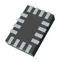
- Interface Case Style: UMLP
| Delivery and price | |
|---|---|
| Units per pack | 500 |
| Price | 0.698 € |
| Current stock | 1000+ |
| Lead time | 7 days |
## **Is Now Part of** ## **To learn more about ON Semiconductor, please visit our website at www.onsemi.com** Please note: As part of the Fairchild Semiconductor integration, some of the Fairchild orderable part numbers will need to change in order to meet ON Semiconductor’s system requirements. Since the ON Semiconductor product management systems do not have the ability to manage part nomenclature that utilizes an underscore (_), the underscore (_) in the Fairchild part numbers will be changed to a dash (-). This document may contain device numbers with an underscore (_). Please check the ON Semiconductor website to verify the updated device numbers. The most current and up-to-date ordering information can be found at www.onsemi.com. Please email any questions regarding the system integration to Fairchild_questions@onsemi.com. ON Semiconductor and the ON Semiconductor logo are trademarks of Semiconductor Components Industries, LLC dba ON Semiconductor or its subsidiaries in the United States and/or other countries. ON Semiconductor owns the rights to a number of patents, trademarks, copyrights, trade secrets, and other intellectual property. A listing of ON Semiconductor’s product/patent coverage may be accessed at www.onsemi.com/site/pdf/Patent-Marking.pdf. ON Semiconductor reserves the right to make changes without further notice to any products herein. ON Semiconductor makes no warranty, representation or guarantee regarding the suitability of its products for any particular purpose, nor does ON Semiconductor assume any liability arising out of the application or use of any product or circuit, and specifically disclaims any and all liability, including without limitation special, consequential or incidental damages. Buyer is responsible for its products and applications using ON Semiconductor products, including compliance with all laws, regulations and safety requirements or standards, regardless of any support or applications information provided by ON Semiconductor. “Typical” parameters which may be provided in ON Semiconductor data sheets and/or specifications can and do vary in different applications and actual performance may vary over time. All operating parameters, including “Typicals” must be validated for each customer application by customer’s technical experts. ON Semiconductor does not convey any license under its patent rights nor the rights of others. ON Semiconductor products are not designed, intended, or authorized for use as a critical component in life support systems or any FDA Class 3 medical devices or medical devices with a same or similar classification in a foreign jurisdiction or any devices intended for implantation in the human body. Should Buyer purchase or use ON Semiconductor products for any such unintended or unauthorized application, Buyer shall indemnify and hold ON Semiconductor and its officers, employees, subsidiaries, affiliates, and distributors harmless against all claims, costs, damages, and expenses, and reasonable attorney fees arising out of, directly or indirectly, any claim of personal injury or death associated with such unintended or unauthorized use, even if such claim alleges that ON Semiconductor was negligent regarding the design or manufacture of the part. ON Semiconductor is an Equal Opportunity/Affirmative Action Employer. This literature is subject to all applicable copyright laws and is not for resale in any manner. **==> picture [59 x 8] intentionally omitted <==** **----- Start of picture text -----**<br> October 2012<br>**----- End of picture text -----**<br> ## **FXL6408** ## **Fully Configurable 8-Bit I[2] C-Controlled GPIO Expander** ## **Features** - 4X Expansion of Connected Processor I/O Ports - Fully Integrated I[2] C Slave - 8 Independently Configurable I/O Ports - Low-Power Quiescent Current: 1.5 µA - Voltage Translation Capable from 1.65 V I[2] C Port Up to 4.0 V GPIO Pins - Selectable Device Address - 6 mA Output Drive - Interrupt Pin to Alert Processor of Status Changes ## **Description** The FXL6408 is an 8-bit I[2] C-controlled GPIO expander. When configured in Input Mode, the FXL6408 monitors the input ports for data transitions and signals the baseband by asserting the /INT pin. The input default values can be programmed independently, allowing customized input detection. All inputs can be configured with pull-up or pull-down resistors to pre-bias the inputs in open-drain or non-driven applications. When configured in Output Mode, the GPIO pins are capable of delivering 6 mA output drive according to the I[2] C register set. The FXL6408 is designed to allow voltage translation from levels as low as 1.65 V and up to 4.0 V. The FXL6408 features an active LOW RESET input as well as Power-On Reset (POR) circuit and I[2] C software reset options. **==> picture [120 x 9] intentionally omitted <==** **----- Start of picture text -----**<br> Figure 1. Block Diagram<br>**----- End of picture text -----**<br> ## **Ordering Information** |**Part Number**|**Top Mark**|**Operating**<br>**Temperature Range**|**Package**|**Packing**<br>**Method**| |---|---|---|---|---| |FXL6408UMX|XT|-40 to 85°C|16-Lead, UMLP, Quad, Ultrathin MLP,<br>1.8 X 2.6 mm Body|5000 Units on<br>Tape and Reel| www.fairchildsemi.com © 2010 Fairchild Semiconductor Corporation FXL6408 • Rev. 1.0.0 ## **Pin Configurations** |**Pin #**|**Pin Name**|**Description**| |---|---|---| |1|/INT|Interrupt output, open-drain, active LOW; requires an external pull-up resistor to VCC| |2|VDDIO|Voltage reference for I/O-side voltage translation (if I/O translation is not needed, tie<br>VDDIOto the VCCsupply)| |3|GPIO7|General-purpose programmable I/O| |4|GPIO6|General-purpose programmable I/O| |5|GPIO5|General-purpose programmable I/O| |6|GPIO4|General-purpose programmable I/O| |7|GPIO3|General-purpose programmable I/O| |8|GPIO2|General-purpose programmable I/O| |9|ADDR|Address input, GND or VCC| |10|/RST|Reset input, active LOW, requires a pull-up resistor to VCC| |11|GPIO1|General-purpose programmable I/O| |12|GPIO0|General-purpose programmable I/O| |13|SCL|I2C serial bus; requires a pull-up resistor to VCC| |14|SDA|I2C serial data; requires a pull-up resistor to VCC| |15|VCC|Supply voltage| |16|GND|Ground| ## **Pin Descriptions** © 2010 Fairchild Semiconductor Corporation FXL6408 • Rev. 1.0.0 www.fairchildsemi.com 2 ## **Absolute Maximum Ratings** Stresses exceeding the absolute maximum ratings may damage the device. The device may not function or be operable above the recommended operating conditions and stressing the parts to these levels is not recommended. In addition, extended exposure to stresses above the recommended operating conditions may affect device reliability. The absolute maximum ratings are stress ratings only. |**Symbol**|**Parameter**|**Condition**|**Min.**|**Max.**|**Unit**| |---|---|---|---|---|---| |VCC, VDDIO|Supply Voltages||-0.5|4.6|V| |VIN|DC Input Voltage||-0.5|4.0|V| |VOUT|Output Voltage(1)||-0.5|4.0|V| |IIK|DC Input Diode Current|VIN< 0 V||-50|mA| |IOK|DC Output Diode Current|VOUT< 0 V||-50|mA| |IOL|DC Output Sink Current|||+50|mA| |ICC|DC VCCor Ground Current per Supply Pin|||100|mA| |TSTG|Storage Temperature Range||-65|+150|C| |TJ|Junction Temperature under Bias|||+150|C| |TL|Junction Lead Temperature, Soldering 10 Seconds|||+260|C| |ΘJA|Thermal Resistance, Junction-to-Ambient|||115|°C/W| |ESD|Electrostatic Discharge<br>Capability|Human Body Model, JESD22-A114||4|kV| |||Charged Device Model, JESD22-C101||2|| ## **Note:** 1. All output current absolute maximum ratings must be observed. ## **Recommended Operating Conditions** The Recommended Operating Conditions table defines the conditions for actual device operation. Recommended operating conditions are specified to ensure optimal performance to the datasheet specifications. Fairchild does not recommend exceeding them or designing to Absolute Maximum Ratings. |**Symbol**|**Parameter**|**Condition**|**Min.**|**Max.**|**Unit**| |---|---|---|---|---|---| |VCC|Supply Voltage Operating||1.65|3.60|V| |VDDIO|I/O Side Reference Voltage||1.65|4.00|V| |VIN|Input Voltage on I/O pins||0|4.0|V| |VOUT|Output Voltage||0|VDDIO|V| |TA|Operating Temperature||-40|+85|°C| |tr, tf|Input Rise and Fall Times to I/O Pins<br>when Configured as Inputs|VDDIOat 1.8 V, 2.5 V ±0.2 V|0|200|ns/V| |||VDDIOat 3.6 V ± 0.3 V|0|100|| © 2010 Fairchild Semiconductor Corporation FXL6408 • Rev. 1.0.0 www.fairchildsemi.com 3 |**Symbol**|**Parameter**|**Condition**|**VCC(V)**|**TA=25°C**|**TA=25°C**|**TA=25°C**|**TA=-40 to**<br>**85°C**|**TA=-40 to**<br>**85°C**|**Unit**| |---|---|---|---|---|---|---|---|---|---| |||||**Min.**|**Typ.**|**Max. Min.**|**Max. Min.**|**Max.**|| |**RST, ADDR, SDA, SCL, /INT Pins**|||||||||| |VPOR|Power-On Reset Voltage|VDDIO=0 to 4.0 V||||1.25||1.25|V| |IIN|Input Leakage Current|0VINVCC|0 to 3.6|||±1||±10|µA| |IOFF|Power-Off Leakage<br>Current|VINor VOUT=3.6 V|0|||1||10|µA| |ICC|Standby Mode<br>(SCL in Static Condition)|VIN=VCCor GND|1.8 to 3.6|||1.2||1.5|µA| ||Active Mode(2)(SCL<br>Active)|||||300||300|| |**GPIO Pins**|||**VDDIO (V)**||||||| |VIH|HIGH Level Input Voltage||1.65 to 1.95|0.65<br>VDDIO|||0.65<br>VDDIO||V| ||||2.30 to 4.00|0.70<br>VDDIO|||0.70<br>VDDIO||| |VIL|LOW Level Input Voltage||1.65 to 1.95|-0.3||0.35<br>VDDIO|-0.3|0.35<br>VDDIO|V| ||||2.30 to 4.0|-0.3||0.30<br>VDDIO|-0.3|0.30<br>VDDIO|| |VOH|HIGH Level Output<br>Voltage|VIN=VIH,<br>IOH=100 µA|1.8|VDDIO<br>- 0.2|||VDDIO<br>- 0.2||V| ||||3.6|VDDIO<br>- 0.2|||VDDIO<br>- 0.2||| ||||4.0|VDDIO<br>- 0.2|||VDDIO<br>- 0.2||| |||IOH=6 mA|1.8|VDDIO<br>- 0.45|||VDDIO<br>- 0.45||| ||||3.6|VDDIO<br>- 0.45|||VDDIO<br>- 0.45||| |VOL|LOW Level Output Voltage|VIN=VIL,<br>IOL= -100 µA|1.8|||0.2||0.2|V| ||||3.6|||0.2||0.2|| ||||4.0|||0.2||0.2|| |||IOL=-6 mA|1.8|||0.45||0.45|| ||||3.6|||0.5||0.5|| |RPULL|Pull-Up or Pull-Down<br>Resistors||||100||||kΩ| |IOL|Output Low Current||1.8 to 4.0|6.0|||6.0||mA| |IOH|Output High Current||1.8 to 4.0|-6.0|||-6.0||| |IIN|Input Low Current(3)|0 ≤ VIN≤ VDDIO|1.8 to 4.0|||±50||±50|µA| |IOFF|Power-Off Leakage<br>Current|VIN=4.0 V|0|||1||10|µA| 2. Includes all internal circuitry consumption from the VCC supply. Does not include the I/O buffers, which are supplied by VDDIO and are load dependent. 3. IIL and IIH specifications only apply when the outputs are configured with pull-down or pull-up resistors, respectively. Specifications values assume VIN <= VDDIO. © 2010 Fairchild Semiconductor Corporation FXL6408 • Rev. 1.0.0 www.fairchildsemi.com 4 ## **AC Electrical Characteristics** All typical value are for VCC=1.8 V at TA = 25°C unless otherwise specified. **==> picture [460 x 231] intentionally omitted <==** **----- Start of picture text -----**<br> Fast Mode<br>Symbol Parameter<br>Min. Max. Unit<br>tw Reset Pulse Duration ( see Figure 4 ) 150 ns<br>tRST_GLITCH Input Glitch Rejection on RST Pin ( see Figure 4 ) 50 150 ns<br>Reset Time, Total Time from Rising Edge of Reset Pulse to Falling<br>tRESET Edge of /INT Pin ( see Figure 5 ) 150 ns<br>Time from Input Default State Change to /INT Pin Driven LOW ( see<br>tIV 4 µs<br>Figure 6 )<br>Reset Input It htc<br>| Ss _ Guaranteed to initiate<br>device reset<br>Figure 4. Reset Pulse Duration and Input Glitch Rejection Timing Diagram<br>**----- End of picture text -----**<br> **==> picture [257 x 179] intentionally omitted <==** **----- Start of picture text -----**<br> Figure 5. Reset Time and Reset Pulse Timing Diagram<br>Input not in default state<br>Saas aaa sas aa<br>Bit<br>Figure 6. Time to INT from Change in Input Default State<br>**----- End of picture text -----**<br> © 2010 Fairchild Semiconductor Corporation FXL6408 • Rev. 1.0.0 www.fairchildsemi.com 5 ## **DC Characteristics (I[2] C Controller SDA, SCL)** |**Symbol**|**Parameter**|**Parameter**|**Fast Mode(400 kHz)**|**Fast Mode(400 kHz)**|**Fast Mode(400 kHz)**| |---|---|---|---|---|---| ||||**Min.**|**Max.**|**Unit**| |VIL|Low-Level Input Voltage||-0.5|0.3 VCC|V| |VIH|High-Level Input Voltage||0.7 VCC||V| |VHYS|Hysteresis of Schmitt Trigger Inputs|VCC> 2 V|0.05 VCC||V| |||VCC< 2 V|0.1 VCC||| |VOL|Low-level Output Voltage at 3 mA Sink Current<br>(Open-Drain or Open-Collector)|VCC> 2 V|0|0.4|V| |||VCC< 2 V||0.2 VCC|V| |II|Input Current of Each I/O Pin, Input Voltage 0.26 V to 2.34 V||-10|10|µA| |CI|Capacitance for Each I/O Pin|||10|pF| ## **AC Electrical Characteristics (I[2] C Controller SDA, SCL)** All typical value are for VCC=1.8 V at TA=25°C unless otherwise specified. |**Symbol**|**Parameter**|**Fast Mode(400 kHz)**|**Fast Mode(400 kHz)**|**Fast Mode(400 kHz)**| |---|---|---|---|---| |||**Min.**|**Max.**|**Unit**| |fSCL|SCL Clock Frequency|0|400|kHz| |tHD;STA|Hold Time (Repeated) START Condition|0.6||µs| |tLOW|LOW Period of SCL Clock|1.3(4)||µs| |tHIGH|HIGH Period of SCL Clock|0.6||µs| |tSU;STA|Set Up Time for Repeated START Condition|0.6||µs| |tHD;DAT|Data Hold Time (_See Figure 7_)|0|0.9|µs| |tSU;DAT|Data Set Up Time (_See Figure 7_)|100(5)||ns| |tPS|Set Up Time Required by SDA Input Buffer (When Receiving Data)|0||ns| |tPH|Out Delay Required by SDA Output Buffer (When Transmitting Data)|300||ns| |tr|Rise Time of SDA and SCL Signals|20+0.1Cb<br>(6,7)|300|ns| |tf|Fall Time of SDA and SCL Signals|20+0.1Cb<br>(6,7)|300|ns| |tSU;STOP|Set Up Time for STOP Condition|0.6||µs| |tBUF|Bus Free Time between a STOP and START Conditions|1.3||µs| |tSP|Pulse Width of Spikes that Must Be Suppressed by the Input Filter|0|50|ns| 4. The FXL6408 can accept clock signals with LOW as low as 1.1 µs, provided that the received SDA signal tHD;DAT+ tr/f<=1.1 µs. The FXL6408 features a 0 ns SDA input setup time and, therefore, this parameter is not included in the above equation. 5. A Fast-Mode I[2] C-Bus[®] device can be used in a Standard-Mode I[2] C-Bus system, but the requirement tSU;DAT ≥ 250 ns must be met. This is automatically the case if the device does not stretch the LOW period of the SCL signal. If such a device does stretch the LOW period of the SCL signal. It must output the next data bit to the SDA line tr_max + tSU;DAT = 1000 + 250 = 1250 ns (according to the Standard-Mode I[2] C bus specification) before the SCL line is released. 6. Cb equals the total capacitance of one bus line in pF. If mixed with High-Speed Mode devices, faster fall times are allowed, according to the I[2] C specification. 7. The FXL6408 ensures that the SDA signal out must coincide with SCL LOW for worst-case SCL tf maximum times of 300 ns. This requirement prevents data loss by preventing SDA out transitions during the undefined region of the falling edge of SCL. Consequently, the FXL6408 fulfils the following requirement from the I[2] C specification, note 2 on page 77: “A device must internally provide a hold time of at least 300 ns for the SDA signal (referred to the VIHmin of the SCL signal) to bridge the undefined region of the falling edge of SCL.” 8. FXL6408 I[2] C slave is fully compliant the NXP (Phillips) I[2] C specification Rev. 0.3 UM10204 (2007). © 2010 Fairchild Semiconductor Corporation FXL6408 • Rev. 1.0.0 www.fairchildsemi.com 6 **Figure 7. Definition of Timing for Full-Speed Mode Devices on the I[2] C-Bus[®]** _Trademarks are the property of their respective owners._ © 2010 Fairchild Semiconductor Corporation FXL6408 • Rev. 1.0.0 www.fairchildsemi.com 7 ## **Functional Description** ## **Overview** The FXL6408 I/O expander frees up six ports of the central processor to be dedicated for more critical functions. The FXL6408 enables the addition of eight General-Purpose Input / Output (GPIO) ports to a system processor while using two I/O ports for I[2] C control (net six additional I/Os). The device can be used in multiple applications, from button monitoring to driving control pins of other ICs in the system. It also allows the system designer to add new features and functions quickly without upgrading the central processor. The FXL6408 includes eight I/O pins controlled by an integrated I[2] C slave and allows the central processor to control each I/O independently. When configured as outputs, each pin can deliver up to 6 mA drive. When configured as inputs, the default state can be independently configured. In addition, the FXL6408 has integrated pull-up and pull-down resistors that are enabled via I[2] C commands in the register map. This allows the system designer to pre-bias the inputs to a known level to allow use with un-driven input signals. ## **Interrupt Operation** The /INT pin is a LOW-asserted open-drain output and requires an external pull-up resistor. The FXL6408 signals an interrupt to the processor when an event occurs, removing the need for the processor to continuously poll the FXL6408 registers. Immediately after detecting a change at an input, the FXL6408 writes the corresponding bit in the input interrupt status register (13h) and asserts the /INT pin by pulling it LOW. The interrupt status register bit remains HIGH until the processor reads the register and clears the bit. If the input pin remains in the non-default state after the interrupt has been serviced, a new interrupt is not generated until after the input state has first returned to its default state and changed back to its non-default state. The FXL6408 also contains an Input Status register (0Fh) used to verify the current status of the given input at the time when the interrupt is serviced by the processor. These two registers allow the processor to determine the following information about any input every time the register map is read: ## **Device Reset** The FXL6408 has three reset options, all of which cause the part to reset all register settings to their default states. Immediately after device reset, the RST_INT bit in the Device ID & Ctrl register (01h) is HIGH and an interrupt signal is generated by the FXL6408. After the processor reads the register, this bit is cleared and, on future register reads, the processor can verify that the FXL6408 has not been reset if this bit remains LOW. Following are descriptions of the three reset methods. ## **Power-On Reset (POR)** On device power-up, when VCC reaches VPOR or if the VCC supply voltage drops below VPOR during operation, the FXL6408 immediately resets. ## **Software Reset** The FXL6408 can be reset by the processor using an I[2] C write command to change bit 0 of register 01h to a 1. Immediately following this change, the FXL6408 resets and all register values return to their default values. In this case, the SW_RST bit returns to 0 as soon as the reset sequence is completed. ## **Reset Pin** The FXL6408 is reset when the /RST pin (C3) is pulled LOW. ## **Translation** The FXL6408 has the ability to translate between the system I[2] C voltage reference and the I/O voltage reference. The VCC pin is used both as the FXL6408 power supply as well as the voltage reference for the I[2] C inputs, ADDR, /INT, and RESET pins. The VDDIO pin is used only for the voltage supply reference of the I/O ports. For example, a 1.8 V-referenced I[2] C Bus can be used to interface with the FXL6408 and control 3.6 V- referenced I/Os by supplying VCC = 1.8 V and VDDIO = 3.6 V. If translation is not needed, the system provides the same voltage to both the VCC and VDDIO pins. If both the I/O and I[2] C interfaces are referenced to 1.8 V, the VCC supply and VDDIO pin should both be tied to 1.8 V. - If the input state changed from the default state since the most recent register read; and - The current state of the input pin. The interrupt output /INT, once asserted, is held LOW until the interrupt is serviced by the processor. This means that the system uses level-sensitive interrupts. Interrupt signaling is asynchronous to the SCL signal. © 2010 Fairchild Semiconductor Corporation FXL6408 • Rev. 1.0.0 www.fairchildsemi.com 8 ## **I[2] C Read / Write Procedures** Figure 8 and Figure 9 illustrate compatible I[2] C write and read sequences. The FXL6408 does not support burst read or write optional modes described in the I[2] C standard. **==> picture [476 x 576] intentionally omitted <==** **----- Start of picture text -----**<br> 8bits 8bits 8bits<br>$+ —— -—+—,, st<br>S Slave Address WR A Register Address K A Write Data A P<br>[TO TTT<br>Figure 8. I [2] C Write Sequence<br>8bits 8bits 8bits 8bits<br>a Jt——_ -——"—__ en1<br>S Slave Address WR A Register Address K A S Slave Address RD A Read Data K NA P<br>Se<br>Single‐or multi‐byte read executed from current<br>Register address to read specified register location (single‐byte read is initiated)<br>Note: If register is not specified, the master reads from the current register.<br>Figure 9. I [2] C Read Sequence<br>From Master to Slave S Start Condition NA NOT Acknowledge (SDA High) RD Read =1<br>— From Slave to Master A Acknowledge (SDA Low) WR Write=0 P Stop Condition<br>Table 1. I [2] C Address<br>Register ADDR Pin B7 B6 B5 B4 B3 B2 B1 B0<br>ADDR=0 1 0 0 0 0 1 1 WR<br>Device Address<br>ADDR=1 1 0 0 0 1 0 0 WR<br>Table 2. I [2] C Register Map<br>Reset<br>Register Address Type B7 B6 B5 B4 B3 B2 B1 B0<br>Value<br>Device ID &<br>01h R/W MF3 MF2 MF1 FW_rev3 FW_rev2 FW_rev1 RST_INT SW_RST 10100010<br>Ctrl<br>ee eee<br>IO Direction 03h R/W GPIO7 GPIO6 GPIO5 GPIO4 GPIO3 GPIO2 GPIO1 GPIO0 00000000<br>PoE<br>Output State 05h R/W Out 7 Out 6 Out 5 Out 4 Out 3 Out 2 Out 1 Out 0 00000000<br>PoE<br>Output High-Z 07h R/W Out 7 Out 6 Out 5 Out 4 Out 3 Out 2 Out 1 Out 0 11111111<br>Po<br>Input Default 09h R/W In 7 In 6 In 5 In 4 In 3 In 2 In 1 In 0 00000000<br>State<br>ee eee<br>Pull Enable 0Bh R/W In 7 In 6 In 5 In 4 In 3 In 2 In 1 In 0 11111111<br>PoE<br>Pull-Down/<br>0Dh R/W In 7 In 6 In 5 In 4 In 3 In 2 In 1 In 0 00000000<br>eee Pull-Up<br>Input Status 0Fh R In 7 In 6 In 5 In 4 In 3 In 2 In 1 In 0 XXXXXXXX<br>Po ee<br>Interrupt Mask 11h R/W In 7 In 6 In 5 In 4 In 3 In 2 In 1 In 0 00000000<br>Po<br>Interrupt<br>13h R/W In 7 In 6 In 5 In 4 In 3 In 2 In 1 In 0 XXXXXXXX<br>Status<br>02h, 04h,<br>06h, 08h,<br>Reserved 0Ah, 0Ch, Reserved XXXXXXXX<br>OEh,10h,<br>12h<br>**----- End of picture text -----**<br> © 2010 Fairchild Semiconductor Corporation FXL6408 • Rev. 1.0.0 www.fairchildsemi.com 9 **Table 3. Device ID & Control** Address 01h RST INT flag is cleared after being read by master. For SW reset, the master writes bit 0 HIGH. **Bit# Name Bit Size Description** 3-bit manufacturer ID assigned by Nokia, Bits 7:5 are 7:5 MF 3 101 for Fairchild. 3-bit ascending value, indicating the firmware revision. 4:2 FW_rev 3 Initial revision is 000. Indicates that the device has been reset and the default values are set. 1 RST_INT 1 0: normal operation 1: the device has been reset and register default values are set. Software reset: 0 SW_RST 1 0: normal operation 1: SW reset commanded ~~=~~ **Table 4. IO Direction** Address 03h **Bit# Name Bit Size Description** 7 GPIO7 1 6 GPIO6 1 5 GPIO5 1 4 GPIO4 1 0: GPIO configured as input. 3 GPIO3 1 1: GPIO configured as output. 2 GPIO2 1 1 GPIO1 1 0 GPIO0 1 ~~=a~~ **Table 5. Output State** Address 05h If the pin is defined as input in register 03h, the corresponding bit has no effect. **Bit# Name Bit Size Description** 7 Out 7 1 6 Out 6 1 5 Out 5 1 4 Out 4 1 0: GPIO output = LOW. 3 Out 3 1 1: GPIO output = HIGH. 2 Out 2 1 1 Out 1 1 0 Out 0 1 ~~=—~~ © 2010 Fairchild Semiconductor Corporation FXL6408 • Rev. 1.0.0 10 www.fairchildsemi.com **Table 6. Output High-Z** Address 07h If the pin is defined as input in register 03h, the corresponding bit has no effect. **Bit# Name Bit Size Description** 7 Out 7 1 6 Out 6 1 5 Out 5 1 4 Out 4 1 0: GPIO output state follows register 05h 3 Out 3 1 1: GPIO output = High-Z 2 Out 2 1 1 Out 1 1 0 Out 0 1 ~~=~~ **Table 7. Input Default State** Address 09h Defines the expected state of the GPIO If the pin is defined as output in register 03h, the corresponding bit has no effect. **Bit# Name Bit Size Description** 7 In 7 1 6 In 6 1 5 In 5 1 0: GPIO input default is set to LOW; when the GPIO 4 In 4 1 goes HIGH, an interrupt is triggered. 3 In 3 1 1: GPIO input default is set to HIGH; when the GPIO goes LOW, an interrupt is triggered. 2 In 2 1 1 In 1 1 0 In 0 1 ~~=~~ **Table 8. Pull Enable** Address 0Bh - Pull enable for input pin **==> picture [489 x 222] intentionally omitted <==** **----- Start of picture text -----**<br> If the pin is defined as output in register 03h, the corresponding bit has no effect.<br>Bit# Name Bit Size Description<br>7 In 7 1<br>6 In 6 1<br>5 In 5 1<br>4 In 4 1 0: GPIO input pull-up/pull-down is not enabled.<br>3 In 3 1 1: GPIO input Pull-up/Pull-down is enabled.<br>2 In 2 1<br>1 In 1 1<br>0 In 0 1<br>=<br>© 2010 Fairchild Semiconductor Corporation<br>FXL6408 • Rev. 1.0.0 11<br>**----- End of picture text -----**<br> www.fairchildsemi.com **==> picture [508 x 383] intentionally omitted <==** **----- Start of picture text -----**<br> Table 9. Pull-Down / Pull-Up<br> Address 0Dh<br> If the pin is defined as output in register 03h, the corresponding bit has no effect.<br> If the corresponding bit in register 0Bh=0, this register setting has no effect.<br>Bit# Name Bit Size Description<br>7 In 7 1<br>6 In 6 1<br>5 In 5 1<br>4 In 4 1 0: GPIO input pull-down is enabled.<br>3 In 3 1 1: GPIO input pull-up is enabled.<br>2 In 2 1<br>1 In 1 1<br>0 In 0 1<br>=<br>Table 10. Input Status<br> Address 0Fh<br> If the pin is defined as output in register 03h, the corresponding bit has no effect.<br> This bit shows the real-time input pin status.<br>Bit# Name Bit Size Description<br>7 In 7 1<br>6 In 6 1<br>5 In 5 1<br>4 In 4 1 0: GPIO input is LOW.<br>3 In 3 1 1: GPIO input is HIGH.<br>FXL6408 — Fully Configurable 8-Bit I<br>2<br>C-Controlled GPIO Expander<br>**----- End of picture text -----**<br> **==> picture [506 x 423] intentionally omitted <==** **----- Start of picture text -----**<br> This bit shows the real-time input pin status.<br>Bit# Name Bit Size Description<br>7 In 7 1<br>6 In 6 1<br>5 In 5 1<br>4 In 4 1 0: GPIO input is LOW.<br>3 In 3 1 1: GPIO input is HIGH.<br>2 In 2 1<br>1 In 1 1<br>0 In 0 1<br>=n<br>Table 11. Interrupt Mask<br> Address 11h<br> If the pin is defined as output in register 03h, the corresponding bit has no effect.<br> This bit enables the interrupt generation from input pin state change to INT.<br>Bit# Name Bit Size Description<br>7 In 7 1<br>6 In 6 1<br>5 In 5 1<br>4 In 4 1 0: GPIO input interrupt is generated.<br>3 In 3 1 1: GPIO input interrupt is masked.<br>2 In 2 1<br>1 In 1 1<br>0 In 0 1<br>eS<br>© 2010 Fairchild Semiconductor Corporation www.fairchildsemi.com<br>FXL6408 • Rev. 1.0.0 12<br>**----- End of picture text -----**<br> ## **Table 12. Interrupt Status** - Address 13h - This bit is HIGH if input GPIO ≠ default state (register 09h). - The flag is cleared after being read by the master (bit returns to 0). - The input must go back to default state and change again before this flag is raised again. |**Bit#**|**Name**|**Bit Size**|**Description**| |---|---|---|---| |7|In 7|1|0: GPIO input is in default state or the flag has been cleared.<br>1: GPIO input has changed state from default.| |6|In 6|1|| |5|In 5|1|| |4|In 4|1|| |3|In 3|1|| |2|In 2|1|| |1|In 1|1|| |0|In 0|1|| © 2010 Fairchild Semiconductor Corporation FXL6408 • Rev. 1.0.0 www.fairchildsemi.com 13 ## **Physical Dimensions** **==> picture [413 x 502] intentionally omitted <==** **----- Start of picture text -----**<br> 0.10 C — 1.80 > A B 2.10 0.563 (15X)<br>0.663 T o l<br>2X 4 roi<br>!<br>1<br>a4<br>2.60 ! 2.90<br>PIN#1 IDENT 0.40<br>1<br>!<br>0.10 C !<br>TOP VIEW<br>2X 0.225 (16X)<br>RECOMMENDED<br>0.10 C 0.55 MAX. 0.152 LAND PATTERN<br>i<br>rh '<br>0.08 C it vi TERMINAL SHAPE VARIANTS<br>0.05 SEATING C<br>0.00 PLANE 0.40<br>SIDE VIEW 0.60<br>!!<br>0.15 i i 0.15 r 0.30<br>0.10 15X 15X<br>0.45 0.25 0.10 0.25 0.50<br>0.35 PIN 1 NON-PIN 1<br>! 5<br>Supplier 1<br>i<br>9<br>0.40 ! !<br>! 0.15 1 0.30 15X0.15 | 0.3015X<br>1 0.25 0.50 0.25 0.50<br>a A PIN 1 NON-PIN 1<br>PIN#1 IDENT<br>16 13 Supplier 2<br>0.25<br>0.55 0.15<br>0.45<br>0.10 C A B<br>BOTTOM VIEW 0.05 C<br>LEAD SHAPE AT PACKAGE EDGE<br>R0.20<br>NOTES: PACKAGE<br>EDGE<br>A. PACKAGE DOES NOT FULLY CONFORM TO ? ,<br> JEDEC STANDARD. LEAD LEAD<br>B. DIMENSIONS ARE IN MILLIMETERS. OPTION 1 OPTION 2<br>C. DIMENSIONS AND TOLERANCES PER SCALE : 2X SCALE : 2X<br> ASME Y14.5M, 1994.<br>D. LAND PATTERN RECOMMENDATION IS<br> BASED ON FSC DESIGN ONLY.<br>E. DRAWING FILENAME: MKT-UMLP16Arev4.<br>F. TERMINAL SHAPE MAY VARY ACCORDING<br> TO PACKAGE SUPPLIER, SEE TERMINAL<br> SHAPE VARIANTS.<br>Figure 10. 16-lead, UMLP, QUAD, Ultra-Thin MLP, 1.8 x 2.6 mm<br>**----- End of picture text -----**<br> _Package drawings are provided as a service to customers considering Fairchild components. Drawings may change in any manner without notice. Please note the revision and/or date on the drawing and contact a Fairchild Semiconductor representative to verify or obtain the most recent revision. Package specifications do not expand the terms of Fairchild’s worldwide terms and conditions, specifically the warranty therein, which covers Fairchild products._ _Always visit Fairchild Semiconductor’s online packaging area for the most recent package drawings: http://www.fairchildsemi.com/packaging/._ © 2010 Fairchild Semiconductor Corporation FXL6408 • Rev. 1.0.0 www.fairchildsemi.com 14 © 2010 Fairchild Semiconductor Corporation FXL6408 • Rev. 1.0.0 15 www.fairchildsemi.com ON Semiconductor and are trademarks of Semiconductor Components Industries, LLC dba ON Semiconductor or its subsidiaries in the United States and/or other countries. ON Semiconductor owns the rights to a number of patents, trademarks, copyrights, trade secrets, and other intellectual property. A listing of ON Semiconductor’s product/patent coverage may be accessed at www.onsemi.com/site/pdf/Patent−Marking.pdf. ON Semiconductor reserves the right to make changes without further notice to any products herein. ON Semiconductor makes no warranty, representation or guarantee regarding the suitability of its products for any particular purpose, nor does ON Semiconductor assume any liability arising out of the application or use of any product or circuit, and specifically disclaims any and all liability, including without limitation special, consequential or incidental damages. Buyer is responsible for its products and applications using ON Semiconductor products, including compliance with all laws, regulations and safety requirements or standards, regardless of any support or applications information provided by ON Semiconductor. “Typical” parameters which may be provided in ON Semiconductor data sheets and/or specifications can and do vary in different applications and actual performance may vary over time. All operating parameters, including “Typicals” must be validated for each customer application by customer’s technical experts. ON Semiconductor does not convey any license under its patent rights nor the rights of others. ON Semiconductor products are not designed, intended, or authorized for use as a critical component in life support systems or any FDA Class 3 medical devices or medical devices with a same or similar classification in a foreign jurisdiction or any devices intended for implantation in the human body. Should Buyer purchase or use ON Semiconductor products for any such unintended or unauthorized application, Buyer shall indemnify and hold ON Semiconductor and its officers, employees, subsidiaries, affiliates, and distributors harmless against all claims, costs, damages, and expenses, and reasonable attorney fees arising out of, directly or indirectly, any claim of personal injury or death associated with such unintended or unauthorized use, even if such claim alleges that ON Semiconductor was negligent regarding the design or manufacture of the part. ON Semiconductor is an Equal Opportunity/Affirmative Action Employer. This literature is subject to all applicable copyright laws and is not for resale in any manner. ## **PUBLICATION ORDERING INFORMATION** **N. American Technical Support** : 800−282−9855 Toll Free **ON Semiconductor Website** : **www.onsemi.com** USA/Canada ## **LITERATURE FULFILLMENT** : Literature Distribution Center for ON Semiconductor **Order Literature** : http://www.onsemi.com/orderlit For additional information, please contact your local Sales Representative 19521 E. 32nd Pkwy, Aurora, Colorado 80011 USA **Europe, Middle East and Africa Technical Support: Phone** : 303−675−2175 or 800−344−3860 Toll Free USA/Canada Phone: 421 33 790 2910 **Fax** : 303−675−2176 or 800−344−3867 Toll Free USA/Canada **Japan Customer Focus Center Email** : orderlit@onsemi.com Phone: 81−3−5817−1050 © Semiconductor Components Industries, LLC www.onsemi.com **www.onsemi.com** **1**
Updated at February 9, 2023
onsemi is a premier global supplier of intelligent power and sensing technologies, driving disruptive innovations across the automotive, industrial, and cloud infrastructure markets. Recognized for their commitment to sustainability and reliable supply chains, the company accelerates advancements in vehicle electrification, industrial automation, and 5G networks by solving the industry's most complex design challenges. At the core of their portfolio is an industry-leading selection of discrete semiconductors. This extensive range features thousands of high-performance bipolar transistors, single and dual MOSFETs, and a comprehensive array of diodes, including Zener, Schottky, and fast-recovery rectifiers. Engineered for superior thermal performance and energy efficiency, these foundational components are critical for demanding power conversion, switching, and signal conditioning applications. Beyond essential discretes, onsemi provides a robust suite of advanced power management and circuit protection solutions. Their lineup includes intelligent power modules, single IGBTs, and transient voltage suppression (TVS) diodes designed to safeguard sensitive circuitry. Complimented by integrated passive filters, AC/DC LED driver ICs, and specialized sub-2.4GHz RF transceivers, onsemi equips engineers with the scalable, high-quality technologies needed to build a cleaner, smarter, and more connected world.
About Novapart
Novapart is a B2B electronic component broker specialising in stock shortages and cost reduction. We source hard-to-find parts and identify compliant alternatives across a catalogue of 410,000+ components from 500+ manufacturers.
Learn more →Stock Shortage Specialist
When a component is unavailable, discontinued or has an unacceptable lead time, we tap into our network of vetted European and Asian distributors to source what you need — without compromising on quality or traceability.
Request a quote →Compliant Alternatives
We identify pin-to-pin, electrically equivalent substitutes that meet the same certifications (RoHS, AEC-Q100, REACH) as your original specification — validated against datasheets, not just part numbers. Often at a lower cost.
BOM Analysis service →