
Image not available
Illustrative purposes only

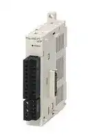
FX5-4AD-PT-ADP
EXPANSION ADAPTER, RTD I/P, PLC, 24VDC
⚠️ Reference pricing provided. In case of supply shortages, we will connect you with our trusted procurement partners to ensure your project's continuity.
- Manufacturer: MITSUBISHI
- Product type: Controller Accessories
- SVHC: No SVHC (15-Jan-2018)
- Product Range: MELSEC iQ-F FX5
- Current Rating: 20mA
| Delivery and price | |
|---|---|
| Units per pack | 1 |
| Price | 383.21 € |
| Current stock | 10+ |
| Lead time | 30 days |
Datasheet

**==> picture [57 x 63] intentionally omitted <==**
MELSEC iQ-F FX5 User's Manual (Analog Control - CPU module built-in, Expansion adapter)
## **SAFETY PRECAUTIONS**
(Read these precautions before use.)
Before using this product, please read this manual and the relevant manuals introduced in this manual carefully and pay full attention to safety in order to handle the product correctly.
This manual classifies the safety precautions into two categories: [ WARNING] and [ CAUTION].
## **WARNING**
Indicates that incorrect handling may cause hazardous conditions, resulting in death or severe injury.
## **CAUTION**
Indicates that incorrect handling may cause hazardous conditions, resulting in minor or moderate injury or property damage.
Depending on the circumstances, procedures indicated by [ CAUTION] may also cause severe injury. It is important to follow all precautions for personal safety.
Store this manual in a safe place so that it can be read whenever necessary. Always forward it to the end user.
## [DESIGN PRECAUTIONS]
## **WARNING**
- Make sure to set up the following safety circuits outside the PLC to ensure safe system operation even during external power supply problems or PLC failure. Otherwise, malfunctions may cause serious accidents.
- Most importantly, set up the following: an emergency stop circuit, a protection circuit, an interlock circuit for opposite movements (such as normal vs. reverse rotation), and an interlock circuit (to prevent damage to the equipment at the upper and lower positioning limits).
- Note that when the CPU module detects an error, such as a watchdog timer error, during selfdiagnosis, all outputs are turned off. Also, when an error that cannot be detected by the CPU module occurs in an input/output control block, output control may be disabled. External circuits and mechanisms should be designed to ensure safe machinery operation in such a case.
- Note that the output current of the 24 V DC service power supply varies depending on the model and the absence/presence of extension modules. If an overload occurs, the voltage automatically drops, inputs in the PLC are disabled, and all outputs are turned off. External circuits and mechanisms should be designed to ensure safe machinery operation in such a case.
- Note that when an error occurs in a relay, transistor or triac of an output circuit, the output might stay on or off. For output signals that may lead to serious accidents, external circuits and mechanisms should be designed to ensure safe machinery operation in such a case.
- Construct an interlock circuit in the program so that the whole system always operates on the safe side before executing the control (for data change) of the PLC in operation in such a case. Read the manual thoroughly and ensure complete safety before executing other controls (for program change, parameter change, forcible output and operation status change) of the PLC in operation. Otherwise, the machine may be damaged and accidents may occur due to erroneous operations.
- In an output circuit, when a load current exceeding the current rating or an overcurrent caused by a load short-circuit flows for a long time, it may cause smoke and fire. To prevent this, configure an external safety circuit, such as a fuse.
- For the operating status of each station after a communication failure of the network, refer to relevant manuals for the network. Incorrect output or malfunction may result in an accident.
**1**
## [DESIGN PRECAUTIONS]
## **CAUTION**
- When an inductive load such as a lamp, heater, or solenoid valve is controlled, a large current
- (approximately ten times greater than normal) may flow when the output is turned from off to on. Take proper measures so that the flowing current dose not exceed the value corresponding to the maximum load specification of the resistance load.
- After the CPU module is powered on or is reset, the time taken to enter the RUN status varies depending on the system configuration, parameter settings, and/or program size. Design circuits so that the entire system will always operate safely, regardless of this variation in time.
- ● Simultaneously turn on and off the power supplies of the CPU module and extension modules.
- If a long-time power failure or an abnormal voltage drop occurs, the PLC stops, and output is turned off. When the power supply is restored, it will automatically restart (when the RUN/STOP/RESET switch is on the RUN side).
## [INSTALLATION PRECAUTIONS]
## **WARNING**
- Make sure to cut off all phases of the power supply externally before attempting installation or wiring
- work. Failure to do so may cause electric shock or damage to the product.
- Use the product within the generic environment specifications described in the User's Manual (Hardware) of the CPU module used.
- Never use the product in areas with excessive dust, oily smoke, conductive dusts, corrosive gas (salt air, Cl2, H2S, SO2 or NO2), flammable gas, vibration or impacts, or expose it to high temperature, condensation, or rain and wind.
- If the product is used in such conditions, electric shock, fire, malfunctions, deterioration or damage may occur.
## [INSTALLATION PRECAUTIONS]
## **CAUTION**
- Do not touch the conductive parts of the product directly. Doing so may cause device failures or malfunctions.
- When drilling screw holes or wiring, make sure that cutting and wiring debris do not enter the ventilation slits of the PLC. Failure to do so may cause fire, equipment failures or malfunctions.
- For the product supplied together with a dust proof sheet, the sheet should be affixed to the ventilation slits before the installation and wiring work to prevent foreign objects such as cutting and wiring debris.
- However, when the installation work is completed, make sure to remove the sheet to provide
- adequate ventilation. Failure to do so may cause fire, equipment failures or malfunctions.
- Install the product on a flat surface. If the mounting surface is rough, undue force will be applied to the PC board, thereby causing nonconformities.
- Install the product securely using a DIN rail or mounting screws.
- Connect the expansion board and expansion adapter securely to their designated connectors. Loose connections may cause malfunctions.
- Make sure to affix the expansion board with tapping screws. Tightening torque should follow the specifications in the manual. If the screws are tightened outside of the specified torque range, poor connections may cause malfunctions.
**2**
## **CAUTION**
- Work carefully when using a screwdriver such as installation of the product. Failure to do so may cause damage to the product or accidents.
- Connect the extension cables, peripheral device cables, input/output cables and battery connecting cable securely to their designated connectors. Loose connections may cause malfunctions.
- Turn off the power to the PLC before attaching or detaching the following devices. Failure to do so may cause equipment failures or malfunctions.
- Peripheral devices, expansion board, expansion adapter, and connector conversion adapter
- Extension modules, bus conversion module, and connector conversion module
- Battery
## [WIRING PRECAUTIONS]
## **WARNING**
- Make sure to cut off all phases of the power supply externally before attempting installation or wiring work. Failure to do so may cause electric shock or damage to the product.
- Make sure to attach the terminal cover, provided as an accessory, before turning on the power or initiating operation after installation or wiring work. Failure to do so may cause electric shock.
- The temperature rating of the cable should be 80 or more.
- Make sure to wire the screw terminal block in accordance with the following precautions. Failure to do so may cause electric shock, equipment failures, a short-circuit, wire breakage, malfunctions, or damage to the product.
- The disposal size of the cable end should follow the dimensions described in the manual.
- Tightening torque should follow the specifications in the manual.
- Tighten the screws using a Phillips-head screwdriver No. 2 (shaft diameter 6 mm or less). Make sure that the screwdriver does not touch the partition part of the terminal block.
- Make sure to properly wire to the terminal block (European type) in accordance with the following precautions. Failure to do so may cause electric shock, equipment failures, a short-circuit, wire breakage, malfunctions, or damage to the product.
- The disposal size of the cable end should follow the dimensions described in the manual.
- Tightening torque should follow the specifications in the manual.
- Twist the ends of stranded wires and make sure that there are no loose wires.
- Do not solder-plate the electric wire ends.
- Do not connect more than the specified number of wires or electric wires of unspecified size.
- Affix the electric wires so that neither the terminal block nor the connected parts are directly stressed.
**3**
## [WIRING PRECAUTIONS]
## **CAUTION**
- Do not supply power to the [24+] and [24V] terminals (24 V DC service power supply) on the CPU module or extension modules. Doing so may cause damage to the product.
- Perform class D grounding (grounding resistance: 100 Ω or less) of the grounding terminal on the CPU module and extension modules with a wire 2 mm[2] or thicker.
- Do not use common grounding with heavy electrical systems (refer to the User's Manual (Hardware) of the CPU module used).
- Connect the power supply wiring to the dedicated terminals described in this manual. If an AC power supply is connected to a DC input/output terminal or DC power supply terminal, the PLC will burn out.
- Do not wire vacant terminals externally. Doing so may damage the product.
- Install module so that excessive force will not be applied to terminal blocks, power connectors, I/O connectors, communication connectors, or communication cables. Failure to do so may result in wire damage/breakage or PLC failure.
- Make sure to observe the following precautions in order to prevent any damage to the machinery or accidents due to malfunction of the PLC caused by abnormal data written to the PLC due to the effects of noise.
- Do not bundle the power line, control line and communication cables together with or lay them close to the main circuit, high-voltage line, load line or power line. As a guideline, lay the power line, control line and communication cables at least 100 mm away from the main circuit, highvoltage line, load line or power line.
- Ground the shield of the shield wire or shielded cable at one point on the PLC. However, do not use common grounding with heavy electrical systems.
- Ground the shield of the analog input/output cable at one point on the signal receiving side. However, do not use common grounding with heavy electrical systems.
## [STARTUP AND MAINTENANCE PRECAUTIONS]
## **WARNING**
- Do not touch any terminal while the PLC's power is on. Doing so may cause electric shock or malfunctions.
- Before cleaning or retightening terminals, cut off all phases of the power supply externally. Failure to do so in the power ON status may cause electric shock.
- Before modifying the program in operation, forcible output, running or stopping the PLC, read through this manual carefully, and ensure complete safety. An operation error may damage the machinery or cause accidents.
- Do not change the program in the PLC from two or more peripheral equipment devices at the same time. (i.e. from an engineering tool and a GOT) Doing so may cause destruction or malfunction of the PLC program.
**4**
## **WARNING**
- Use the battery for memory backup in conformance to the User's Manual (Hardware) of the CPU module used.
- Use the battery for the specified purpose only.
- Connect the battery correctly.
- Do not charge, disassemble, heat, put in fire, short-circuit, connect reversely, weld, swallow or burn the battery, or apply excessive forces (vibration, impact, drop, etc.) to the battery.
- Do not store or use the battery at high temperatures or expose to direct sunlight.
- Do not expose to water, bring near fire or touch liquid leakage or other contents directly.
- Incorrect handling of the battery may cause heat excessive generation, bursting, ignition, liquid leakage or deformation, and lead to injury, fire or failures and malfunction of facilities and other equipment.
## [STARTUP AND MAINTENANCE PRECAUTIONS]
## **CAUTION**
- Do not disassemble or modify the PLC. Doing so may cause fire, equipment failures, or malfunctions. For repair, contact your local Mitsubishi Electric representative.
- Turn off the power to the PLC before connecting or disconnecting any extension cable. Failure to do so may cause equipment failures or malfunctions.
- Turn off the power to the PLC before attaching or detaching the following devices. Failure to do so may cause equipment failures or malfunctions.
- Peripheral devices, expansion board, expansion adapter, and connector conversion adapter
- Extension modules, bus conversion module, and connector conversion module
- Battery
## [OPERATION PRECAUTIONS]
## **CAUTION**
- Construct an interlock circuit in the program so that the whole system always operates on the safe side before executing the control (for data change) of the PLC in operation. Read the manual thoroughly and ensure complete safety before executing other controls (for program change, parameter change, forcible output and operation status change) of the PLC in operation. Otherwise, the machine may be damaged and accidents may occur by erroneous operations.
## [DISPOSAL PRECAUTIONS]
## **CAUTION**
- Please contact a certified electronic waste disposal company for the environmentally safe recycling and disposal of your device.
- When disposing of batteries, separate them from other waste according to local regulations. (For details of the Battery Directive in EU countries, refer to the User's Manual (Hardware) of the CPU module used.)
**5**
## [TRANSPORTATION PRECAUTIONS]
## **CAUTION**
- When transporting the PLC with the optional battery, turn on the PLC before shipment, confirm that the battery mode is set using a parameter and the BAT LED is OFF, and check the battery life. If the PLC is transported with the BAT LED ON or the battery exhausted, the battery-backed data may be unstable during transportation.
- The PLC is a precision instrument. During transportation, avoid impacts larger than those specified in the general specifications of the User's Manual (Hardware) of the CPU module by using dedicated packaging boxes and shock-absorbing palettes.
- Failure to do so may cause failures in the PLC. After transportation, verify operation of the PLC and check for damage of the mounting part, etc.
- When transporting lithium batteries, follow required transportation regulations. (For details on the regulated products, refer to the User's Manual (Hardware) of the CPU module used.)
- When fumigants that contain halogen materials such as fluorine, chlorine, bromine, and iodine are used for disinfecting and protecting wooden packaging from insects, they cause malfunction when entering our products. Please take necessary precautions to ensure that remaining materials from fumigant do not enter our products, or treat packaging with methods other than fumigation (heat method). Additionally, disinfect and protect wood from insects before packing products.
**6**
## **INTRODUCTION**
This manual contains text, diagrams and explanations which will guide the reader in the correct installation, safe use and operation of the FX5 Programmable Controllers and should be read and understood before attempting to install or use the module.
Always forward it to the end user.
## **Regarding use of this product**
- This product has been manufactured as a general-purpose part for general industries, and has not been designed or manufactured to be incorporated in a device or system used in purposes related to human life.
- Before using the product for special purposes such as nuclear power, electric power, aerospace, medicine or passenger movement vehicles, consult Mitsubishi Electric.
- This product has been manufactured under strict quality control. However when installing the product where major accidents or losses could occur if the product fails, install appropriate backup or failsafe functions in the system.
## **Note**
- If in doubt at any stage during the installation of the product, always consult a professional electrical engineer who is qualified and trained in the local and national standards. If in doubt about the operation or use, please consult the nearest Mitsubishi Electric representative.
- Since the examples indicated by this manual, technical bulletin, catalog, etc. are used as a reference, please use it after confirming the function and safety of the equipment and system. Mitsubishi Electric will accept no responsibility for actual use of the product based on these illustrative examples.
- This manual content, specification etc. may be changed without a notice for improvement.
- The information in this manual has been carefully checked and is believed to be accurate; however, if you notice a doubtful point, an error, etc., please contact the nearest Mitsubishi Electric representative. When doing so, please provide the manual number given at the end of this manual.
**7**
## **CONTENTS**
|**CONTENTS**|**CONTENTS**|
|---|---|
|SAFETY PRECAUTIONS . . . . . . . . . . . . . . . . . . . . . . . . . . . . . . . . . . . . . . . . . . . . . . . . . . . . . . . . . . . . . . . . . . . .1||
|INTRODUCTION. . . . . . . . . . . . . . . . . . . . . . . . . . . . . . . . . . . . . . . . . . . . . . . . . . . . . . . . . . . . . . . . . . . . . . . . . . .7||
|RELEVANT MANUALS . . . . . . . . . . . . . . . . . . . . . . . . . . . . . . . . . . . . . . . . . . . . . . . . . . . . . . . . . . . . . . . . . . . . .18||
|TERMS . . . . . . . . . . . . . . . . . . . . . . . . . . . . . . . . . . . . . . . . . . . . . . . . . . . . . . . . . . . . . . . . . . . . . . . . . . . . . . . . .19||
|**CHAPTER 1 OUTLINE**<br>**21**||
|**CHAPTER 2 FX5-4AD-ADP**<br>**22**||
|**2.1**|**Specifications . . . . . . . . . . . . . . . . . . . . . . . . . . . . . . . . . . . . . . . . . . . . . . . . . . . . . . . . . . . . . . . . . . . . . . . . . .22**|
||Generic specifications . . . . . . . . . . . . . . . . . . . . . . . . . . . . . . . . . . . . . . . . . . . . . . . . . . . . . . . . . . . . . . . . . . . . . 22|
||Power supply specifications . . . . . . . . . . . . . . . . . . . . . . . . . . . . . . . . . . . . . . . . . . . . . . . . . . . . . . . . . . . . . . . .22|
||Performance specifications . . . . . . . . . . . . . . . . . . . . . . . . . . . . . . . . . . . . . . . . . . . . . . . . . . . . . . . . . . . . . . . . . 22|
||Input conversion characteristics . . . . . . . . . . . . . . . . . . . . . . . . . . . . . . . . . . . . . . . . . . . . . . . . . . . . . . . . . . . . .23|
||Accuracy . . . . . . . . . . . . . . . . . . . . . . . . . . . . . . . . . . . . . . . . . . . . . . . . . . . . . . . . . . . . . . . . . . . . . . . . . . . . . . . 26|
|**2.2**|**List of functions. . . . . . . . . . . . . . . . . . . . . . . . . . . . . . . . . . . . . . . . . . . . . . . . . . . . . . . . . . . . . . . . . . . . . . . . .27**|
|**2.3**|**Functions . . . . . . . . . . . . . . . . . . . . . . . . . . . . . . . . . . . . . . . . . . . . . . . . . . . . . . . . . . . . . . . . . . . . . . . . . . . . . . 28**|
||Processing of Each Function. . . . . . . . . . . . . . . . . . . . . . . . . . . . . . . . . . . . . . . . . . . . . . . . . . . . . . . . . . . . . . . . 28|
||Range Switching Function. . . . . . . . . . . . . . . . . . . . . . . . . . . . . . . . . . . . . . . . . . . . . . . . . . . . . . . . . . . . . . . . . . 29|
||A/D Conversion Enable/Disable Setting Function . . . . . . . . . . . . . . . . . . . . . . . . . . . . . . . . . . . . . . . . . . . . . . . . 30|
||A/D Conversion Method . . . . . . . . . . . . . . . . . . . . . . . . . . . . . . . . . . . . . . . . . . . . . . . . . . . . . . . . . . . . . . . . . . . 30|
||Over Scale Detection Function . . . . . . . . . . . . . . . . . . . . . . . . . . . . . . . . . . . . . . . . . . . . . . . . . . . . . . . . . . . . . . 32|
||Scaling Function . . . . . . . . . . . . . . . . . . . . . . . . . . . . . . . . . . . . . . . . . . . . . . . . . . . . . . . . . . . . . . . . . . . . . . . . .34|
||Shift Function. . . . . . . . . . . . . . . . . . . . . . . . . . . . . . . . . . . . . . . . . . . . . . . . . . . . . . . . . . . . . . . . . . . . . . . . . . . .37|
||Digital Clipping Function . . . . . . . . . . . . . . . . . . . . . . . . . . . . . . . . . . . . . . . . . . . . . . . . . . . . . . . . . . . . . . . . . . . 38|
||Maximum Value/Minimum Value Hold Function . . . . . . . . . . . . . . . . . . . . . . . . . . . . . . . . . . . . . . . . . . . . . . . . . 39|
||Warning Output Function. . . . . . . . . . . . . . . . . . . . . . . . . . . . . . . . . . . . . . . . . . . . . . . . . . . . . . . . . . . . . . . . . . . 40|
||Disconnection Detection Function. . . . . . . . . . . . . . . . . . . . . . . . . . . . . . . . . . . . . . . . . . . . . . . . . . . . . . . . . . . . 45|
||Convergence Detection Function . . . . . . . . . . . . . . . . . . . . . . . . . . . . . . . . . . . . . . . . . . . . . . . . . . . . . . . . . . . .47|
||Deviation Detection Between Channel Function . . . . . . . . . . . . . . . . . . . . . . . . . . . . . . . . . . . . . . . . . . . . . . . . . 48|
||Event History Function . . . . . . . . . . . . . . . . . . . . . . . . . . . . . . . . . . . . . . . . . . . . . . . . . . . . . . . . . . . . . . . . . . . . 49|
||Offset/gain Setting Function . . . . . . . . . . . . . . . . . . . . . . . . . . . . . . . . . . . . . . . . . . . . . . . . . . . . . . . . . . . . . . . .50|
||Offset/gain Initialization Function. . . . . . . . . . . . . . . . . . . . . . . . . . . . . . . . . . . . . . . . . . . . . . . . . . . . . . . . . . . . . 53|
||Common Function . . . . . . . . . . . . . . . . . . . . . . . . . . . . . . . . . . . . . . . . . . . . . . . . . . . . . . . . . . . . . . . . . . . . . . . .54|
|**2.4**|**Procedure to Execute the FX5-4AD-ADP . . . . . . . . . . . . . . . . . . . . . . . . . . . . . . . . . . . . . . . . . . . . . . . . . . . .55**|
|**2.5**|**Wiring . . . . . . . . . . . . . . . . . . . . . . . . . . . . . . . . . . . . . . . . . . . . . . . . . . . . . . . . . . . . . . . . . . . . . . . . . . . . . . . . .55**|
||European-type terminal block . . . . . . . . . . . . . . . . . . . . . . . . . . . . . . . . . . . . . . . . . . . . . . . . . . . . . . . . . . . . . . . 55|
||Terminal layout . . . . . . . . . . . . . . . . . . . . . . . . . . . . . . . . . . . . . . . . . . . . . . . . . . . . . . . . . . . . . . . . . . . . . . . . . .57|
||Analog input wiring . . . . . . . . . . . . . . . . . . . . . . . . . . . . . . . . . . . . . . . . . . . . . . . . . . . . . . . . . . . . . . . . . . . . . . . 57|
||Grounding . . . . . . . . . . . . . . . . . . . . . . . . . . . . . . . . . . . . . . . . . . . . . . . . . . . . . . . . . . . . . . . . . . . . . . . . . . . . . .57|
|**2.6**|**Parameter Setting . . . . . . . . . . . . . . . . . . . . . . . . . . . . . . . . . . . . . . . . . . . . . . . . . . . . . . . . . . . . . . . . . . . . . . . 58**|
||Basic settings . . . . . . . . . . . . . . . . . . . . . . . . . . . . . . . . . . . . . . . . . . . . . . . . . . . . . . . . . . . . . . . . . . . . . . . . . . . 58|
||Application settings . . . . . . . . . . . . . . . . . . . . . . . . . . . . . . . . . . . . . . . . . . . . . . . . . . . . . . . . . . . . . . . . . . . . . . . 59|
|**2.7**|**Troubleshooting . . . . . . . . . . . . . . . . . . . . . . . . . . . . . . . . . . . . . . . . . . . . . . . . . . . . . . . . . . . . . . . . . . . . . . . . 61**|
||Troubleshooting with the LEDs . . . . . . . . . . . . . . . . . . . . . . . . . . . . . . . . . . . . . . . . . . . . . . . . . . . . . . . . . . . . . . 61|
||Checking the state of the module . . . . . . . . . . . . . . . . . . . . . . . . . . . . . . . . . . . . . . . . . . . . . . . . . . . . . . . . . . . .61|
||Troubleshooting by Symptom . . . . . . . . . . . . . . . . . . . . . . . . . . . . . . . . . . . . . . . . . . . . . . . . . . . . . . . . . . . . . . . 62|
|**2.8**|**List of Error Code . . . . . . . . . . . . . . . . . . . . . . . . . . . . . . . . . . . . . . . . . . . . . . . . . . . . . . . . . . . . . . . . . . . . . . . 63**|
|**2.9**|**List of Alarm Code. . . . . . . . . . . . . . . . . . . . . . . . . . . . . . . . . . . . . . . . . . . . . . . . . . . . . . . . . . . . . . . . . . . . . . . 65**|
**8**
**==> picture [596 x 34] intentionally omitted <==**
|**2.10**|**List of Special Relays . . . . . . . . . . . . . . . . . . . . . . . . . . . . . . . . . . . . . . . . . . . . . . . . . . . . . . . . . . . . . . . . . . . . 66**|
|---|---|
|**2.11**|**Detail of Special Relays . . . . . . . . . . . . . . . . . . . . . . . . . . . . . . . . . . . . . . . . . . . . . . . . . . . . . . . . . . . . . . . . . .70**|
||A/D conversion completed flag . . . . . . . . . . . . . . . . . . . . . . . . . . . . . . . . . . . . . . . . . . . . . . . . . . . . . . . . . . . . . . 70|
||A/D conversion enable/disable setting . . . . . . . . . . . . . . . . . . . . . . . . . . . . . . . . . . . . . . . . . . . . . . . . . . . . . . . .70|
||Over scale upper limit detection flag . . . . . . . . . . . . . . . . . . . . . . . . . . . . . . . . . . . . . . . . . . . . . . . . . . . . . . . . . .70|
||Over scale lower limit detection flag . . . . . . . . . . . . . . . . . . . . . . . . . . . . . . . . . . . . . . . . . . . . . . . . . . . . . . . . . . 71|
||Over scale detection enable/disable setting . . . . . . . . . . . . . . . . . . . . . . . . . . . . . . . . . . . . . . . . . . . . . . . . . . . .71|
||Maximum value/minimum value reset completed flag. . . . . . . . . . . . . . . . . . . . . . . . . . . . . . . . . . . . . . . . . . . . . 71|
||Maximum value reset request . . . . . . . . . . . . . . . . . . . . . . . . . . . . . . . . . . . . . . . . . . . . . . . . . . . . . . . . . . . . . . .72|
||Minimum value reset request . . . . . . . . . . . . . . . . . . . . . . . . . . . . . . . . . . . . . . . . . . . . . . . . . . . . . . . . . . . . . . . 72<br>Scaling enable/disable setting. . . . . . . . . . . . . . . . . . . . . . . . . . . . . . . . . . . . . . . . . . . . . . . . . . . . . . . . . . . . . . .72<br>Digital clipping enable/disable setting . . . . . . . . . . . . . . . . . . . . . . . . . . . . . . . . . . . . . . . . . . . . . . . . . . . . . . . . . 73<br>Warning output flag (process alarm upper limit) . . . . . . . . . . . . . . . . . . . . . . . . . . . . . . . . . . . . . . . . . . . . . . . . . 73<br>Warning output flag (process alarm lower limit) . . . . . . . . . . . . . . . . . . . . . . . . . . . . . . . . . . . . . . . . . . . . . . . . . 73<br>Warning output setting (process alarm). . . . . . . . . . . . . . . . . . . . . . . . . . . . . . . . . . . . . . . . . . . . . . . . . . . . . . . . 74<br>Warning output flag (rate alarm upper) . . . . . . . . . . . . . . . . . . . . . . . . . . . . . . . . . . . . . . . . . . . . . . . . . . . . . . . .74|
||Warning output flag (rate alarm lower) . . . . . . . . . . . . . . . . . . . . . . . . . . . . . . . . . . . . . . . . . . . . . . . . . . . . . . . .74|
||Warning output setting (rate alarm) . . . . . . . . . . . . . . . . . . . . . . . . . . . . . . . . . . . . . . . . . . . . . . . . . . . . . . . . . . .75|
||Disconnection detection flag . . . . . . . . . . . . . . . . . . . . . . . . . . . . . . . . . . . . . . . . . . . . . . . . . . . . . . . . . . . . . . . .75|
||Disconnection detection enable/disable setting. . . . . . . . . . . . . . . . . . . . . . . . . . . . . . . . . . . . . . . . . . . . . . . . . .75|
||Disconnection recovery detection enable/disable setting . . . . . . . . . . . . . . . . . . . . . . . . . . . . . . . . . . . . . . . . . . 76|
||Convergence detection flag. . . . . . . . . . . . . . . . . . . . . . . . . . . . . . . . . . . . . . . . . . . . . . . . . . . . . . . . . . . . . . . . . 76|
||Convergence detection enable/disable setting . . . . . . . . . . . . . . . . . . . . . . . . . . . . . . . . . . . . . . . . . . . . . . . . . . 76|
||Deviation detection flag between channel. . . . . . . . . . . . . . . . . . . . . . . . . . . . . . . . . . . . . . . . . . . . . . . . . . . . . .77|
||Deviation detection trigger between channel. . . . . . . . . . . . . . . . . . . . . . . . . . . . . . . . . . . . . . . . . . . . . . . . . . . . 77|
||Offset/gain reading . . . . . . . . . . . . . . . . . . . . . . . . . . . . . . . . . . . . . . . . . . . . . . . . . . . . . . . . . . . . . . . . . . . . . . . 77|
||Offset/gain writing . . . . . . . . . . . . . . . . . . . . . . . . . . . . . . . . . . . . . . . . . . . . . . . . . . . . . . . . . . . . . . . . . . . . . . . . 78|
||Offset/gain initialization . . . . . . . . . . . . . . . . . . . . . . . . . . . . . . . . . . . . . . . . . . . . . . . . . . . . . . . . . . . . . . . . . . . . 78|
||A/D conversion alarm clear request . . . . . . . . . . . . . . . . . . . . . . . . . . . . . . . . . . . . . . . . . . . . . . . . . . . . . . . . . . 78|
||A/D conversion alarm flag . . . . . . . . . . . . . . . . . . . . . . . . . . . . . . . . . . . . . . . . . . . . . . . . . . . . . . . . . . . . . . . . . . 79|
||A/D conversion error flag. . . . . . . . . . . . . . . . . . . . . . . . . . . . . . . . . . . . . . . . . . . . . . . . . . . . . . . . . . . . . . . . . . . 79|
|**2.12**|**List of Special Registers. . . . . . . . . . . . . . . . . . . . . . . . . . . . . . . . . . . . . . . . . . . . . . . . . . . . . . . . . . . . . . . . . . 80**|
|**2.13**|**Detail of Special Registers . . . . . . . . . . . . . . . . . . . . . . . . . . . . . . . . . . . . . . . . . . . . . . . . . . . . . . . . . . . . . . . . 84**|
||Digital output value . . . . . . . . . . . . . . . . . . . . . . . . . . . . . . . . . . . . . . . . . . . . . . . . . . . . . . . . . . . . . . . . . . . . . . . 84|
||Digital operation value. . . . . . . . . . . . . . . . . . . . . . . . . . . . . . . . . . . . . . . . . . . . . . . . . . . . . . . . . . . . . . . . . . . . . 84|
||Analog input value monitor . . . . . . . . . . . . . . . . . . . . . . . . . . . . . . . . . . . . . . . . . . . . . . . . . . . . . . . . . . . . . . . . .84|
||Average processing specify. . . . . . . . . . . . . . . . . . . . . . . . . . . . . . . . . . . . . . . . . . . . . . . . . . . . . . . . . . . . . . . . . 85|
||Time Average/Count Average/Moving Average setting. . . . . . . . . . . . . . . . . . . . . . . . . . . . . . . . . . . . . . . . . . . . 85|
||Input range setting. . . . . . . . . . . . . . . . . . . . . . . . . . . . . . . . . . . . . . . . . . . . . . . . . . . . . . . . . . . . . . . . . . . . . . . .86|
||Maximum value . . . . . . . . . . . . . . . . . . . . . . . . . . . . . . . . . . . . . . . . . . . . . . . . . . . . . . . . . . . . . . . . . . . . . . . . . . 86|
||Minimum value . . . . . . . . . . . . . . . . . . . . . . . . . . . . . . . . . . . . . . . . . . . . . . . . . . . . . . . . . . . . . . . . . . . . . . . . . .86|
||Scaling upper limit value . . . . . . . . . . . . . . . . . . . . . . . . . . . . . . . . . . . . . . . . . . . . . . . . . . . . . . . . . . . . . . . . . . . 87|
||Scaling lower limit value . . . . . . . . . . . . . . . . . . . . . . . . . . . . . . . . . . . . . . . . . . . . . . . . . . . . . . . . . . . . . . . . . . . 87|
||Conversion value shift amount . . . . . . . . . . . . . . . . . . . . . . . . . . . . . . . . . . . . . . . . . . . . . . . . . . . . . . . . . . . . . . 87|
||Process alarm upper upper limit value . . . . . . . . . . . . . . . . . . . . . . . . . . . . . . . . . . . . . . . . . . . . . . . . . . . . . . . .88|
||Process alarm upper lower limit value. . . . . . . . . . . . . . . . . . . . . . . . . . . . . . . . . . . . . . . . . . . . . . . . . . . . . . . . . 88|
||Process alarm lower upper limit value. . . . . . . . . . . . . . . . . . . . . . . . . . . . . . . . . . . . . . . . . . . . . . . . . . . . . . . . . 89|
||Process alarm lower lower limit value . . . . . . . . . . . . . . . . . . . . . . . . . . . . . . . . . . . . . . . . . . . . . . . . . . . . . . . . . 89|
||Rate alarm upper limit value . . . . . . . . . . . . . . . . . . . . . . . . . . . . . . . . . . . . . . . . . . . . . . . . . . . . . . . . . . . . . . . .90|
||Rate alarm lower limit value . . . . . . . . . . . . . . . . . . . . . . . . . . . . . . . . . . . . . . . . . . . . . . . . . . . . . . . . . . . . . . . .90|
||Rate alarm warning detection period setting . . . . . . . . . . . . . . . . . . . . . . . . . . . . . . . . . . . . . . . . . . . . . . . . . . . . 91|
**9**
||Convergence detection upper limit value . . . . . . . . . . . . . . . . . . . . . . . . . . . . . . . . . . . . . . . . . . . . . . . . . . . . . . 91|
|---|---|
||Convergence detection lower limit value. . . . . . . . . . . . . . . . . . . . . . . . . . . . . . . . . . . . . . . . . . . . . . . . . . . . . . .92|
||Detection time setting for convergence detection . . . . . . . . . . . . . . . . . . . . . . . . . . . . . . . . . . . . . . . . . . . . . . . .92|
||Deviation detection CH1 . . . . . . . . . . . . . . . . . . . . . . . . . . . . . . . . . . . . . . . . . . . . . . . . . . . . . . . . . . . . . . . . . . . 93|
||Deviation detection CH2 . . . . . . . . . . . . . . . . . . . . . . . . . . . . . . . . . . . . . . . . . . . . . . . . . . . . . . . . . . . . . . . . . . . 93|
||Deviation value for deviation detection between channel . . . . . . . . . . . . . . . . . . . . . . . . . . . . . . . . . . . . . . . . . . 93|
||CH setting 1 for deviation detection between channel . . . . . . . . . . . . . . . . . . . . . . . . . . . . . . . . . . . . . . . . . . . .94|
||CH setting 2 for deviation detection between channel . . . . . . . . . . . . . . . . . . . . . . . . . . . . . . . . . . . . . . . . . . . .94|
||Offset setting value . . . . . . . . . . . . . . . . . . . . . . . . . . . . . . . . . . . . . . . . . . . . . . . . . . . . . . . . . . . . . . . . . . . . . . . 95|
||Gain setting value . . . . . . . . . . . . . . . . . . . . . . . . . . . . . . . . . . . . . . . . . . . . . . . . . . . . . . . . . . . . . . . . . . . . . . . . 95|
||Offset/gain writing enable code . . . . . . . . . . . . . . . . . . . . . . . . . . . . . . . . . . . . . . . . . . . . . . . . . . . . . . . . . . . . . .95|
||A/D conversion latest alarm code . . . . . . . . . . . . . . . . . . . . . . . . . . . . . . . . . . . . . . . . . . . . . . . . . . . . . . . . . . . .96|
||A/D conversion latest error code . . . . . . . . . . . . . . . . . . . . . . . . . . . . . . . . . . . . . . . . . . . . . . . . . . . . . . . . . . . . . 96|
|**CHAPTER 3 FX5-4AD-PT-ADP**<br>**97**||
|**3.1**|**Specifications . . . . . . . . . . . . . . . . . . . . . . . . . . . . . . . . . . . . . . . . . . . . . . . . . . . . . . . . . . . . . . . . . . . . . . . . . .97**|
||Generic specifications . . . . . . . . . . . . . . . . . . . . . . . . . . . . . . . . . . . . . . . . . . . . . . . . . . . . . . . . . . . . . . . . . . . . . 97|
||Power supply specifications . . . . . . . . . . . . . . . . . . . . . . . . . . . . . . . . . . . . . . . . . . . . . . . . . . . . . . . . . . . . . . . .97|
||Performance specifications . . . . . . . . . . . . . . . . . . . . . . . . . . . . . . . . . . . . . . . . . . . . . . . . . . . . . . . . . . . . . . . . . 97|
||Accuracy . . . . . . . . . . . . . . . . . . . . . . . . . . . . . . . . . . . . . . . . . . . . . . . . . . . . . . . . . . . . . . . . . . . . . . . . . . . . . . . 98|
|**3.2**|**List of functions. . . . . . . . . . . . . . . . . . . . . . . . . . . . . . . . . . . . . . . . . . . . . . . . . . . . . . . . . . . . . . . . . . . . . . . . .98**|
|**3.3**|**Functions . . . . . . . . . . . . . . . . . . . . . . . . . . . . . . . . . . . . . . . . . . . . . . . . . . . . . . . . . . . . . . . . . . . . . . . . . . . . . . 99**|
||Processing of Each Function. . . . . . . . . . . . . . . . . . . . . . . . . . . . . . . . . . . . . . . . . . . . . . . . . . . . . . . . . . . . . . . . 99|
||Temperature Unit Choice Function . . . . . . . . . . . . . . . . . . . . . . . . . . . . . . . . . . . . . . . . . . . . . . . . . . . . . . . . . . 100|
||Conversion Enable/Disable Setting Function . . . . . . . . . . . . . . . . . . . . . . . . . . . . . . . . . . . . . . . . . . . . . . . . . .100|
||Temperature Conversion Method . . . . . . . . . . . . . . . . . . . . . . . . . . . . . . . . . . . . . . . . . . . . . . . . . . . . . . . . . . .101|
||Temperature Resistance Choice Function. . . . . . . . . . . . . . . . . . . . . . . . . . . . . . . . . . . . . . . . . . . . . . . . . . . . .103|
||Disconnection Detection Function. . . . . . . . . . . . . . . . . . . . . . . . . . . . . . . . . . . . . . . . . . . . . . . . . . . . . . . . . . . 104|
||Alarm Output Function. . . . . . . . . . . . . . . . . . . . . . . . . . . . . . . . . . . . . . . . . . . . . . . . . . . . . . . . . . . . . . . . . . . . 106|
||Event History Function . . . . . . . . . . . . . . . . . . . . . . . . . . . . . . . . . . . . . . . . . . . . . . . . . . . . . . . . . . . . . . . . . . . 111|
||Offset/gain Setting Function . . . . . . . . . . . . . . . . . . . . . . . . . . . . . . . . . . . . . . . . . . . . . . . . . . . . . . . . . . . . . . . 112|
||Offset/gain Initialization Function. . . . . . . . . . . . . . . . . . . . . . . . . . . . . . . . . . . . . . . . . . . . . . . . . . . . . . . . . . . . 116|
||Maximum Value/Minimum Value Hold Function . . . . . . . . . . . . . . . . . . . . . . . . . . . . . . . . . . . . . . . . . . . . . . . . 117|
||Common Function . . . . . . . . . . . . . . . . . . . . . . . . . . . . . . . . . . . . . . . . . . . . . . . . . . . . . . . . . . . . . . . . . . . . . . . 117|
|**3.4**|**Procedure to Execute the FX5-4AD-PT-ADP. . . . . . . . . . . . . . . . . . . . . . . . . . . . . . . . . . . . . . . . . . . . . . . . . 118**|
|**3.5**|**Wiring . . . . . . . . . . . . . . . . . . . . . . . . . . . . . . . . . . . . . . . . . . . . . . . . . . . . . . . . . . . . . . . . . . . . . . . . . . . . . . . . 119**|
||European-type terminal block . . . . . . . . . . . . . . . . . . . . . . . . . . . . . . . . . . . . . . . . . . . . . . . . . . . . . . . . . . . . . . 119|
||Terminal layout . . . . . . . . . . . . . . . . . . . . . . . . . . . . . . . . . . . . . . . . . . . . . . . . . . . . . . . . . . . . . . . . . . . . . . . .120|
||Wiring of resistance temperature detector. . . . . . . . . . . . . . . . . . . . . . . . . . . . . . . . . . . . . . . . . . . . . . . . . . . . .121|
||Grounding . . . . . . . . . . . . . . . . . . . . . . . . . . . . . . . . . . . . . . . . . . . . . . . . . . . . . . . . . . . . . . . . . . . . . . . . . . . . .121|
|**3.6**|**Parameter Setting . . . . . . . . . . . . . . . . . . . . . . . . . . . . . . . . . . . . . . . . . . . . . . . . . . . . . . . . . . . . . . . . . . . . . . 122**|
||Basic settings . . . . . . . . . . . . . . . . . . . . . . . . . . . . . . . . . . . . . . . . . . . . . . . . . . . . . . . . . . . . . . . . . . . . . . . . . . 122|
||Application settings . . . . . . . . . . . . . . . . . . . . . . . . . . . . . . . . . . . . . . . . . . . . . . . . . . . . . . . . . . . . . . . . . . . . . . 123|
|**3.7**|**Troubleshooting . . . . . . . . . . . . . . . . . . . . . . . . . . . . . . . . . . . . . . . . . . . . . . . . . . . . . . . . . . . . . . . . . . . . . . . 124**|
||Troubleshooting with the LEDs . . . . . . . . . . . . . . . . . . . . . . . . . . . . . . . . . . . . . . . . . . . . . . . . . . . . . . . . . . . . . 124|
||Checking the state of the module . . . . . . . . . . . . . . . . . . . . . . . . . . . . . . . . . . . . . . . . . . . . . . . . . . . . . . . . . . .124|
||Troubleshooting by Symptom . . . . . . . . . . . . . . . . . . . . . . . . . . . . . . . . . . . . . . . . . . . . . . . . . . . . . . . . . . . . . . 126|
|**3.8**|**List of Error Code . . . . . . . . . . . . . . . . . . . . . . . . . . . . . . . . . . . . . . . . . . . . . . . . . . . . . . . . . . . . . . . . . . . . . . 127**|
|**3.9**|**List of Alarm Code. . . . . . . . . . . . . . . . . . . . . . . . . . . . . . . . . . . . . . . . . . . . . . . . . . . . . . . . . . . . . . . . . . . . . . 128**|
|**3.10**|**List of Special Relays . . . . . . . . . . . . . . . . . . . . . . . . . . . . . . . . . . . . . . . . . . . . . . . . . . . . . . . . . . . . . . . . . . . 129**|
**10**
**==> picture [596 x 34] intentionally omitted <==**
|**3.11**|**Detail of Special Relays . . . . . . . . . . . . . . . . . . . . . . . . . . . . . . . . . . . . . . . . . . . . . . . . . . . . . . . . . . . . . . . . .133**|
|---|---|
||Temperature unit selection . . . . . . . . . . . . . . . . . . . . . . . . . . . . . . . . . . . . . . . . . . . . . . . . . . . . . . . . . . . . . . . .133|
||Conversion completed flag . . . . . . . . . . . . . . . . . . . . . . . . . . . . . . . . . . . . . . . . . . . . . . . . . . . . . . . . . . . . . . . .133|
||Conversion enable/disable setting. . . . . . . . . . . . . . . . . . . . . . . . . . . . . . . . . . . . . . . . . . . . . . . . . . . . . . . . . . . 133|
||Maximum value/minimum value reset completed flag. . . . . . . . . . . . . . . . . . . . . . . . . . . . . . . . . . . . . . . . . . . . 134|
||Maximum value reset request . . . . . . . . . . . . . . . . . . . . . . . . . . . . . . . . . . . . . . . . . . . . . . . . . . . . . . . . . . . . . .134|
||Minimum value reset request . . . . . . . . . . . . . . . . . . . . . . . . . . . . . . . . . . . . . . . . . . . . . . . . . . . . . . . . . . . . . . 135|
||Warning output flag (process alarm upper limit) . . . . . . . . . . . . . . . . . . . . . . . . . . . . . . . . . . . . . . . . . . . . . . . . 135|
||Warning output flag (process alarm lower limit) . . . . . . . . . . . . . . . . . . . . . . . . . . . . . . . . . . . . . . . . . . . . . . . . 135|
||Warning output setting (Process alarm) . . . . . . . . . . . . . . . . . . . . . . . . . . . . . . . . . . . . . . . . . . . . . . . . . . . . . . 136<br>Warning output flag (rate alarm upper limit) . . . . . . . . . . . . . . . . . . . . . . . . . . . . . . . . . . . . . . . . . . . . . . . . . . .136<br>Warning output flag (rate alarm lower limit). . . . . . . . . . . . . . . . . . . . . . . . . . . . . . . . . . . . . . . . . . . . . . . . . . . . 136<br>Warning output setting (rate alarm) . . . . . . . . . . . . . . . . . . . . . . . . . . . . . . . . . . . . . . . . . . . . . . . . . . . . . . . . . .137<br>Disconnection detection flag . . . . . . . . . . . . . . . . . . . . . . . . . . . . . . . . . . . . . . . . . . . . . . . . . . . . . . . . . . . . . . .137<br>Disconnection detection enable/disable setting. . . . . . . . . . . . . . . . . . . . . . . . . . . . . . . . . . . . . . . . . . . . . . . . .137<br>Disconnection detection automatic clear enable/disable setting . . . . . . . . . . . . . . . . . . . . . . . . . . . . . . . . . . . .138|
||Offset/gain setting flag. . . . . . . . . . . . . . . . . . . . . . . . . . . . . . . . . . . . . . . . . . . . . . . . . . . . . . . . . . . . . . . . . . . . 138|
||Read offset/gain . . . . . . . . . . . . . . . . . . . . . . . . . . . . . . . . . . . . . . . . . . . . . . . . . . . . . . . . . . . . . . . . . . . . . . . .138|
||Write offset/gain. . . . . . . . . . . . . . . . . . . . . . . . . . . . . . . . . . . . . . . . . . . . . . . . . . . . . . . . . . . . . . . . . . . . . . . . . 139|
||Initialize offset/gain . . . . . . . . . . . . . . . . . . . . . . . . . . . . . . . . . . . . . . . . . . . . . . . . . . . . . . . . . . . . . . . . . . . . . . 139|
||Conversion alarm clear request. . . . . . . . . . . . . . . . . . . . . . . . . . . . . . . . . . . . . . . . . . . . . . . . . . . . . . . . . . . . .139|
||Conversion alarm flag . . . . . . . . . . . . . . . . . . . . . . . . . . . . . . . . . . . . . . . . . . . . . . . . . . . . . . . . . . . . . . . . . . . .140|
||Conversion error flag. . . . . . . . . . . . . . . . . . . . . . . . . . . . . . . . . . . . . . . . . . . . . . . . . . . . . . . . . . . . . . . . . . . . . 140|
|**3.12**|**List of Special Registers. . . . . . . . . . . . . . . . . . . . . . . . . . . . . . . . . . . . . . . . . . . . . . . . . . . . . . . . . . . . . . . . . 141**|
|**3.13**|**Detail of Special Registers . . . . . . . . . . . . . . . . . . . . . . . . . . . . . . . . . . . . . . . . . . . . . . . . . . . . . . . . . . . . . . . 145**|
||Measured temperature value. . . . . . . . . . . . . . . . . . . . . . . . . . . . . . . . . . . . . . . . . . . . . . . . . . . . . . . . . . . . . . . 145|
||Average processing setting . . . . . . . . . . . . . . . . . . . . . . . . . . . . . . . . . . . . . . . . . . . . . . . . . . . . . . . . . . . . . . . . 145|
||Time average/count average/moving average . . . . . . . . . . . . . . . . . . . . . . . . . . . . . . . . . . . . . . . . . . . . . . . . . 146|
||Setting RTD type . . . . . . . . . . . . . . . . . . . . . . . . . . . . . . . . . . . . . . . . . . . . . . . . . . . . . . . . . . . . . . . . . . . . . . . .146|
||Maximum value . . . . . . . . . . . . . . . . . . . . . . . . . . . . . . . . . . . . . . . . . . . . . . . . . . . . . . . . . . . . . . . . . . . . . . . . . 147|
||Minimum value . . . . . . . . . . . . . . . . . . . . . . . . . . . . . . . . . . . . . . . . . . . . . . . . . . . . . . . . . . . . . . . . . . . . . . . . .147|
||Process alarm upper upper limit value . . . . . . . . . . . . . . . . . . . . . . . . . . . . . . . . . . . . . . . . . . . . . . . . . . . . . . .147|
||Process alarm upper lower limit value. . . . . . . . . . . . . . . . . . . . . . . . . . . . . . . . . . . . . . . . . . . . . . . . . . . . . . . . 148|
||Process alarm lower upper limit value. . . . . . . . . . . . . . . . . . . . . . . . . . . . . . . . . . . . . . . . . . . . . . . . . . . . . . . . 148|
||Process alarm lower lower limit value . . . . . . . . . . . . . . . . . . . . . . . . . . . . . . . . . . . . . . . . . . . . . . . . . . . . . . . . 149|
||Rate alarm upper limit value . . . . . . . . . . . . . . . . . . . . . . . . . . . . . . . . . . . . . . . . . . . . . . . . . . . . . . . . . . . . . . .149|
||Rate alarm lower limit value . . . . . . . . . . . . . . . . . . . . . . . . . . . . . . . . . . . . . . . . . . . . . . . . . . . . . . . . . . . . . . .150|
||Rate alarm detection cycle setting. . . . . . . . . . . . . . . . . . . . . . . . . . . . . . . . . . . . . . . . . . . . . . . . . . . . . . . . . . . 150|
||Conversion setting for disconnection detection. . . . . . . . . . . . . . . . . . . . . . . . . . . . . . . . . . . . . . . . . . . . . . . . .151|
||Conversion setting value for disconnection detection . . . . . . . . . . . . . . . . . . . . . . . . . . . . . . . . . . . . . . . . . . . . 151|
||Offset temperature setting value . . . . . . . . . . . . . . . . . . . . . . . . . . . . . . . . . . . . . . . . . . . . . . . . . . . . . . . . . . . . 152|
||Gain temperature setting value . . . . . . . . . . . . . . . . . . . . . . . . . . . . . . . . . . . . . . . . . . . . . . . . . . . . . . . . . . . . .152|
||Offset/gain code . . . . . . . . . . . . . . . . . . . . . . . . . . . . . . . . . . . . . . . . . . . . . . . . . . . . . . . . . . . . . . . . . . . . . . . .153|
||Resistance offset value . . . . . . . . . . . . . . . . . . . . . . . . . . . . . . . . . . . . . . . . . . . . . . . . . . . . . . . . . . . . . . . . . . .153|
||Resistance gain value . . . . . . . . . . . . . . . . . . . . . . . . . . . . . . . . . . . . . . . . . . . . . . . . . . . . . . . . . . . . . . . . . . . . 154|
||Input offset value . . . . . . . . . . . . . . . . . . . . . . . . . . . . . . . . . . . . . . . . . . . . . . . . . . . . . . . . . . . . . . . . . . . . . . . .154|
||Input gain value . . . . . . . . . . . . . . . . . . . . . . . . . . . . . . . . . . . . . . . . . . . . . . . . . . . . . . . . . . . . . . . . . . . . . . . . . 154|
||Conversion latest alarm code . . . . . . . . . . . . . . . . . . . . . . . . . . . . . . . . . . . . . . . . . . . . . . . . . . . . . . . . . . . . . . 155|
||Conversion latest error code . . . . . . . . . . . . . . . . . . . . . . . . . . . . . . . . . . . . . . . . . . . . . . . . . . . . . . . . . . . . . . . 155|
**11**
|**CHAPTER 4 FX5-4AD-TC-ADP**<br>**156**|**CHAPTER 4 FX5-4AD-TC-ADP**<br>**156**|
|---|---|
|**4.1**|**Specifications . . . . . . . . . . . . . . . . . . . . . . . . . . . . . . . . . . . . . . . . . . . . . . . . . . . . . . . . . . . . . . . . . . . . . . . . .156**|
||Generic specifications . . . . . . . . . . . . . . . . . . . . . . . . . . . . . . . . . . . . . . . . . . . . . . . . . . . . . . . . . . . . . . . . . . . . 156|
||Power supply specifications . . . . . . . . . . . . . . . . . . . . . . . . . . . . . . . . . . . . . . . . . . . . . . . . . . . . . . . . . . . . . . .156|
||Performance specifications . . . . . . . . . . . . . . . . . . . . . . . . . . . . . . . . . . . . . . . . . . . . . . . . . . . . . . . . . . . . . . . . 157|
||Accuracy . . . . . . . . . . . . . . . . . . . . . . . . . . . . . . . . . . . . . . . . . . . . . . . . . . . . . . . . . . . . . . . . . . . . . . . . . . . . . . 157|
|**4.2**|**List of functions. . . . . . . . . . . . . . . . . . . . . . . . . . . . . . . . . . . . . . . . . . . . . . . . . . . . . . . . . . . . . . . . . . . . . . . .158**|
|**4.3**|**Functions . . . . . . . . . . . . . . . . . . . . . . . . . . . . . . . . . . . . . . . . . . . . . . . . . . . . . . . . . . . . . . . . . . . . . . . . . . . . . 159**|
||Processing of Each Function. . . . . . . . . . . . . . . . . . . . . . . . . . . . . . . . . . . . . . . . . . . . . . . . . . . . . . . . . . . . . . . 159|
||Temperature Unit Choice Function . . . . . . . . . . . . . . . . . . . . . . . . . . . . . . . . . . . . . . . . . . . . . . . . . . . . . . . . . . 160|
||Conversion Enable/Disable Setting Function . . . . . . . . . . . . . . . . . . . . . . . . . . . . . . . . . . . . . . . . . . . . . . . . . .160|
||Temperature Conversion Method . . . . . . . . . . . . . . . . . . . . . . . . . . . . . . . . . . . . . . . . . . . . . . . . . . . . . . . . . . .161|
||Thermocouple Type Choice Function . . . . . . . . . . . . . . . . . . . . . . . . . . . . . . . . . . . . . . . . . . . . . . . . . . . . . . . . 163|
||Disconnection Detection Function. . . . . . . . . . . . . . . . . . . . . . . . . . . . . . . . . . . . . . . . . . . . . . . . . . . . . . . . . . . 164|
||Alarm Output Function. . . . . . . . . . . . . . . . . . . . . . . . . . . . . . . . . . . . . . . . . . . . . . . . . . . . . . . . . . . . . . . . . . . . 166|
||Event History Function . . . . . . . . . . . . . . . . . . . . . . . . . . . . . . . . . . . . . . . . . . . . . . . . . . . . . . . . . . . . . . . . . . . 171|
||Offset/gain Setting Function . . . . . . . . . . . . . . . . . . . . . . . . . . . . . . . . . . . . . . . . . . . . . . . . . . . . . . . . . . . . . . .172|
||Offset/gain Initialization Function. . . . . . . . . . . . . . . . . . . . . . . . . . . . . . . . . . . . . . . . . . . . . . . . . . . . . . . . . . . . 176|
||Maximum Value/Minimum Value Hold Function . . . . . . . . . . . . . . . . . . . . . . . . . . . . . . . . . . . . . . . . . . . . . . . . 176|
||Common Function . . . . . . . . . . . . . . . . . . . . . . . . . . . . . . . . . . . . . . . . . . . . . . . . . . . . . . . . . . . . . . . . . . . . . . .177|
|**4.4**|**Procedure to Execute the FX5-4AD-TC-ADP . . . . . . . . . . . . . . . . . . . . . . . . . . . . . . . . . . . . . . . . . . . . . . . . 178**|
|**4.5**|**Wiring . . . . . . . . . . . . . . . . . . . . . . . . . . . . . . . . . . . . . . . . . . . . . . . . . . . . . . . . . . . . . . . . . . . . . . . . . . . . . . . .179**|
||European-type terminal block . . . . . . . . . . . . . . . . . . . . . . . . . . . . . . . . . . . . . . . . . . . . . . . . . . . . . . . . . . . . . . 179|
||Terminal layout . . . . . . . . . . . . . . . . . . . . . . . . . . . . . . . . . . . . . . . . . . . . . . . . . . . . . . . . . . . . . . . . . . . . . . . . .180|
||Selection of the thermocouple. . . . . . . . . . . . . . . . . . . . . . . . . . . . . . . . . . . . . . . . . . . . . . . . . . . . . . . . . . . . . .180|
||Wiring of thermocouple . . . . . . . . . . . . . . . . . . . . . . . . . . . . . . . . . . . . . . . . . . . . . . . . . . . . . . . . . . . . . . . . . . . 181|
||Grounding . . . . . . . . . . . . . . . . . . . . . . . . . . . . . . . . . . . . . . . . . . . . . . . . . . . . . . . . . . . . . . . . . . . . . . . . . . . . .181|
|**4.6**|**Parameter Setting . . . . . . . . . . . . . . . . . . . . . . . . . . . . . . . . . . . . . . . . . . . . . . . . . . . . . . . . . . . . . . . . . . . . . . 182**|
||Basic settings . . . . . . . . . . . . . . . . . . . . . . . . . . . . . . . . . . . . . . . . . . . . . . . . . . . . . . . . . . . . . . . . . . . . . . . . . . 182|
||Application settings . . . . . . . . . . . . . . . . . . . . . . . . . . . . . . . . . . . . . . . . . . . . . . . . . . . . . . . . . . . . . . . . . . . . . . 183|
|**4.7**|**Troubleshooting . . . . . . . . . . . . . . . . . . . . . . . . . . . . . . . . . . . . . . . . . . . . . . . . . . . . . . . . . . . . . . . . . . . . . . . 184**|
||Troubleshooting with the LEDs . . . . . . . . . . . . . . . . . . . . . . . . . . . . . . . . . . . . . . . . . . . . . . . . . . . . . . . . . . . . . 184|
||Checking the state of the module . . . . . . . . . . . . . . . . . . . . . . . . . . . . . . . . . . . . . . . . . . . . . . . . . . . . . . . . . . .184|
||Troubleshooting by Symptom . . . . . . . . . . . . . . . . . . . . . . . . . . . . . . . . . . . . . . . . . . . . . . . . . . . . . . . . . . . . . . 185|
|**4.8**|**List of Error Code . . . . . . . . . . . . . . . . . . . . . . . . . . . . . . . . . . . . . . . . . . . . . . . . . . . . . . . . . . . . . . . . . . . . . . 187**|
|**4.9**|**List of Alarm Code. . . . . . . . . . . . . . . . . . . . . . . . . . . . . . . . . . . . . . . . . . . . . . . . . . . . . . . . . . . . . . . . . . . . . . 188**|
|**4.10**|**List of Special Relays . . . . . . . . . . . . . . . . . . . . . . . . . . . . . . . . . . . . . . . . . . . . . . . . . . . . . . . . . . . . . . . . . . . 189**|
|**4.11**|**Detail of Special Relays . . . . . . . . . . . . . . . . . . . . . . . . . . . . . . . . . . . . . . . . . . . . . . . . . . . . . . . . . . . . . . . . .193**|
||Temperature unit selection . . . . . . . . . . . . . . . . . . . . . . . . . . . . . . . . . . . . . . . . . . . . . . . . . . . . . . . . . . . . . . . .193|
||Conversion completed flag . . . . . . . . . . . . . . . . . . . . . . . . . . . . . . . . . . . . . . . . . . . . . . . . . . . . . . . . . . . . . . . .193|
||Conversion enable/disable setting. . . . . . . . . . . . . . . . . . . . . . . . . . . . . . . . . . . . . . . . . . . . . . . . . . . . . . . . . . . 193|
||Maximum value/minimum value reset completed flag. . . . . . . . . . . . . . . . . . . . . . . . . . . . . . . . . . . . . . . . . . . . 194|
||Maximum value reset request . . . . . . . . . . . . . . . . . . . . . . . . . . . . . . . . . . . . . . . . . . . . . . . . . . . . . . . . . . . . . .194|
||Minimum value reset request . . . . . . . . . . . . . . . . . . . . . . . . . . . . . . . . . . . . . . . . . . . . . . . . . . . . . . . . . . . . . . 195|
||Warning output flag (process alarm upper limit) . . . . . . . . . . . . . . . . . . . . . . . . . . . . . . . . . . . . . . . . . . . . . . . . 195|
||Warning output flag (process alarm lower limit) . . . . . . . . . . . . . . . . . . . . . . . . . . . . . . . . . . . . . . . . . . . . . . . . 195|
||Warning output setting (process alarm). . . . . . . . . . . . . . . . . . . . . . . . . . . . . . . . . . . . . . . . . . . . . . . . . . . . . . . 196|
||Warning output flag (rate alarm upper limit) . . . . . . . . . . . . . . . . . . . . . . . . . . . . . . . . . . . . . . . . . . . . . . . . . . .196|
||Warning output flag (rate alarm lower limit). . . . . . . . . . . . . . . . . . . . . . . . . . . . . . . . . . . . . . . . . . . . . . . . . . . . 196|
||Warning output setting (rate alarm) . . . . . . . . . . . . . . . . . . . . . . . . . . . . . . . . . . . . . . . . . . . . . . . . . . . . . . . . . .197|
**12**
**==> picture [596 x 34] intentionally omitted <==**
||Disconnection detection flag . . . . . . . . . . . . . . . . . . . . . . . . . . . . . . . . . . . . . . . . . . . . . . . . . . . . . . . . . . . . . . .197|
|---|---|
||Disconnection detection enable/disable setting. . . . . . . . . . . . . . . . . . . . . . . . . . . . . . . . . . . . . . . . . . . . . . . . .197|
||Disconnection detection automatic clear enable/disable setting . . . . . . . . . . . . . . . . . . . . . . . . . . . . . . . . . . . .198|
||Offset/gain setting flag. . . . . . . . . . . . . . . . . . . . . . . . . . . . . . . . . . . . . . . . . . . . . . . . . . . . . . . . . . . . . . . . . . . . 198|
||Read offset/gain . . . . . . . . . . . . . . . . . . . . . . . . . . . . . . . . . . . . . . . . . . . . . . . . . . . . . . . . . . . . . . . . . . . . . . . .198|
||Write offset/gain. . . . . . . . . . . . . . . . . . . . . . . . . . . . . . . . . . . . . . . . . . . . . . . . . . . . . . . . . . . . . . . . . . . . . . . . . 199|
||Initialize offset/gain . . . . . . . . . . . . . . . . . . . . . . . . . . . . . . . . . . . . . . . . . . . . . . . . . . . . . . . . . . . . . . . . . . . . . . 199|
||Conversion alarm clear request. . . . . . . . . . . . . . . . . . . . . . . . . . . . . . . . . . . . . . . . . . . . . . . . . . . . . . . . . . . . .199|
||Conversion alarm flag . . . . . . . . . . . . . . . . . . . . . . . . . . . . . . . . . . . . . . . . . . . . . . . . . . . . . . . . . . . . . . . . . . . .200|
|**4.12**<br>**4.13**|Conversion error flag. . . . . . . . . . . . . . . . . . . . . . . . . . . . . . . . . . . . . . . . . . . . . . . . . . . . . . . . . . . . . . . . . . . . . 200<br>**List of Special Registers. . . . . . . . . . . . . . . . . . . . . . . . . . . . . . . . . . . . . . . . . . . . . . . . . . . . . . . . . . . . . . . . . 201**<br>**Detail of Special Registers . . . . . . . . . . . . . . . . . . . . . . . . . . . . . . . . . . . . . . . . . . . . . . . . . . . . . . . . . . . . . . . 205**<br>Measured temperature value. . . . . . . . . . . . . . . . . . . . . . . . . . . . . . . . . . . . . . . . . . . . . . . . . . . . . . . . . . . . . . . 205<br>Average processing setting . . . . . . . . . . . . . . . . . . . . . . . . . . . . . . . . . . . . . . . . . . . . . . . . . . . . . . . . . . . . . . . . 205<br>Time average/count average/moving average . . . . . . . . . . . . . . . . . . . . . . . . . . . . . . . . . . . . . . . . . . . . . . . . . 206<br>Setting thermocouple type. . . . . . . . . . . . . . . . . . . . . . . . . . . . . . . . . . . . . . . . . . . . . . . . . . . . . . . . . . . . . . . . . 206|
||Maximum value . . . . . . . . . . . . . . . . . . . . . . . . . . . . . . . . . . . . . . . . . . . . . . . . . . . . . . . . . . . . . . . . . . . . . . . . . 207|
||Minimum value . . . . . . . . . . . . . . . . . . . . . . . . . . . . . . . . . . . . . . . . . . . . . . . . . . . . . . . . . . . . . . . . . . . . . . . . .207|
||Process alarm upper upper limit value . . . . . . . . . . . . . . . . . . . . . . . . . . . . . . . . . . . . . . . . . . . . . . . . . . . . . . .207|
||Process alarm upper lower limit value. . . . . . . . . . . . . . . . . . . . . . . . . . . . . . . . . . . . . . . . . . . . . . . . . . . . . . . . 208|
||Process alarm lower upper limit value. . . . . . . . . . . . . . . . . . . . . . . . . . . . . . . . . . . . . . . . . . . . . . . . . . . . . . . . 208|
||Process alarm lower lower limit value . . . . . . . . . . . . . . . . . . . . . . . . . . . . . . . . . . . . . . . . . . . . . . . . . . . . . . . . 209|
||Rate alarm upper limit value . . . . . . . . . . . . . . . . . . . . . . . . . . . . . . . . . . . . . . . . . . . . . . . . . . . . . . . . . . . . . . .209|
||Rate alarm lower limit value . . . . . . . . . . . . . . . . . . . . . . . . . . . . . . . . . . . . . . . . . . . . . . . . . . . . . . . . . . . . . . .210|
||Rate alarm detection cycle setting. . . . . . . . . . . . . . . . . . . . . . . . . . . . . . . . . . . . . . . . . . . . . . . . . . . . . . . . . . . 210|
||Conversion setting for disconnection detection. . . . . . . . . . . . . . . . . . . . . . . . . . . . . . . . . . . . . . . . . . . . . . . . . 211|
||Conversion setting value for disconnection detection . . . . . . . . . . . . . . . . . . . . . . . . . . . . . . . . . . . . . . . . . . . . 212|
||Offset temperature setting value . . . . . . . . . . . . . . . . . . . . . . . . . . . . . . . . . . . . . . . . . . . . . . . . . . . . . . . . . . . . 212|
||Gain temperature setting value . . . . . . . . . . . . . . . . . . . . . . . . . . . . . . . . . . . . . . . . . . . . . . . . . . . . . . . . . . . . .213|
||Offset/gain code . . . . . . . . . . . . . . . . . . . . . . . . . . . . . . . . . . . . . . . . . . . . . . . . . . . . . . . . . . . . . . . . . . . . . . . .213|
||Thermal EMF offset value . . . . . . . . . . . . . . . . . . . . . . . . . . . . . . . . . . . . . . . . . . . . . . . . . . . . . . . . . . . . . . . . . 214|
||Thermal EMF gain value . . . . . . . . . . . . . . . . . . . . . . . . . . . . . . . . . . . . . . . . . . . . . . . . . . . . . . . . . . . . . . . . . . 214|
||Input offset value . . . . . . . . . . . . . . . . . . . . . . . . . . . . . . . . . . . . . . . . . . . . . . . . . . . . . . . . . . . . . . . . . . . . . . . .215|
||Input gain value . . . . . . . . . . . . . . . . . . . . . . . . . . . . . . . . . . . . . . . . . . . . . . . . . . . . . . . . . . . . . . . . . . . . . . . . . 215|
||Conversion latest alarm code . . . . . . . . . . . . . . . . . . . . . . . . . . . . . . . . . . . . . . . . . . . . . . . . . . . . . . . . . . . . . . 216|
||Conversion latest error code . . . . . . . . . . . . . . . . . . . . . . . . . . . . . . . . . . . . . . . . . . . . . . . . . . . . . . . . . . . . . . . 216|
|**CHAPTER 5 FX5-4DA-ADP**<br>**217**||
|**5.1**|**Specifications . . . . . . . . . . . . . . . . . . . . . . . . . . . . . . . . . . . . . . . . . . . . . . . . . . . . . . . . . . . . . . . . . . . . . . . . .217**|
||Generic specifications . . . . . . . . . . . . . . . . . . . . . . . . . . . . . . . . . . . . . . . . . . . . . . . . . . . . . . . . . . . . . . . . . . . . 217|
||Power supply specifications . . . . . . . . . . . . . . . . . . . . . . . . . . . . . . . . . . . . . . . . . . . . . . . . . . . . . . . . . . . . . . .217|
||Performance specifications . . . . . . . . . . . . . . . . . . . . . . . . . . . . . . . . . . . . . . . . . . . . . . . . . . . . . . . . . . . . . . . . 217|
||Output conversion characteristics . . . . . . . . . . . . . . . . . . . . . . . . . . . . . . . . . . . . . . . . . . . . . . . . . . . . . . . . . . . 218|
||Accuracy . . . . . . . . . . . . . . . . . . . . . . . . . . . . . . . . . . . . . . . . . . . . . . . . . . . . . . . . . . . . . . . . . . . . . . . . . . . . . . 221|
|**5.2**|**List of functions. . . . . . . . . . . . . . . . . . . . . . . . . . . . . . . . . . . . . . . . . . . . . . . . . . . . . . . . . . . . . . . . . . . . . . . .221**|
|**5.3**|**Functions . . . . . . . . . . . . . . . . . . . . . . . . . . . . . . . . . . . . . . . . . . . . . . . . . . . . . . . . . . . . . . . . . . . . . . . . . . . . . 222**|
||Processing of Each Function. . . . . . . . . . . . . . . . . . . . . . . . . . . . . . . . . . . . . . . . . . . . . . . . . . . . . . . . . . . . . . . 222|
||Range Switching Function. . . . . . . . . . . . . . . . . . . . . . . . . . . . . . . . . . . . . . . . . . . . . . . . . . . . . . . . . . . . . . . . . 223|
||D/A Conversion Enable/Disable Function . . . . . . . . . . . . . . . . . . . . . . . . . . . . . . . . . . . . . . . . . . . . . . . . . . . . .224|
||D/A Output Enable/Disable Setting Function. . . . . . . . . . . . . . . . . . . . . . . . . . . . . . . . . . . . . . . . . . . . . . . . . . . 224|
**13**
||Analog Output HOLD/CLEAR Function. . . . . . . . . . . . . . . . . . . . . . . . . . . . . . . . . . . . . . . . . . . . . . . . . . . . . . . 225|
|---|---|
||Analog Output Test when CPU Module is in STOP Status Function . . . . . . . . . . . . . . . . . . . . . . . . . . . . . . . . .226|
||Scaling Function . . . . . . . . . . . . . . . . . . . . . . . . . . . . . . . . . . . . . . . . . . . . . . . . . . . . . . . . . . . . . . . . . . . . . . . .227|
||Shift Function. . . . . . . . . . . . . . . . . . . . . . . . . . . . . . . . . . . . . . . . . . . . . . . . . . . . . . . . . . . . . . . . . . . . . . . . . . .229|
||Warning Output Function. . . . . . . . . . . . . . . . . . . . . . . . . . . . . . . . . . . . . . . . . . . . . . . . . . . . . . . . . . . . . . . . . . 230|
||External Power Supply Disconnection Detection Function . . . . . . . . . . . . . . . . . . . . . . . . . . . . . . . . . . . . . . . . 231|
||Disconnection Detection Function. . . . . . . . . . . . . . . . . . . . . . . . . . . . . . . . . . . . . . . . . . . . . . . . . . . . . . . . . . . 231|
||Event History Function . . . . . . . . . . . . . . . . . . . . . . . . . . . . . . . . . . . . . . . . . . . . . . . . . . . . . . . . . . . . . . . . . . . 233|
||Offset/gain Setting Function . . . . . . . . . . . . . . . . . . . . . . . . . . . . . . . . . . . . . . . . . . . . . . . . . . . . . . . . . . . . . . .233|
||Offset/gain Initialization Function. . . . . . . . . . . . . . . . . . . . . . . . . . . . . . . . . . . . . . . . . . . . . . . . . . . . . . . . . . . . 238|
||Common Function . . . . . . . . . . . . . . . . . . . . . . . . . . . . . . . . . . . . . . . . . . . . . . . . . . . . . . . . . . . . . . . . . . . . . . .239|
|**5.4**|**Procedure to Execute the FX5-4DA-ADP . . . . . . . . . . . . . . . . . . . . . . . . . . . . . . . . . . . . . . . . . . . . . . . . . . .240**|
|**5.5**|**Wiring . . . . . . . . . . . . . . . . . . . . . . . . . . . . . . . . . . . . . . . . . . . . . . . . . . . . . . . . . . . . . . . . . . . . . . . . . . . . . . . .240**|
||European-type terminal block . . . . . . . . . . . . . . . . . . . . . . . . . . . . . . . . . . . . . . . . . . . . . . . . . . . . . . . . . . . . . . 240|
||Terminal layout . . . . . . . . . . . . . . . . . . . . . . . . . . . . . . . . . . . . . . . . . . . . . . . . . . . . . . . . . . . . . . . . . . . . . . . . .241|
||Power supply wiring. . . . . . . . . . . . . . . . . . . . . . . . . . . . . . . . . . . . . . . . . . . . . . . . . . . . . . . . . . . . . . . . . . . . . . 242|
||Analog output wiring . . . . . . . . . . . . . . . . . . . . . . . . . . . . . . . . . . . . . . . . . . . . . . . . . . . . . . . . . . . . . . . . . . . . .243|
||Grounding . . . . . . . . . . . . . . . . . . . . . . . . . . . . . . . . . . . . . . . . . . . . . . . . . . . . . . . . . . . . . . . . . . . . . . . . . . . . .243|
|**5.6**|**Parameter Setting . . . . . . . . . . . . . . . . . . . . . . . . . . . . . . . . . . . . . . . . . . . . . . . . . . . . . . . . . . . . . . . . . . . . . . 244**|
||Basic settings . . . . . . . . . . . . . . . . . . . . . . . . . . . . . . . . . . . . . . . . . . . . . . . . . . . . . . . . . . . . . . . . . . . . . . . . . . 244|
||Application settings . . . . . . . . . . . . . . . . . . . . . . . . . . . . . . . . . . . . . . . . . . . . . . . . . . . . . . . . . . . . . . . . . . . . . . 245|
|**5.7**|**Troubleshooting . . . . . . . . . . . . . . . . . . . . . . . . . . . . . . . . . . . . . . . . . . . . . . . . . . . . . . . . . . . . . . . . . . . . . . . 246**|
||Troubleshooting with the LEDs . . . . . . . . . . . . . . . . . . . . . . . . . . . . . . . . . . . . . . . . . . . . . . . . . . . . . . . . . . . . . 246|
||Checking the state of the module . . . . . . . . . . . . . . . . . . . . . . . . . . . . . . . . . . . . . . . . . . . . . . . . . . . . . . . . . . .246|
||Troubleshooting by Symptom . . . . . . . . . . . . . . . . . . . . . . . . . . . . . . . . . . . . . . . . . . . . . . . . . . . . . . . . . . . . . . 247|
|**5.8**|**List of Error Code . . . . . . . . . . . . . . . . . . . . . . . . . . . . . . . . . . . . . . . . . . . . . . . . . . . . . . . . . . . . . . . . . . . . . . 249**|
|**5.9**|**List of Alarm Code. . . . . . . . . . . . . . . . . . . . . . . . . . . . . . . . . . . . . . . . . . . . . . . . . . . . . . . . . . . . . . . . . . . . . . 250**|
|**5.10**|**List of Special Relays . . . . . . . . . . . . . . . . . . . . . . . . . . . . . . . . . . . . . . . . . . . . . . . . . . . . . . . . . . . . . . . . . . . 251**|
|**5.11**|**Detail of Special Relays . . . . . . . . . . . . . . . . . . . . . . . . . . . . . . . . . . . . . . . . . . . . . . . . . . . . . . . . . . . . . . . . .253**|
||D/A conversion enable/disable setting . . . . . . . . . . . . . . . . . . . . . . . . . . . . . . . . . . . . . . . . . . . . . . . . . . . . . . .253|
||D/A output enable/disable setting . . . . . . . . . . . . . . . . . . . . . . . . . . . . . . . . . . . . . . . . . . . . . . . . . . . . . . . . . . .253|
||Scaling enable/disable setting. . . . . . . . . . . . . . . . . . . . . . . . . . . . . . . . . . . . . . . . . . . . . . . . . . . . . . . . . . . . . .254|
||Warning output upper limit value flag . . . . . . . . . . . . . . . . . . . . . . . . . . . . . . . . . . . . . . . . . . . . . . . . . . . . . . . . 254|
||Warning output lower limit value flag. . . . . . . . . . . . . . . . . . . . . . . . . . . . . . . . . . . . . . . . . . . . . . . . . . . . . . . . .254|
||Warning output setting. . . . . . . . . . . . . . . . . . . . . . . . . . . . . . . . . . . . . . . . . . . . . . . . . . . . . . . . . . . . . . . . . . . . 255|
||Disconnection detection flag . . . . . . . . . . . . . . . . . . . . . . . . . . . . . . . . . . . . . . . . . . . . . . . . . . . . . . . . . . . . . . .255|
||Disconnection detection enable/disable setting. . . . . . . . . . . . . . . . . . . . . . . . . . . . . . . . . . . . . . . . . . . . . . . . .255|
||Disconnection recovery detection enable/disable setting . . . . . . . . . . . . . . . . . . . . . . . . . . . . . . . . . . . . . . . . . 256|
||Offset/gain reading . . . . . . . . . . . . . . . . . . . . . . . . . . . . . . . . . . . . . . . . . . . . . . . . . . . . . . . . . . . . . . . . . . . . . . 256|
||Offset/gain writing . . . . . . . . . . . . . . . . . . . . . . . . . . . . . . . . . . . . . . . . . . . . . . . . . . . . . . . . . . . . . . . . . . . . . . . 256|
||Offset/gain initialization . . . . . . . . . . . . . . . . . . . . . . . . . . . . . . . . . . . . . . . . . . . . . . . . . . . . . . . . . . . . . . . . . . . 257|
||D/A conversion alarm clear request . . . . . . . . . . . . . . . . . . . . . . . . . . . . . . . . . . . . . . . . . . . . . . . . . . . . . . . . . 257|
||D/A conversion alarm flag . . . . . . . . . . . . . . . . . . . . . . . . . . . . . . . . . . . . . . . . . . . . . . . . . . . . . . . . . . . . . . . . . 257|
||D/A conversion error flag. . . . . . . . . . . . . . . . . . . . . . . . . . . . . . . . . . . . . . . . . . . . . . . . . . . . . . . . . . . . . . . . . . 258|
|**5.12**|**List of Special Registers. . . . . . . . . . . . . . . . . . . . . . . . . . . . . . . . . . . . . . . . . . . . . . . . . . . . . . . . . . . . . . . . . 259**|
|**5.13**|**Detail of Special Registers . . . . . . . . . . . . . . . . . . . . . . . . . . . . . . . . . . . . . . . . . . . . . . . . . . . . . . . . . . . . . . . 261**|
||Digital value. . . . . . . . . . . . . . . . . . . . . . . . . . . . . . . . . . . . . . . . . . . . . . . . . . . . . . . . . . . . . . . . . . . . . . . . . . . .261|
||Digital operation value. . . . . . . . . . . . . . . . . . . . . . . . . . . . . . . . . . . . . . . . . . . . . . . . . . . . . . . . . . . . . . . . . . . . 261|
||Analog output value monitor . . . . . . . . . . . . . . . . . . . . . . . . . . . . . . . . . . . . . . . . . . . . . . . . . . . . . . . . . . . . . . .262|
||HOLD/CLEAR function setting . . . . . . . . . . . . . . . . . . . . . . . . . . . . . . . . . . . . . . . . . . . . . . . . . . . . . . . . . . . . . 262|
||HOLD setting value . . . . . . . . . . . . . . . . . . . . . . . . . . . . . . . . . . . . . . . . . . . . . . . . . . . . . . . . . . . . . . . . . . . . . . 262|
**14**
**==> picture [596 x 34] intentionally omitted <==**
||Output range setting . . . . . . . . . . . . . . . . . . . . . . . . . . . . . . . . . . . . . . . . . . . . . . . . . . . . . . . . . . . . . . . . . . . . .263|
|---|---|
||Scaling upper limit value . . . . . . . . . . . . . . . . . . . . . . . . . . . . . . . . . . . . . . . . . . . . . . . . . . . . . . . . . . . . . . . . . . 263|
||Scaling lower limit value . . . . . . . . . . . . . . . . . . . . . . . . . . . . . . . . . . . . . . . . . . . . . . . . . . . . . . . . . . . . . . . . . . 263|
||Input value shift amount . . . . . . . . . . . . . . . . . . . . . . . . . . . . . . . . . . . . . . . . . . . . . . . . . . . . . . . . . . . . . . . . . . 264|
||Warning output upper limit value . . . . . . . . . . . . . . . . . . . . . . . . . . . . . . . . . . . . . . . . . . . . . . . . . . . . . . . . . . . . 264|
||Warning output lower limit value . . . . . . . . . . . . . . . . . . . . . . . . . . . . . . . . . . . . . . . . . . . . . . . . . . . . . . . . . . . .264|
||Offset setting value . . . . . . . . . . . . . . . . . . . . . . . . . . . . . . . . . . . . . . . . . . . . . . . . . . . . . . . . . . . . . . . . . . . . . . 265|
||Gain setting value . . . . . . . . . . . . . . . . . . . . . . . . . . . . . . . . . . . . . . . . . . . . . . . . . . . . . . . . . . . . . . . . . . . . . . . 265|
||Offset/gain writing enable code . . . . . . . . . . . . . . . . . . . . . . . . . . . . . . . . . . . . . . . . . . . . . . . . . . . . . . . . . . . . .265|
|D/A conversion latest alarm code . . . . . . . . . . . . . . . . . . . . . . . . . . . . . . . . . . . . . . . . . . . . . . . . . . . . . . . . . . .266<br>D/A conversion latest error code . . . . . . . . . . . . . . . . . . . . . . . . . . . . . . . . . . . . . . . . . . . . . . . . . . . . . . . . . . . . 266<br>**CHAPTER 6 FX5U CPU MODULE BUILT-IN ANALOG**<br>**267**<br>**6.1**<br>**Specifications . . . . . . . . . . . . . . . . . . . . . . . . . . . . . . . . . . . . . . . . . . . . . . . . . . . . . . . . . . . . . . . . . . . . . . . . .267**<br>Generic specifications . . . . . . . . . . . . . . . . . . . . . . . . . . . . . . . . . . . . . . . . . . . . . . . . . . . . . . . . . . . . . . . . . . . . 267||
||Performance specifications . . . . . . . . . . . . . . . . . . . . . . . . . . . . . . . . . . . . . . . . . . . . . . . . . . . . . . . . . . . . . . . . 267|
||Accuracy . . . . . . . . . . . . . . . . . . . . . . . . . . . . . . . . . . . . . . . . . . . . . . . . . . . . . . . . . . . . . . . . . . . . . . . . . . . . . . 268|
|**6.2**|**List of functions. . . . . . . . . . . . . . . . . . . . . . . . . . . . . . . . . . . . . . . . . . . . . . . . . . . . . . . . . . . . . . . . . . . . . . . .269**|
|**6.3**|**Functions (Analog input) . . . . . . . . . . . . . . . . . . . . . . . . . . . . . . . . . . . . . . . . . . . . . . . . . . . . . . . . . . . . . . . .269**|
||Processing of each function . . . . . . . . . . . . . . . . . . . . . . . . . . . . . . . . . . . . . . . . . . . . . . . . . . . . . . . . . . . . . . .270|
||A/D Conversion Enable/Disable Setting Function . . . . . . . . . . . . . . . . . . . . . . . . . . . . . . . . . . . . . . . . . . . . . . . 271|
||A/D Conversion Method . . . . . . . . . . . . . . . . . . . . . . . . . . . . . . . . . . . . . . . . . . . . . . . . . . . . . . . . . . . . . . . . . . 271|
||Over Scale Detection Function . . . . . . . . . . . . . . . . . . . . . . . . . . . . . . . . . . . . . . . . . . . . . . . . . . . . . . . . . . . . . 273|
||Scaling Function . . . . . . . . . . . . . . . . . . . . . . . . . . . . . . . . . . . . . . . . . . . . . . . . . . . . . . . . . . . . . . . . . . . . . . . .274|
||Shift Function. . . . . . . . . . . . . . . . . . . . . . . . . . . . . . . . . . . . . . . . . . . . . . . . . . . . . . . . . . . . . . . . . . . . . . . . . . .275|
||Digital Clipping Function . . . . . . . . . . . . . . . . . . . . . . . . . . . . . . . . . . . . . . . . . . . . . . . . . . . . . . . . . . . . . . . . . . 276|
||Maximum Value/Minimum Value Hold Function . . . . . . . . . . . . . . . . . . . . . . . . . . . . . . . . . . . . . . . . . . . . . . . . 276|
||Warning Output Function. . . . . . . . . . . . . . . . . . . . . . . . . . . . . . . . . . . . . . . . . . . . . . . . . . . . . . . . . . . . . . . . . . 277|
||Event History Function . . . . . . . . . . . . . . . . . . . . . . . . . . . . . . . . . . . . . . . . . . . . . . . . . . . . . . . . . . . . . . . . . . . 278|
|**6.4**|**Functions (Analog output) . . . . . . . . . . . . . . . . . . . . . . . . . . . . . . . . . . . . . . . . . . . . . . . . . . . . . . . . . . . . . . .279**|
||Processing of each function . . . . . . . . . . . . . . . . . . . . . . . . . . . . . . . . . . . . . . . . . . . . . . . . . . . . . . . . . . . . . . .279|
||D/A Conversion Enable/Disable Function . . . . . . . . . . . . . . . . . . . . . . . . . . . . . . . . . . . . . . . . . . . . . . . . . . . . .280|
||D/A Output Enable/Disable Setting Function. . . . . . . . . . . . . . . . . . . . . . . . . . . . . . . . . . . . . . . . . . . . . . . . . . . 280|
||Analog Output HOLD/CLEAR Function. . . . . . . . . . . . . . . . . . . . . . . . . . . . . . . . . . . . . . . . . . . . . . . . . . . . . . . 281|
||Analog Output Test when CPU Module is in STOP Status Function . . . . . . . . . . . . . . . . . . . . . . . . . . . . . . . . .282|
||Scaling Function . . . . . . . . . . . . . . . . . . . . . . . . . . . . . . . . . . . . . . . . . . . . . . . . . . . . . . . . . . . . . . . . . . . . . . . .283|
||Shift Function. . . . . . . . . . . . . . . . . . . . . . . . . . . . . . . . . . . . . . . . . . . . . . . . . . . . . . . . . . . . . . . . . . . . . . . . . . .284|
||Warning Output Function. . . . . . . . . . . . . . . . . . . . . . . . . . . . . . . . . . . . . . . . . . . . . . . . . . . . . . . . . . . . . . . . . . 284|
||Event History Function . . . . . . . . . . . . . . . . . . . . . . . . . . . . . . . . . . . . . . . . . . . . . . . . . . . . . . . . . . . . . . . . . . . 286|
|**6.5**|**Procedure to Execute the Built-in Analog Function . . . . . . . . . . . . . . . . . . . . . . . . . . . . . . . . . . . . . . . . . .286**|
|**6.6**|**Wiring . . . . . . . . . . . . . . . . . . . . . . . . . . . . . . . . . . . . . . . . . . . . . . . . . . . . . . . . . . . . . . . . . . . . . . . . . . . . . . . .286**|
||European-type terminal block . . . . . . . . . . . . . . . . . . . . . . . . . . . . . . . . . . . . . . . . . . . . . . . . . . . . . . . . . . . . . . 286|
||Terminal layout . . . . . . . . . . . . . . . . . . . . . . . . . . . . . . . . . . . . . . . . . . . . . . . . . . . . . . . . . . . . . . . . . . . . . . . . .287|
||Analog input wiring . . . . . . . . . . . . . . . . . . . . . . . . . . . . . . . . . . . . . . . . . . . . . . . . . . . . . . . . . . . . . . . . . . . . . . 288|
||Analog output wiring . . . . . . . . . . . . . . . . . . . . . . . . . . . . . . . . . . . . . . . . . . . . . . . . . . . . . . . . . . . . . . . . . . . . .288|
||Grounding . . . . . . . . . . . . . . . . . . . . . . . . . . . . . . . . . . . . . . . . . . . . . . . . . . . . . . . . . . . . . . . . . . . . . . . . . . . . .288|
|**6.7**|**Parameter Setting . . . . . . . . . . . . . . . . . . . . . . . . . . . . . . . . . . . . . . . . . . . . . . . . . . . . . . . . . . . . . . . . . . . . . . 289**|
||Basic settings (Analog input). . . . . . . . . . . . . . . . . . . . . . . . . . . . . . . . . . . . . . . . . . . . . . . . . . . . . . . . . . . . . . . 289|
||Application setting (Analog input) . . . . . . . . . . . . . . . . . . . . . . . . . . . . . . . . . . . . . . . . . . . . . . . . . . . . . . . . . . .290|
||Basic settings (Analog output). . . . . . . . . . . . . . . . . . . . . . . . . . . . . . . . . . . . . . . . . . . . . . . . . . . . . . . . . . . . . .291|
**15**
|Application setting (Analog output) . . . . . . . . . . . . . . . . . . . . . . . . . . . . . . . . . . . . . . . . . . . . . . . . . . . . . . . . . . 292|
|---|
|**6.8**<br>**List of Error Code . . . . . . . . . . . . . . . . . . . . . . . . . . . . . . . . . . . . . . . . . . . . . . . . . . . . . . . . . . . . . . . . . . . . . . 293**|
|**6.9**<br>**List of Alarm Code. . . . . . . . . . . . . . . . . . . . . . . . . . . . . . . . . . . . . . . . . . . . . . . . . . . . . . . . . . . . . . . . . . . . . . 294**|
|**6.10**<br>**List of Special Relays . . . . . . . . . . . . . . . . . . . . . . . . . . . . . . . . . . . . . . . . . . . . . . . . . . . . . . . . . . . . . . . . . . . 295**|
|Special relays for analog input. . . . . . . . . . . . . . . . . . . . . . . . . . . . . . . . . . . . . . . . . . . . . . . . . . . . . . . . . . . . . .295|
|Special relays for analog output . . . . . . . . . . . . . . . . . . . . . . . . . . . . . . . . . . . . . . . . . . . . . . . . . . . . . . . . . . . .295|
|**6.11**<br>**List of Special Registers. . . . . . . . . . . . . . . . . . . . . . . . . . . . . . . . . . . . . . . . . . . . . . . . . . . . . . . . . . . . . . . . . 296**|
|Special registers for analog input . . . . . . . . . . . . . . . . . . . . . . . . . . . . . . . . . . . . . . . . . . . . . . . . . . . . . . . . . . .296|
|Special registers for analog output . . . . . . . . . . . . . . . . . . . . . . . . . . . . . . . . . . . . . . . . . . . . . . . . . . . . . . . . . . 296|
|**6.12**<br>**How to use analog inputs built in CPU module for current inputs. . . . . . . . . . . . . . . . . . . . . . . . . . . . . . . 297**|
|**APPENDIX**<br>**298**|
|**Appendix 1 Added and Enhanced Functions . . . . . . . . . . . . . . . . . . . . . . . . . . . . . . . . . . . . . . . . . . . . . . . . . . . . . 298**|
|**INDEX**<br>**300**|
|REVISIONS. . . . . . . . . . . . . . . . . . . . . . . . . . . . . . . . . . . . . . . . . . . . . . . . . . . . . . . . . . . . . . . . . . . . . . . . . . . . .302|
|WARRANTY . . . . . . . . . . . . . . . . . . . . . . . . . . . . . . . . . . . . . . . . . . . . . . . . . . . . . . . . . . . . . . . . . . . . . . . . . . . .303|
|TRADEMARKS . . . . . . . . . . . . . . . . . . . . . . . . . . . . . . . . . . . . . . . . . . . . . . . . . . . . . . . . . . . . . . . . . . . . . . . . . .304|
**16**
**==> picture [596 x 34] intentionally omitted <==**
**17**
## **RELEVANT MANUALS**
|**Manual name <manual number>**|**Description**|
|---|---|
|MELSEC iQ-F FX5 User's Manual (Startup)<br><JY997D58201>|Performance specifications, procedures before operation, and troubleshooting of the<br>CPU module.|
|MELSEC iQ-F FX5U User's Manual (Hardware)<br><JY997D55301>|Describes the details of hardware of the FX5U CPU module, including input/output<br>specifications, wiring, installation, and maintenance.|
|MELSEC iQ-F FX5UC User's Manual (Hardware)<br><JY997D61401>|Describes the details of hardware of the FX5UC CPU module, including input/output<br>specifications, wiring, installation, and maintenance.|
|MELSEC iQ-F FX5 User's Manual (Application)<br><JY997D55401>|Describes basic knowledge required for program design, functions of the CPU<br>module, devices/labels, and parameters.|
|MELSEC iQ-F FX5 Programming Manual (Program Design)<br><JY997D55701>|Describes specifications of ladders, ST, FBD/LD, and other programs and labels.|
|MELSEC iQ-F FX5 Programming Manual (Instructions, Standard<br>Functions/Function Blocks)<br><JY997D55801>|Describes specifications of instructions and functions that can be used in programs.|
|MELSEC iQ-F FX5 User's Manual (Serial Communication)<br><JY997D55901>|Describes N:N network, Parallel link, MELSEC Communication protocol, inverter<br>communication, non-protocol communication, and predefined protocol support.|
|MELSEC iQ-F FX5 User's Manual (MELSEC Communication Protocol)<br><JY997D60801>|Explains methods for the device that is communicating with the CPU module by MC<br>protocol to read and write the data of the CPU module.|
|MELSEC iQ-F FX5 User's Manual (MODBUS Communication)<br><JY997D56101>|Describes MODBUS serial communication.|
|MELSEC iQ-F FX5 User's Manual (Ethernet Communication)<br><JY997D56201>|Describes the functions of the built-in Ethernet port communication function.|
|MELSEC iQ-F FX5 User's Manual (SLMP)<br><JY997D56001>|Explains methods for the device that is communicating with the CPU module by<br>SLMP to read and write the data of the CPU module.|
|MELSEC iQ-F FX5 User's Manual (CC-Link IE)<br><JY997D64201>|Describes CC-Link IE field network module.|
|MELSEC iQ-F FX5 User's Manual (CC-Link)<br><SH-081793ENG>|Describes CC-Link system master/intelligent device module.|
|MELSEC iQ-F FX5 User's Manual (ASLINK)<br><SH-081796ENG>|Describes AnyWireASLINK system master module.|
|MELSEC iQ-F FX5 User's Manual (Positioning Control - CPU module<br>built-in, High-speed pulse input/output module)<br><JY997D56301>|Describes the positioning function of the CPU module built-in and the high-speed<br>pulse input/output module.|
|MELSEC iQ-F FX5 User's Manual (Positioning Control - Intelligent<br>function module)<br><SH-081805ENG>|Describes the positioning module.|
|MELSEC iQ-F FX5 Simple Motion Module User's Manual (Startup)<br><IB0300251>|Specifications, procedures before operation, system configuration, wiring, and<br>operation examples of the Simple Motion module.|
|MELSEC iQ-F FX5 Simple Motion Module User's Manual (Application)<br><IB0300253>|Functions, input/output signals, buffer memories, parameter settings, programming,<br>and troubleshooting of the Simple Motion module.|
|MELSEC iQ-F FX5 Simple Motion Module User's Manual (Advanced<br>Synchronous Control)<br><IB0300255>|Functions and programming for the synchronous control of the Simple Motion<br>module.|
|MELSEC iQ-F FX5 User's Manual (Analog Control - CPU module built-<br>in, Expansion adapter)<br><JY997D60501> (This manual)|Describes the analog function of the CPU module built-in and the analog adapter.|
|MELSEC iQ-F FX5 User's Manual (Analog Control - Intelligent function<br>module)<br><SH-081802ENG>|Describes the multiple input module (voltage, current, thermocouple, and resistance<br>temperature detector).|
|MELSEC iQ-F FX5 User's Manual (Temperature Control)<br><SH-081799ENG>|Describes the temperature control module.|
|GX Works3 Operating Manual<br><SH-081215ENG>|System configuration, parameter settings, and online operations of GX Works3.|
|Transition from MELSEC FX3U, FX3UC Series to MELSEC iQ-F<br>Series Handbook<br><JY997D66201>|Describes the transition from MELSEC FX3U/FX3UC series to MELSEC iQ-F series.|
**18**
## **TERMS**
Unless otherwise specified, this manual uses the following terms.
For details on the FX3 devices that can be connected with the FX5, refer to the User’s Manual (Hardware) of the CPU module to be used.
|**Terms**|**Description**|
|---|---|
|■Devices||
|FX5|Generic term for FX5U and FX5UC PLCs|
|FX3|Generic term for FX3S, FX3G, FX3GC, FX3U, and FX3UC PLCs|
|FX5 CPU module|Generic term for FX5U CPU module and FX5UC CPU module|
|FX5U CPU module|Generic term for FX5U-32MR/ES, FX5U-32MT/ES, FX5U-32MT/ESS, FX5U-64MR/ES, FX5U-64MT/ES,<br>FX5U-64MT/ESS, FX5U-80MR/ES, FX5U-80MT/ES, FX5U-80MT/ESS, FX5U-32MR/DS, FX5U-32MT/DS,<br>FX5U-32MT/DSS, FX5U-64MR/DS, FX5U-64MT/DS, FX5U-64MT/DSS, FX5U-80MR/DS, FX5U-80MT/DS, and<br>FX5U-80MT/DSS|
|FX5UC CPU module|Generic term for FX5UC-32MT/D, FX5UC-32MT/DSS, FX5UC-64MT/D, FX5UC-64MT/DSS, FX5UC-96MT/D,<br>and FX5UC-96MT/DSS|
|Extension module|Generic term for FX5 extension modules and FX3 function modules|
|• FX5 extension module|Generic term for I/O modules, FX5 extension power supply modules, and FX5 intelligent function modules|
|• FX3 extension module|Generic term for FX3 extension power supply module and FX3 intelligent function module|
|• Extension module (extension cable type)|Generic term for Input modules (extension cable type), Output modules (extension cable type), Input/output<br>modules (extension cable type), Powered input/output module, High-speed pulse input/output module,<br>Extension power supply module (extension cable type), Connector conversion module (extension cable type),<br>Intelligent function modules, and Bus conversion module (extension cable type)|
|• Extension module (extension connector<br>type)|Generic term for Input modules (extension connector type), Output modules (extension connector type), Input/<br>output modules (extension connector type), Extension power supply module (extension connector type),<br>Connector conversion module (extension connector type), and Bus conversion module (extension connector<br>type)|
|I/O module|Generic term for Input modules, Output modules, Input/output modules, Powered input/output modules, and<br>High-speed pulse input/output modules|
|Input module|Generic term for Input modules (extension cable type) and Input modules (extension connector type)|
|• Input module (extension cable type)|Generic term for FX5-8EX/ES and FX5-16EX/ES|
|• Input module (extension connector type)|Generic term for FX5-C16EX/D, FX5-C16EX/DS, FX5-C32EX/D, and FX5-C32EX/DS|
|Output module|Generic term for Output modules (extension cable type) and Output modules (extension connector type)|
|• Output module (extension cable type)|Generic term for FX5-8EYR/ES, FX5-8EYT/ES, FX5-8EYT/ESS, FX5-16EYR/ES, FX5-16EYT/ES, and FX5-<br>16EYT/ESS|
|• Output module (extension connector type)|Generic term for FX5-C16EYT/D, FX5-C16EYT/DSS, FX5-C32EYT/D, and FX5-C32EYT/DSS|
|Input/output module|Generic term for Input/output modules (extension cable type) and Input/output modules (extension connector<br>type)|
|• Input/output module (extension cable<br>type)|Generic term for FX5-16ER/ES, FX5-16ET/ES, and FX5-16ET/ESS|
|• Input/output module (extension connector<br>type)|Generic term for FX5-C32ET/D and FX5-C32ET/DSS|
|Powered input/output module|Generic term for FX5-32ER/ES, FX5-32ET/ES, FX5-32ET/ESS, FX5-32ER/DS, FX5-32ET/DS, and FX5-32ET/<br>DSS|
|High-speed pulse input/output module|Generic term for FX5-16ET/ES-H and FX5-16ET/ESS-H|
|Extension power supply module|Generic term for FX5 extension power supply module and FX3 extension power supply module|
|• FX5 extension power supply module|Generic term for FX5 extension power supply module (extension cable type) and FX5 extension power supply<br>module (extension connector type)|
|• FX5 extension power supply module<br>(extension cable type)|Different name for FX5-1PSU-5V|
|• FX5 extension power supply module<br>(extension connector type)|Different name for FX5-C1PS-5V|
|• FX3 extension power supply module|Different name for FX3U-1PSU-5V|
|Intelligent module|The abbreviation for intelligent function modules|
|Intelligent function module|Generic term for FX5 intelligent function modules and FX3 intelligent function modules|
|• FX5 intelligent function module|Generic term for FX5-8AD, FX5-4LC, FX5-20PG-P, FX5-40SSC-S, FX5-80SSC-S, FX5-CCLIEF, FX5-CCL-MS,<br>and FX5-ASL-M|
**19**
|**Terms**|**Description**|
|---|---|
|• FX3 intelligent function module|Generic term for FX3U-4AD, FX3U-4DA, FX3U-4LC, FX3U-1PG, FX3U-2HC, FX3U-16CCL-M, FX3U-64CCL,<br>and FX3U-128ASL-M|
|Expansion board|Generic term for board for FX5U CPU module|
|• Communication board|Generic term for FX5-232-BD, FX5-485-BD, and FX5-422-BD-GOT|
|Expansion adapter|Generic term for adapter for FX5 CPU module|
|• Communication adapter|Generic term for FX5-232ADP and FX5-485ADP|
|• Analog adapter|Generic term for FX5-4AD-ADP, FX5-4DA-ADP, FX5-4AD-PT-ADP, and FX5-4AD-TC-ADP|
|Bus conversion module|Generic term for Bus conversion module (extension cable type) and Bus conversion module (extension<br>connector type)|
|• Bus conversion module (extension cable<br>type)|Different name for FX5-CNV-BUS|
|• Bus conversion module (extension<br>connector type)|Different name for FX5-CNV-BUSC|
|Connector conversion module|Generic term for Connector conversion module (extension cable type) and Connector conversion module<br>(extension connector type)|
|• Connector conversion module (extension<br>cable type)|Different name for FX5-CNV-IF|
|• Connector conversion module (extension<br>connector type)|Different name for FX5-CNV-IFC|
|Extended extension cable|Generic term for FX5-30EC and FX5-65EC|
|Connector conversion adapter|Different name for FX5-CNV-BC|
|Battery|Different name for FX3U-32BL|
|Peripheral device|Generic term for engineering tools and GOTs|
|GOT|Generic term for Mitsubishi Electric Graphic Operation Terminal GOT1000 and GOT2000 series|
|■Software packages||
|Engineering tool|The product name of the software package for the MELSEC programmable controllers|
|GX Works3|The product name of the software package, SWnDND-GXW3, for the MELSEC programmable controllers (The<br>'n' represents a version.)|
**20**
**1 OUTLINE**
**1**
The FX5 supports the following analog functions:
|**Item**|**Outline**|**Reference**|
|---|---|---|
|FX5-4AD-ADP (Analog input)|The FX5-4AD-ADP is an analog adapter which inputs 4 points of analog<br>input (voltage/current) when connected to the FX5 CPU module.<br>A/D-converted values are written to special registers assigned to each<br>channel.<br>Up to four of all analog adapter types can be connected.|Page 22|
|FX5-4AD-PT-ADP (Temperature input)|The FX5-4AD-PT-ADP is an analog adapter which inputs 4 points of<br>temperature of resistance temperature detector (analog input) when<br>connected to the FX5 CPU module.<br>Temperature converted values are written to special registers assigned to<br>each channel.<br>Up to four of all analog adapter types can be connected.|Page 97|
|FX5-4AD-TC-ADP (Temperature input)|The FX5-4AD-TC-ADP is an analog adapter which inputs 4 points of<br>temperature of thermocouple (analog input) when connected to the FX5<br>CPU module.<br>Temperature converted values are written to special registers assigned to<br>each channel.<br>Up to four of all analog adapter types can be connected.|Page 156|
|FX5-4DA-ADP (Analog output)|The FX5-4DA-ADP is an analog adapter which outputs 4 points of<br>voltage/current when connected to the FX5 CPU module.<br>D/A-converted analog data are output when values are set to special<br>registers assigned to each channel.<br>Up to four of all analog adapter types can be connected.|Page 217|
|FX5U CPU module built-in analog (Analog input/<br>output)|The FX5 CPU module has 2 points of built-in analog voltage input and 1<br>point of built-in analog voltage output.<br>Values A/D-converted by the FX5U CPU module are written to special<br>registers assigned to each channel.<br>D/A-converted analog data are output when values are set to special<br>registers in the FX5U CPU module.|Page 267|
1 OUTLINE
**21**
**2 FX5-4AD-ADP**
This chapter describes the FX5-4AD-ADP.
## **2.1 Specifications**
This section describes the specifications.
## **Generic specifications**
The items other than the following are equivalent to those of the CPU module.
For general specifications, refer to the following manual.
MELSEC iQ-F FX5U User's Manual (Hardware)
- MELSEC iQ-F FX5UC User's Manual (Hardware)
|**Item**|**Specification**|**Specification**|
|---|---|---|
|Dielectric withstand voltage|500 V AC for one minute|Between all external terminals and ground terminal of<br>CPU module|
|Insulation resistance|10 MΩor higher by 500 V DC insulation resistance tester||
## **Power supply specifications**
Power supply specifications is shown below.
|**Item**|**Specification**|
|---|---|
|Internal electric supply<br>(A/D conversion circuit)|24 V DC 20 mA<br>Internal electric supply is carried out from 24 V DC power supply of a CPU module.|
|Internal electric supply<br>(Interface)|5 V DC 10 mA<br>Internal electric supply is carried out from 5 V DC power supply of a CPU module.|
## **Performance specifications**
Performance specifications is shown below.
|**Item**|**Specification**|**Specification**|**Specification**|**Specification**|
|---|---|---|---|---|
|Number of analog input points|4 points (4 channels)||||
|Analog input voltage|-10 to +10 V DC (input resistance 1 MΩ)||||
|Analog input current|-20 to +20 mA DC (input resistance 250Ω)||||
|Digital output value|14-bit binary value||||
|Input characteristics, resolution*1|Analog input range||Digital output value|Resolution|
||Voltage|0 to 10 V|0 to 16000|625μV|
|||0 to 5 V|0 to 16000|312.5μV|
|||1 to 5 V|0 to 12800|312.5μV|
|||-10 to +10 V|-8000 to +8000|1250μV|
||Current|0 to 20 mA|0 to 16000|1.25μA|
|||4 to 20 mA|0 to 12800|1.25μA|
|||-20 to +20 mA|-8000 to +8000|2.5μA|
|Accuracy (accuracy for the full scale<br>of digital output value)|Ambient temperature 25±5: within±0.1 % (±16 digit)<br>Ambient temperature 0 to 55: within .0.2 % (±32 digit)<br>Ambient temperature -20 to 0*2: within .0.3 % (±48 digit)||||
|Conversion speed|Maximum 450μs (The data will be updated at every scan time of the PLC.)||||
|Absolute maximum input|Voltage:±15 V, Current: ±30 mA||||
|Isolation method|Between input terminal and PLC: Photocoupler<br>Between input channels: Non-isolation||||
|Number of occupied I/O points|0 point (This number is not related to the maximum number of I/O points of the PLC.)||||
- *1 For the input conversion characteristic, refer to the Page 23 Input conversion characteristics.
- *2 This specification does not apply to products manufactured before June 2016.
2 FX5-4AD-ADP 2.1 Specifications
**22**
## **Input conversion characteristics**
An input conversion characteristic of A/D conversion is expressed by the slope of the straight line connecting the offset value and the gain value at the time when an analog input (voltage or current) from outside the programmable controller is converted to a digital value. **Voltage input characteristic** ~~Seo~~ eee The following shows the list of the analog input ranges and the graphs of each voltage input characteristic, at the voltage input.
|An input conversion characteristic of A/D conversion is expressed by the slope of the straight line connecting the offset value<br>and the gain value at the time when an analog input (voltage or current) from outside the programmable controller is|An input conversion characteristic of A/D conversion is expressed by the slope of the straight line connecting the offset value<br>and the gain value at the time when an analog input (voltage or current) from outside the programmable controller is|An input conversion characteristic of A/D conversion is expressed by the slope of the straight line connecting the offset value<br>and the gain value at the time when an analog input (voltage or current) from outside the programmable controller is|An input conversion characteristic of A/D conversion is expressed by the slope of the straight line connecting the offset value<br>and the gain value at the time when an analog input (voltage or current) from outside the programmable controller is|An input conversion characteristic of A/D conversion is expressed by the slope of the straight line connecting the offset value<br>and the gain value at the time when an analog input (voltage or current) from outside the programmable controller is|An input conversion characteristic of A/D conversion is expressed by the slope of the straight line connecting the offset value<br>and the gain value at the time when an analog input (voltage or current) from outside the programmable controller is|An input conversion characteristic of A/D conversion is expressed by the slope of the straight line connecting the offset value|
|---|---|---|---|---|---|---|
|converted to a digital value.<br>**Voltage input characteristic**<br>The following shows the list of the analog input ranges and the graphs of each voltage input characteristic, at the voltage<br>~~Seo~~<br>eee||||||**2**<br> al|
|input.|||||||
|**No.**<br>**Input range setting**|**Offset value**|**Gain value**|**Digital output value*1**||**Resolution**||
|(1)<br>0 to 10 V|0 V|10 V|0 to 16000||625μV||
|(2)<br>0 to 5 V|0 V|5 V|0 to 16000||312.5μV||
|(3)<br>1 to 5 V|1 V|5 V|0 to 12800||312.5μV||
|(4)<br>-10 to +10 V|0 V|10 V|-8000 to +8000||1250μV||
*1 When analog input exceeds the range of the digital output value, the digital output value is fixed to the maximum or minimum.
|**Input range setting**|**Digital output value**|**Digital output value**|
|---|---|---|
||**Minimum**|**Maximum**|
|0 to 10 V|-384|16383|
|0 to 5 V|-384|16383|
|1 to 5 V|-3584|13183|
|-10 to +10 V|-8192|8191|
- Set values within the practical range of the analog input and digital output at each input range. If the values are out of the range, the resolution and accuracy may not fall within the range of the performance specifications. (Do not use values in the dotted line region in the graph of voltage input characteristics.)
- Do not set the voltage over ± 15 V. Doing so can cause breakdown of the products.
## ■ **Voltage input characteristics graph (0 to 10 V)**
Practical analog input range
**==> picture [267 x 156] intentionally omitted <==**
**----- Start of picture text -----**<br>
16383<br>16000<br>Digital 0<br>output -384 BEEP<br>value<br>-16000<br>-16384 Ea<br>-15 -10 -5 -0.24 0 5 10 10.24 15<br>Analog input voltage (V)<br>**----- End of picture text -----**<br>
2 FX5-4AD-ADP 2.1 Specifications
**23**
■ **Voltage input characteristics graph (0 to 5 V)**
Practical analog input range
**==> picture [264 x 167] intentionally omitted <==**
**----- Start of picture text -----**<br>
16383<br>16000<br>Digital 0<br>output<br>-384<br>value<br>-16000<br>-16384<br>-15 -10 -5 -0.12 0 5 5.12 10 15<br>Analog input voltage (V)<br>**----- End of picture text -----**<br>
## ■ **Voltage input characteristics graph (1 to 5 V)**
**==> picture [274 x 179] intentionally omitted <==**
**----- Start of picture text -----**<br>
Practical analog input range<br>13183<br>12800<br>Digital 0<br>output<br>-3584<br>value<br>-12800<br>-15 -10 -5 -0.12 1 5 5.12 10 15<br>Analog input voltage (V)<br>**----- End of picture text -----**<br>
## ■ **Voltage input characteristics graph (-10 to +10 V)**
Practical analog input range
**==> picture [267 x 167] intentionally omitted <==**
**----- Start of picture text -----**<br>
8191<br>8000<br>Digital 0<br>output<br>value<br>-8000<br>-8192<br>-15 -10.24 -10 -5 0 5 10 10.24 15<br>Analog input voltage (V)<br>**----- End of picture text -----**<br>
2 FX5-4AD-ADP 2.1 Specifications
**24**
## **Current input characteristic**
The following shows the list of the analog input ranges and the graph of each current input characteristic, at the current input.
|The following shows the list of the analog input ranges and the graph of each current input characteristic, at the current input.|The following shows the list of the analog input ranges and the graph of each current input characteristic, at the current input.|The following shows the list of the analog input ranges and the graph of each current input characteristic, at the current input.|
|---|---|---|
|**2**<br>**No.**<br>**Input range setting**<br>**Offset value**<br>**Gain value**<br>**Digital output value*1**<br>**Resolution**<br>(1)<br>0 to 20 mA<br>0 mA<br>20 mA<br>0 to 16000<br>1.25μA<br>(2)<br>4 to 20 mA<br>4 mA<br>20 mA<br>0 to 12800<br>1.25μA<br>(3)<br>-20 to +20 mA<br>0 mA<br>20 mA<br>-8000 to +8000<br>2.5μA<br>~~—_—_—__—_—_—~~'|||
|*1<br>When analog input exceeds the range of the digital output value, the digital output value is fixed to the maximum or minimum.|When analog input exceeds the range of the digital output value, the digital output value is fixed to the maximum or minimum.||
|**Input range setting**<br>**Digital output value**<br>**Minimum**<br>**Maximum**<br>0 to 20 mA<br>-384<br>16383<br>4 to 20 mA<br>-3584<br>13183<br>-20 to +20 mA<br>-8129<br>8191<br>~~—_—_=~~|||
||||
|• Set values within the practical range of the analog input and digital output at each input range. If the values|Set values within the practical range of the analog input and digital output at each input range. If the values||
|are out of the range, the resolution and accuracy may not fall within the range of the performance|||
|specifications. (Do not use values in the dotted line region in the graph of current input characteristics.)|||
|• Do not set the voltage over±30 mA. Doing so can cause breakdown of the products.|||
## ■ **Current input characteristics graph (0 to 20 mA)**
Practical analog input range
**==> picture [205 x 361] intentionally omitted <==**
**----- Start of picture text -----**<br>
16383<br>16000<br>Digital 0<br>output -384 TE<br>value<br>-16000<br>-16383 an<br>-40 -20 -0.48 0 20 20.48 40<br>Analog input current (mA)<br>Current input characteristics graph (4 to 20 mA)<br>Practical analog input range<br>13183<br>12800<br>Digital 0<br>output -3584 Ty<br>value<br>-12800<br>ce<br>-40 -20 -0.48 4 20 20.48 40<br>Analog input current (mA)<br>**----- End of picture text -----**<br>
## ■ **Current input characteristics graph (4 to 20 mA)**
Practical analog input range
2 FX5-4AD-ADP 2.1 Specifications
**25**
## ■ **Current input characteristics graph (-20 to +20 mA)**
**==> picture [215 x 179] intentionally omitted <==**
**----- Start of picture text -----**<br>
Practical analog input range<br>8191<br>8000<br>Digital 0<br>output<br>value<br>-8000<br>-8192<br>-40 -20.48 -20 0 20 20.48 40<br>Analog input current (mA)<br>**----- End of picture text -----**<br>
## **Accurac y**
Accuracy of A/D conversion is determined by the accuracy for the full scale of digital output value.
An input characteristic change through changes of the offset/gain setting or the input range does not sacrifice the accuracy, which is maintained within the described range of the performance specifications.
The following graph shows the fluctuation range of accuracy when the range of -10 to +10 V is selected.
The accuracy is ± 0.1 % ( ± 16 digits) at ambient temperature of 25 ± 5; the accuracy is ± 0.2 % ( ± 32 digits) at ambient
temperature of 0 to 55; the accuracy is ± 0.3 % ( ± 48 digits) at ambient temperature of -20 to 0 (except for the conditions under noise influence).
**==> picture [291 x 137] intentionally omitted <==**
**----- Start of picture text -----**<br>
+8000<br>Fluctuation range<br>Digital 0<br>output<br>value<br>-8000<br>-10 V 0 +10 V<br>Analog input value<br>**----- End of picture text -----**<br>
2 FX5-4AD-ADP 2.1 Specifications
**26**
**2**
## **2.2 List of functions**
The following table lists the functions list.
|**List of Functions**|**List of Functions**|**List of Functions**|**Description**|**Reference**|
|---|---|---|---|---|
|Range switching function|||Allows switching the input range of an analog input for each channel. Switching the<br>range makes it possible to change the input conversion characteristics.|Page 29|
|A/D conversion enable/disable setting function|||Controls whether to enable or disable the A/D conversion for each channel.|Page 30|
|A/D conversion<br>method|Sampling processing||Executes A/D conversion of analog input values sequentially and stores the digital<br>output values to the special registers.|Page 30|
||Averaging<br>processing|Time average|Executes A/D conversion for a set time, calculates the average of the total value, and<br>stores the result in special registers. The number of processing times within the set time<br>changes depending on the number of channels where A/D conversion is enabled.||
|||Count average|Executes A/D conversion for a set number of times, and calculates the average of the<br>total value excluding the maximum value and the minimum value to store it in the<br>special registers. The time taken to store the average value obtained by the average<br>processing in the special registers changes depending on the number of channels<br>where the A/D conversion is enabled.||
|||Moving average|Averages digital output values taken at every scan for a specified number of times, and<br>stores the averaged value in the special registers. Because the target range for<br>averaging processing is moved in response to every sampling processing, the latest<br>digital output value can be obtained.||
|Over scale detection function|||Function to detect analog input values that are over a input range.|Page 32|
|Scaling function|||Performs scale conversion on digital output values within a specified range between a<br>scaling upper limit value and a scaling lower limit value. This function reduces the time<br>and effort to create a program of the scale conversion.|Page 34|
|Shift function|||Adds (shifts) a set conversion value shift amount to a digital output value and stores the<br>result in the digital operation value. The digital operation value reflects the change in the<br>conversion value shift amount on a realtime basis. Therefore, fine adjustment can be<br>easily performed when the system starts.|Page 37|
|Digital clipping function|||Fixes a possible digital operation value to the maximum digital output value or the<br>minimum digital output value when an input current or voltage exceeds the input range.|Page 38|
|Maximum value/minimum value hold function|||Stores the maximum and minimum values of digital operation values to the special<br>registers for each channel.|Page 39|
|Warning output<br>function|Process alarm||Outputs a warning when a digital operation value enters the preset warning output<br>range.|Page 40|
||Rate alarm||Outputs a warning when the change rate of a digital output value is equal to or more<br>than the rate alarm upper limit value, or the rate is equal to or less than the rate alarm<br>lower limit value.|Page 42|
|Disconnection detection function|||Disconnection can be detected for each channel.|Page 45|
|Convergence detection function|||Detects whether the digital operation value is within a certain range in the specified<br>time.|Page 47|
|Deviation detection between channel function|||Detects whether the difference in the digital operation value is larger than a specified<br>value between channels.|Page 48|
|Event history function|||Collects errors from FX5-4AD-ADP, and stores them as event information into the CPU<br>module.|Page 49|
|Offset/gain setting function|||Corrects errors in digital output values.|Page 50|
|Offset/gain initialization function|||Initializes the offset value and gain value stored in the built-in memory of the FX5-4AD-<br>ADP.|Page 53|
|Common function|||Explains the common functions such as changing the setting values while the CPU<br>module is operating.|Page 54|
2 FX5-4AD-ADP 2.2 List of functions
**27**
## **2.3 Functions**
This section describes the functions of the FX5-4AD-ADP and the setting procedures for those functions using GX Works3.
This section describes the special relays and special registers for the 1st FX5-4AD-ADP module. For checking the special relays and special registers for the 2nd and later FX5-4AD-ADP modules, refer to the following:
Page 66 List of Special Relays, Page 80 List of Special Registers
## **Processin of Each Function g**
The functions are processed in the order shown below.
**==> picture [381 x 526] intentionally omitted <==**
**----- Start of picture text -----**<br>
A/D conversion enable/disable<br>setting function<br>Range switching function<br>A/D conversion device<br>Disconnection detection<br>function<br>Over scale detection function<br>Averaging function<br>Digital clipping function<br>Digital output value Analog input value monitor<br>Scaling function<br>Warning output function<br>(Rate alarm)<br>Shift function<br>Digital operation value<br>Convergence detection<br>function<br>Warning output function<br>(Process alarm)<br>Maximum value/minimum<br>value hold function<br>Minimum value Maximum value<br>**----- End of picture text -----**<br>
2 FX5-4AD-ADP **28** 2.3 Functions
These values are the digital values after the sampling processing or each averaging processing has been performed.
**2** ~~eee~~ a
## **Digital output value** eee
## **Digital operation value** ~~PC~~
These values are obtained by operating a digital output value using the digital clipping function, scaling function, or shift function. When each function is not used, the same value as the digital output value is stored.
## **Analog input value monitor** eee
The input analog value is displayed. Voltage and current are displayed in the following units. Voltage: mV, Current: μ A
## **Maximum and minimum value** eee
The maximum and minimum values of the digital operation values are stored.
## **Ran e Switchin Function g g**
This function allows switching the input range of an analog input for each channel. Switching the range makes it possible to change the input conversion characteristics.
## **Setting procedure** eee
Set the input range to be used in the "Input range setting".
Navigation window [Parameter] [Module Information] Module model name [Module Parameter] "Basic Settings" "Range switching function"
|**Input range setting**|**Digital output value**|
|---|---|
|0 to 10 V|0 to 16000|
|0 to 5 V|0 to 16000|
|1 to 5 V|0 to 12800|
|-10 to +10 V|-8000 to +8000|
|0 to 20 mA|0 to 16000|
|4 to 20 mA|0 to 12800|
|-20 to +20 mA|-8000 to +8000|
**Corresponding devices** ~~eee~~ The devices which are used by the range switching function are listed below. **Name CH1 CH2 CH3 CH4 Reference** Input range setting SD6305 SD6345 SD6385 SD6425 Page 86 ~~EOEee~~
2 FX5-4AD-ADP 2.3 Functions
**29**
## **Operation**
The input range is switched when the "input range setting" is changed while the "A/D conversion enable/disable setting" is set to "disable".
When the input range is switched, the following special devices are initialized:
|**Name**|**CH1**<br>~~es~~|**CH2**|**CH3**|**CH4**|**Reference**|
|---|---|---|---|---|---|
|A/D conversion completed flag|SM6300<br>~~es~~<br>~~es~~|SM6340|SM6380|SM6420|Page 70|
|Over scale upper limit detection flag|SM6302<br>~~es~~<br>~~es~~<br>~~es~~|SM6342|SM6382|SM6422|Page 70|
|Over scale lower limit detection flag|SM6303<br>~~es~~<br>~~es~~<br>~~es~~|SM6343|SM6383|SM6423|Page 71|
|Warning output flag (process alarm upper limit)|SM6311<br>~~es~~<br>~~es~~<br>~~es~~|SM6351|SM6391|SM6431|Page 73|
|Warning output flag (process alarm lower limit)|SM6312<br>~~es~~<br>~~es~~<br>~~es~~|SM6352|SM6392|SM6432|Page 73|
|Warning output flag (rate alarm upper)|SM6315<br>~~es~~<br>~~es~~<br>~~es~~|SM6355|SM6395|SM6435|Page 74|
|Warning output flag (rate alarm lower)|SM6316<br>~~es~~<br>~~es~~<br>~~es~~|SM6356|SM6396|SM6436|Page 74|
|Disconnection detection flag|SM6318<br>~~es~~<br>~~es~~<br>~~es~~|SM6358|SM6398|SM6438|Page 75|
|Convergence detection flag|SM6321<br>~~es~~<br>~~es~~<br>~~es~~|SM6361|SM6401|SM6441|Page 76|
|Deviation detection flag between channel|SM6325<br>~~es~~<br>~~es~~<br>~~es~~|SM6365|SM6405|SM6445|Page 77|
|Digital output value|SD6300<br>~~es~~<br>~~es~~<br>~~es~~|SD6340|SD6380|SD6420|Page 84|
|Digital operation value|SD6301<br>~~es~~<br>~~es~~<br>~~es~~|SD6341|SD6381|SD6421|Page 84|
|Analog input value monitor|SD6302<br>~~es~~<br>~~es~~<br>~~es~~|SD6342|SD6382|SD6422|Page 84|
|Maximum value|SD6306<br>~~es~~<br>~~es~~<br>~~es~~|SD6346|SD6386|SD6426|Page 86|
|Minimum value|SD6307<br>~~es~~<br>~~es~~<br>~~es~~|SD6347|SD6387|SD6427|Page 86|
|Offset setting value*1|SD6332<br>~~es~~<br>~~es~~<br>~~es~~|SD6372|SD6412|SD6452|Page 95|
|Gain setting value*1|SD6333<br>~~es~~<br>~~es~~|SD6373|SD6413|SD6453|Page 95|
*1 When the input range setting after change is equivalent to the input range setting set by the offset/gain setting function, the values set by the offset/gain setting function are reflected. In any other case, they are initialized to the initial value.
## **A/D Conversion Enable/Disable Settin Function g**
This function controls whether to enable or disable the A/D conversion for each channel.
## **Setting procedure**
Set "A/D conversion enable/disable setting" to "A/D conversion enable" or "A/D conversion disable".
- Navigation window [Parameter] [Module Information] Module model name [Module Parameter] "Basic Settings" "A/D Conversion Enable/Disable Setting Function"
## **Corresponding devices**
The devices which are used by the A/D conversion enable/disable setting function are listed below.
|**Name**|**CH1**|**CH2**|**CH3**|**CH4**|**Reference**|
|---|---|---|---|---|---|
|A/D conversion enable/disable setting|SM6301|SM6341|SM6381|SM6421|Page 70|
## **Operation**
The analog input is A/D-converted only in the channels for which the "A/D conversion enable/disable setting" is set to "enable", and values are stored in the "digital output value", "digital operation value" and "analog input value monitor". When the "A/D conversion enable/disable setting" is changed from "enable" to "disable", the digital value, digital operation value and analog input value monitor are cleared.
## **A/D Conversion Method**
An A/D conversion method can be set for each channel.
## **Sampling processing**
The analog input is A/D-converted in each scan of the CPU module, the converted value is output in digital at each time, and values are stored in the "digital output value", "digital operation value" and "analog input value monitor".
2 FX5-4AD-ADP
**30**
2.3 Functions
**2**
## **Averaging processing**
The FX5-4AD-ADP performs the averaging processing on digital output values for each channel and stores the mean values to the special registers.
The following three types of averaging processing are provided.
- Time average
- Count average
- Moving average
## ■ **Time average**
A/D conversion is executed for a set time, the total value is averaged, and values are stored in the "digital output value", "digital operation value" and "analog input value monitor".
The number of times of processing within the set time varies depending on the number of channels for which A/D conversion is enabled.
Number of processing times=Setting time ÷ Scan time
P.‘ointr ~~TO~~
- If the set time is shorter than the scan time, the averaging processing is not executed, but the sampling value is output. However, only in the first output, the averaged value of the 1st sample and 2nd sample is output.
## ■ **Count average**
A/D conversion is executed for a set number of times of count average, the averaged value excluding the maximum value and minimum value is output in digital, and values are stored in the "digital output value", "digital operation value" and "analog input value monitor".
The time required to store the averaged value obtained by count average in the "digital output value", "digital operation value" and "analog input value monitor" varies depending on the scan time.
Processing time=Set number of timesScan time
The count average requires a total of at least two values excluding the maximum value and minimum value. Set the number of times to "4" or larger value.
## ■ **Moving average**
A/D conversion is executed for a set number of times of moving average, and the averaged value is output in digital, and values are stored in the "digital output value", "digital operation value" and "analog input value monitor".
Because the target range for averaging processing is moved in each conversion cycle and the averaging processing is
executed using A/D conversion values for the set number of times, the latest "digital output value", "digital operation value" and "analog input value monitor" can be obtained.
The figure below shows the moving average when the number of times of averaging processing is set to "4".
**==> picture [360 x 185] intentionally omitted <==**
**----- Start of picture text -----**<br>
Digital output value Scan time<br>4000 (3) (4)<br>(2)<br>(5)<br>(1) (6) (8) (9)<br>(7) (12)<br>(10)(11)<br>2000<br>1st storage (a)<br>2nd storage (b)<br>3rd storage (c)<br>0 Time [ms]<br>CH1 Digital output<br>value 0 (a) (b) (c)<br>ON<br>CH1 A/D conversion<br>completed flag OFF<br>rr<br>**----- End of picture text -----**<br>
2 FX5-4AD-ADP 2.3 Functions
**31**
## **Setting procedure** FETCEee (tw ■ **Sampling processing**
Set "Average Processing Specification" to "Sampling Processing".
- Navigation window [Parameter] [Module Information] Module model name [Module Parameter] "Basic Settings" "A/D conversion method"
## ■ **Averaging processing**
_**1.**_ Set "Average Processing Specification" to "Time Average", "Count Average", or "Moving Average".
- Navigation window [Parameter] [Module Information] Module model name [Module Parameter] "Basic Settings" "A/D Conversion Method"
_**2.**_ Set a value for "Time Average Counts Average Moving Average".
|**Item**|**Setting range**|
|---|---|
|Time Average|1 to 10000 (ms)|
|Count Average|4 to 32767 (times)|
|Moving Average|2 to 64 (times)|
## **Corresponding devices** ~~PoC~~ BE EEE eee The devices which are used by the A/D conversion method are listed below.
|**Name**|**CH1**|**CH2**|**CH3**|**CH4**|**Reference**|
|---|---|---|---|---|---|
|Digital output value|SD6300|SD6340|SD6380|SD6420|Page 84|
|Digital operation value|SD6301|SD6341|SD6381|SD6421|Page 84|
|Analog input value monitor|SD6302|SD6342|SD6382|SD6422|Page 84|
|Average processing specify|SD6303|SD6343|SD6383|SD6423|Page 85|
|Time Average/Count Average/Moving Average<br>setting|SD6304|SD6344|SD6384|SD6424|Page 85|
## **Over Scale Detection Function**
This function detects analog input values that are over a input range.
## **Setting procedure** FEE (tw®TLCLCLLCLLULUDLUL
Set "Over scale detection enable/disable setting" to "Enable".
- Navigation window [Parameter] [Module Information] Module model name [Module Parameter] "Application Settings" "Over Scale Detection"
## **Corresponding devices** FEEt;w®TLCLULULULDLDLULEEEEeeeeeee(
The devices which are used by the over scale detection function are listed below.
|**Name**|**CH1**|**CH2**|**CH3**|**CH4**|**Reference**|
|---|---|---|---|---|---|
|Over scale upper limit detection flag|SM6302|SM6342|SM6382|SM6422|Page 70|
|Over scale lower limit detection flag|SM6303|SM6343|SM6383|SM6423|Page 71|
|Over scale detection enable/disable setting|SM6304|SM6344|SM6384|SM6424|Page 71|
2 FX5-4AD-ADP 2.3 Functions
**32**
**2**
## **Over-scale detection condition**
The table below shows the condition for detecting over-scale when the over-scale detection function is enabled.
|**Input range**|**Normal range**|**Over-scale detection condition**|**Over-scale detection condition**|
|---|---|---|---|
|||**Analog input value lower limit**|**Analog input value upper limit**|
|0 to 10 V|-0.2 to +10.2 V|-0.2 V > Analog input value|+10.2 V < Analog input value|
|0 to 5 V|-0.1 to +5.1 V|-0.1 V > Analog input value|+5.1 V < Analog input value|
|1 to 5 V|-0.1 to +5.1 V|-0.1 V > Analog input value|+5.1 V < Analog input value|
|-10 to +10 V|-10.2 to +10.2 V|-10.2 V > Analog input value|+10.2 V < Analog input value|
|0 to 20 mA|-0.4 to +20.4 mA|-0.4 mA > Analog input value|+20.4 mA < Analog input value|
|4 to 20 mA|-0.4 to +20.4 mA|-0.4 mA > Analog input value|+20.4 mA < Analog input value|
|-20 to +20 mA|-20.4 to +20.4 mA|-20.4 mA > Analog input value|+20.4 mA < Analog input value|
## **Operation**
When the analog input value is outside the normal range, it is regarded as over-scale and the corresponding over-scale detection flag turns ON.
- Over-scale upper limit detection flag: Turns ON when the analog input value is above the normal range. (Alarm code: 090H)
- Over-scale lower limit detection flag: Turns ON when the analog input value is below the normal range. (Alarm code: 091H)
The digital output value from the channel where over-scale is detected is held with the value just before over-scale is
detected, and the "A/D conversion completion flag" of the corresponding channel turns OFF.
When the analog input value becomes normal, A/D conversion is restarted. After the first update, the "A/D conversion completion flag" of the corresponding channel turns ON, but the "over-scale upper limit detection flag", "over-scale lower limit detection flag" does not turn OFF.
It is necessary to set to ON the "alarm clear request" for turning OFF the "over-scale upper limit detection flag", "over-scale lower limit detection flag". The "over-scale upper limit detection flag", "over-scale lower limit detection flag" turns OFF also when the "over-scale detection enable/disable setting" is changed to "disable".
**==> picture [484 x 310] intentionally omitted <==**
**----- Start of picture text -----**<br>
—_ Detection range<br>Analog input value Out of detection range<br>Excluded<br>Over scale upper limit detection<br>10.2 V<br>0 V<br>-0.2 V<br>Over scale lower limit detection<br>inuwas Time<br>Over scale upper limit ON<br>detection flag OFF 7s n HH :: :H :: :: s n H 7<br>: ; of : : : ; \ t ' 1<br>H i i : : : : 1 \<br>: } hot : : : : : :<br>Over scale lower limit ON ecoL o e -il SS H > x H odi f \<br>detection flag OFF ‘3: ;hou td\ 4iol a]\ fH aH A: ke \<br>\ H ha ac fn ac H ! : : an<br>1 : ty an Poy ae : ' : : Voy<br>A/D conversion ON ‘ v\ \ v \ A y \\<br>OFF \ \ \1<br>completed flag \ \\ul<br>11 1<br>I1<br>1' 1<br>n<br>ON U / 7<br>Alarm clear request OFF<br>**----- End of picture text -----**<br>
2 FX5-4AD-ADP 2.3 Functions
**33**
- The "alarm clear request" is not turned off automatically. To perform an alarm clear again, it is necessary to turn it OFF once.
- To clear the alarm code, set the "alarm clear request" to ON.
## **Scalin Function g**
This function performs the scale conversion on digital output values. The values are converted within a specified range between a scaling upper limit value and scaling lower limit value.
The converted values are stored in "digital operation value".
## **Concept of scaling setting**
## **Ex.**
When the input range is set to -10 to +10V:
For the scaling lower limit value, set a value corresponding to the lower limit value of the input range (-8000). For the scaling upper limit value, set a value corresponding to the upper limit value of the input range (+8000).
## **Calculating the scaling value**
The scale conversion is based on the following formula. (In scale conversion, values are rounded to the nearest whole number.)
## ■ **Current (0 to 20 mA, 4 to 20 mA), voltage (0 to 10 V, 0 to 5 V, 1 to 5 V)**
|**Calculation formula**|**Symbol**|
|---|---|
|DY=<br>+ SL<br>DX× (SH-SL)<br>DMax|DX: Digital output value<br>DY: Scaling value (Digital operation value)<br>DMax: Maximum digital output value of the input range in use<br>SH: Scaling upper limit value<br>SL: Scaling lower limit value|
## ■ **Current (-20 to +20 mA), voltage (-10 to +10 V)**
|**Calculation formula**|**Symbol**|
|---|---|
|DY=<br>+<br>DX× (SH - SL)<br>DMax- DMin<br>(SH+ SL)<br>2|DX: Digital output value<br>DY: Scaling value (Digital operation value)<br>DMax: Maximum digital output value of the input range in use<br>DMin: Minimum digital output value of the input range in use<br>SH: Scaling upper limit value<br>SL: Scaling lower limit value|
## **Setting procedure**
_**1.**_ Set "Scaling enable/disable setting" to "Enable".
- Navigation window [Parameter] [Module Information] Module model name [Module Parameter] "Application Settings" "Scaling Setting"
_**2.**_ Set values for "Scaling upper limit value" and "Scaling lower limit value".
**Item Setting range** Scaling upper limit value -32768 to +32767 Scaling lower limit value -32768 to +32767 ~~Ce~~ • Even when the scaling upper limit value and the scaling lower limit value are set so that the change is greater than the resolution, the max. resolution will not increase.
- If the relation between the values is scaling lower limit value > scaling upper limit value, the scale conversion can be performed according to a negative slope.
- Set the scaling with the condition "Scaling upper limit value Scaling lower limit value".
2 FX5-4AD-ADP **34** 2.3 Functions
The devices which are used by the scaling function are listed below.
## **Corresponding devices** ~~Pe~~
|**Name**<br>~~ET~~|**CH1**<br>~~—————~~|**CH2**<br>~~—————~~|**CH3**<br>~~—————~~|**CH4**<br>~~—————~~|**Reference**<br>~~—————~~|
|---|---|---|---|---|---|
|Scaling enable/disable setting<br>~~ET~~|SM6308<br>~~—————~~|SM6348<br>~~—————~~|SM6388<br>~~—————~~|SM6428<br>~~—————~~|Page 72<br>~~—————~~|
|Scaling upper limit value<br>~~ET~~|SD6308<br>~~—————~~|SD6348<br>~~—————~~|SD6388<br>~~—————~~|SD6428<br>~~—————~~|Page 87<br>~~—————~~|
|Scaling lower limit value<br>~~ET~~|SD6309<br>~~—————~~|SD6349<br>~~—————~~|SD6389<br>~~—————~~|SD6429<br>~~—————~~|Page 87<br>~~—————~~|
## ~~Pe~~ **Setting example Ex.** LJ When 5000 is set to the scaling upper limit value and 1000 is set to the scaling lower limit value for the channel with the input range of 0 to 5 V
**==> picture [124 x 60] intentionally omitted <==**
**----- Start of picture text -----**<br>
Scaling upper limit value: 5000<br>Scaling lower limit value: 1000<br>**----- End of picture text -----**<br>
**==> picture [285 x 143] intentionally omitted <==**
**----- Start of picture text -----**<br>
Digital output value<br>(16000)<br>(0) Analog input voltage (V)<br>0 1 2 3 4 5<br>**----- End of picture text -----**<br>
|**Voltage input (V)**|**Digital output value**|**Digital operation value (scaling value)**|
|---|---|---|
|0|0|1000|
|1|3200|1800|
|2|6400|2600|
|3|9600|3400|
|4|12800<br>~~ee~~|4200<br>~~ee~~|
|5|16000<br>~~ee~~|5000<br>~~ee~~|
## **Ex.** =
When 1000 is set to the scaling upper limit value and 5000 is set to the scaling lower limit value for the channel with the input range of 0 to 5 V
**==> picture [124 x 62] intentionally omitted <==**
**----- Start of picture text -----**<br>
Scaling lower limit value: 5000<br>Scaling upper limit value: 1000<br>**----- End of picture text -----**<br>
**==> picture [285 x 143] intentionally omitted <==**
**----- Start of picture text -----**<br>
Digital output value<br>(16000)<br>(0) Analog input voltage (V)<br>0 1 2 3 4 5<br>**----- End of picture text -----**<br>
|**Voltage input (V)**|**Digital output value**|**Digital operation value (scaling value)**|
|---|---|---|
|0|0|5000|
|1|3200|4200|
|2|6400|3400|
|3|9600|2600|
|4|12800|1800|
|5|16000|1000|
2 FX5-4AD-ADP 2.3 Functions
**35**
## **Ex.**
When 2500 is set to the scaling upper limit value and 500 is set to the scaling lower limit value for the channel with the input range of -10 to +10 V
**==> picture [123 x 43] intentionally omitted <==**
**----- Start of picture text -----**<br>
Scaling upper limit value: 2500<br>Scaling lower limit value: 500<br>**----- End of picture text -----**<br>
**==> picture [279 x 144] intentionally omitted <==**
**----- Start of picture text -----**<br>
Digital output value<br>(8000)<br>(0)<br>(-8000) Analog input voltage (V)<br>-10 -5 0 5 10<br>**----- End of picture text -----**<br>
|**Voltage input (V)**|**Digital output value**|**Digital operation value (scaling value)**|
|---|---|---|
|-10|-8000|500|
|-5|-4000|1000|
|0|0|1500|
|5|4000|2000|
|10|8000|2500|
## **Ex.**
When 500 is set to the scaling upper limit value and 2500 is set to the scaling lower limit value for the channel with the input range of -10 to +10 V
**==> picture [122 x 44] intentionally omitted <==**
**----- Start of picture text -----**<br>
Scaling lower limit value: 2500<br>Scaling upper limit value: 500<br>**----- End of picture text -----**<br>
**==> picture [279 x 144] intentionally omitted <==**
**----- Start of picture text -----**<br>
Digital output value<br>(8000)<br>(0)<br>(-8000) Analog input voltage (V)<br>-10 -5 0 5 10<br>**----- End of picture text -----**<br>
|**Voltage input (V)**|**Digital output value**|**Digital operation value (scaling value)**|
|---|---|---|
|-10|-8000|2500|
|-5|-4000|2000|
|0|0|1500|
|5|4000|1000|
|10|8000|500|
When the scaling function is used with the digital clipping function, the scale conversion is performed on the digital operation values after digital clipping.
2 FX5-4AD-ADP 2.3 Functions
**36**
## **Shift Function**
This function adds (shifts) a set conversion value shift amount to a digital operation value and stores the result in the "digital
operation value". The digital operation value reflects the change in the conversion value shift amount on a realtime basis. Therefore, fine adjustment can be easily performed when the system starts. **2 Operation** ~~EE~~ A set "conversion value shift amount" is added to the "digital operation value". The digital operation value with shift addition is stored in "digital operation value".
The conversion value shift amount is added in every scan for sampling processing and is added in every averaging process cycle for averaging processing. After that, the added values are stored in "digital operation value".
When the digital operation value becomes outside the range from -32768 to +32767 as the result of shift processing, the shifted value is fixed to the lower limit value (-32768) or upper limit value (+32767).
- When the scaling function is used together, the shift processing is executed to the value after scale conversion.
- When the digital clipping function and scaling function are used together, the shift processing is executed to the value after digital clipping and scale conversion.
## **Setting procedure** ~~eee~~
## Set a value for "Conversion value shift amount".
Navigation window [Parameter] [Module Information] Module model name [Module Parameter] "Application Settings" "Shift Function" **Item Setting range** Conversion value shift amount -32768 to +32767 ~~eS~~
~~eee~~ **Corresponding devices** The devices which are used by the shift function are listed below. **Name CH1 CH2 CH3 CH4 Reference** Conversion value shift amount SD6310 SD6350 SD6390 SD6430 Page 87 ~~ee~~ **Setting example** ~~PC eee~~ **Ex.**
When the input characteristics is adjusted in a channel where the input range of 0 to 10 V is set by the shift function
**==> picture [78 x 9] intentionally omitted <==**
**----- Start of picture text -----**<br>
Digital output value<br>**----- End of picture text -----**<br>
16000 15990 0 2 4 6 8 10 Analog input voltage (V) -10 **Voltage input (V) Digital output value Digital operation value** 0 0 -10 10 16000 15990 ~~Ne~~ 2 FX5-4AD-ADP 2.3 Functions
**37**
## **Digital Clipping Function**
This function fixes the range of the digital operation value with the maximum digital output value and the minimum digital output value when the corresponding current or voltage exceeds the input range.
## **List of output ranges** eee
The following table lists the output ranges of the digital operation values when the digital clipping function is enabled with each range.
|**Input range**|**Output range of digital operation values**|**Output range of digital operation values**|**Output range of digital operation values**|
|---|---|---|---|
||**Digital clipping function is**<br>**enabled**|**Digital clipping function is**<br>**disabled (over-scale is**<br>**enabled)**|**Digital clipping function is**<br>**disabled**|
|0 to 10 V|0 to 16000<br>~~a~~|-320 to +16320<br>~~a~~|-384 to +16383<br>~~a~~|
|0 to 5 V||||
|1 to 5 V|0 to 12800<br>~~a~~|-3520 to +13120<br>~~a~~|-3584 to +13183<br>~~a~~|
|-10 to +10 V|-8000 to +8000|-8160 to +8160|-8192 to +8191|
|0 to 20 mA|0 to 16000|-320 to +16320|-384 to +16383|
|4 to 20 mA|0 to 12800|-3520 to +13120|-3584 to +13183|
|-20 to +20 mA|-8000 to +8000|-8160 to +8160|-8192 to +8191|
## **Setting procedure** ~~eee~~
Set "Digital clipping enable/disable setting" to "Enable".
Navigation window [Parameter] [Module Information] Module model name [Module Parameter] "Application Settings" "Digital Clipping Setting"
~~eee~~ **Corresponding devices** The devices which are used by the digital clipping function are listed below. **Name CH1 CH2 CH3 CH4 Reference** Digital clipping enable/disable setting SM6309 SM6349 SM6389 SM6429 Page 73 ~~——_—_—_——————————-~~
**Setting example** ~~eee~~
## **Ex.**
When the following values are used for the channel with the input range of 0 to 10 V
## ■ **Setting value**
- Scaling upper limit value: 12000
- Scaling lower limit value: 2000
- Conversion value shift amount: 2000
- Digital clipping enable/disable setting: Enable
## ■ **Setting procedure**
_**1.**_ Set the "A/D conversion enable/disable setting" to "enable".
_**2.**_ Set "2000" to the scaling lower limit value.
_**3.**_ Set "12000" to the scaling upper limit value.
_**4.**_ Set the "scaling enable/disable setting" to "enable".
_**5.**_ Set "2000" to the conversion value shift amount.
_**6.**_ Set the "digital clipping enable/disable setting" to "enable".
2 FX5-4AD-ADP **38** 2.3 Functions
**2** 2
## ■ **Operation**
**==> picture [358 x 225] intentionally omitted <==**
**----- Start of picture text -----**<br>
Digital value<br>(1) Digital clipping<br>16000<br>14000<br>12000<br>Digital operation value<br>9000<br>(2) Scaling<br>6000<br>Y [A=]<br>(3) Shift<br>4000<br>3000<br>2000<br>Analog input voltage (V)<br>2 4 6 8 10<br>**----- End of picture text -----**<br>
## **Maximum Value/Minimum Value Hold Function**
This function stores the maximum value and minimum value of the digital operation value to the special registers for each channel.
This function can be set only with special devices.
## **Setting procedure** Fc ke§llllrlllllC key ee ~~e~~ When the "maximum value reset request" or "minimum value reset request" is set from OFF to ON, the maximum value or minimum value is updated to the digital operation value.
|**Setting value**<br>0: OFF<br>1: ON<br>~~—~~|
|---|
|**Setting value**<br>~~—~~|**Description**|**Default value**|
|---|---|---|
|0: OFF<br>~~—~~|With no maximum value or minimum value reset request|0: OFF|
|1: ON<br>~~—~~|With maximum value or minimum value reset request||
## **Corresponding devices** Fck$§$lLLDLymeeeeeeeeeeke§llllrlllC The devices which are used by the maximum value/minimum value hold function are listed below.
|**Name**|**CH1**|**CH2**|**CH3**|**CH4**|**Reference**|
|---|---|---|---|---|---|
|Maximum value/minimum value reset<br>completed flag|SM6305|SM6345|SM6385|SM6425|Page 71|
|Maximum value reset request|SM6306|SM6346|SM6386|SM6426|Page 72|
|Minimum value reset request|SM6307|SM6347|SM6387|SM6427|Page 72|
|Maximum value|SD6306|SD6346|SD6386|SD6426|Page 86|
|Minimum value|SD6307|SD6347|SD6387|SD6427|Page 86|
**Operation** Fcke$elLyeeeeeeeeeeeetke§llllllllC When the "maximum value reset request" or "minimum value reset request" is set from OFF to ON, the maximum value or minimum value of the specified channel is updated to the "digital operation value". The "maximum value/minimum value reset completion flag" turns ON.
When the range is switched, the "maximum value" and "minimum value" are cleared (to "0").
2 FX5-4AD-ADP 2.3 Functions
**39**
## **Warning Output Function**
This section describes process alarms and rate alarms used for the warning output function.
## **Process alarm**
This function outputs a warning when a digital operation value enters the preset warning output range.
**==> picture [422 x 316] intentionally omitted <==**
**----- Start of picture text -----**<br>
Digital operation value<br>Warning output range<br>Out of warning output range<br>Included<br>Warning<br>Warning<br>Upper upper O N<br> limit value<br>Upper lower<br> limit value<br>Warning cleared Warning cleared<br>JXN<br>CH1 Digital operation value<br>Lower upper s Warning cleared<br> limit value<br>CH2 Digital operation value<br>Lower lower<br> limit value<br>Warning<br>Time<br>ON<br>CH1 Warning output flag OFF<br>_ —<br>(Process alarm upper limit)<br>ON<br>CH1 Warning output flag OFF<br>(Process alarm lower limit)<br>__<br>ON<br>CH2 Warning output flag oe OFF<br>(Process alarm upper limit)<br>**----- End of picture text -----**<br>
## ■ **Operation**
When the digital operation value is above the process alarm upper upper limit value or below the process alarm lower lower limit value and the warning output condition is satisfied, the "warning output flag (process alarm upper limit)" or "warning output flag (process alarm lower limit)" turns ON.
When the digital operation value changes to a value below the process alarm upper lower limit value or above the process alarm lower upper limit value and the warning output condition is not satisfied after the warning output, the "warning output flag (process alarm upper limit)" or "warning output flag (process alarm lower limit)" turns OFF. The "warning output flag" (process alarm upper limit)" and "warning output flag (process alarm lower limit)" turn OFF also when the "warning output enable/disable setting" is changed to "disable". However, the alarm code stored in the "A/D conversion latest alarm code" is not cleared.
For clearing the alarm code stored in the "A/D conversion latest alarm code", wait until the "warning output flag (process alarm upper limit)" and "warning output flag (process alarm lower limit)" turn OFF, and then set the "alarm clear request" to OFF, ON and OFF.
## ■ **Detection cycle**
When time average is specified, the function works at every interval of the time (for averaging). When count average is specified, the function works at every count (for averaging). When the sampling processing and moving average is specified, this function works at every sampling cycle.
2 FX5-4AD-ADP 2.3 Functions
**40**
**2**
## ■ **Detection target for outputting a warning**
When the digital clipping function, scaling function and shift function are used, digital operation values on which digital clipping, scale conversion and shift amount addition are executed are regarded as targets of alarm detection.
With regard to the process alarm upper upper limit value, process alarm lower upper limit value, process alarm lower upper limit value and process alarm lower lower limit value, make sure to set such values as to consider digital clipping, scale conversion and shift amount addition.
## ■ **Setting procedure**
_**1.**_ Set "Warning output setting (Process alarm)" to "Enable".
- Navigation window [Parameter] [Module Information] Module model name [Module Parameter] "Application Settings" "Warning output function (Process alarm)"
_**2.**_ Set values for "Process alarm upper upper limit value", "Process alarm upper lower limit value", "Process alarm lower upper limit value", and "Process alarm lower lower limit value".
|**Item**|**Setting range**|
|---|---|
|Process alarm upper upper limit value|-32768 to +32767|
|Process alarm upper lower limit value||
|Process alarm lower upper limit value||
|Process alarm lower lower limit value||
Set values within the range satisfying the condition "Process alarm upper upper limit value ≥ Process alarm upper lower limit value ≥ Process alarm lower upper limit value ≥ Process alarm lower lower limit value". When not satisfying the above conditions, a process alarm upper lower limit value setting range error occurs. (Error code: 1A4H)
## ■ **Corresponding devices**
The devices which are used by the process alarm are listed below.
|**Name**|**CH1**|**CH2**|**CH3**|**CH4**|**Reference**|
|---|---|---|---|---|---|
|Warning output flag (process alarm upper limit)|SM6311|SM6351|SM6391|SM6431|Page 73|
|Warning output flag (process alarm lower limit)|SM6312|SM6352|SM6392|SM6432|Page 73|
|Warning output setting (process alarm)|SM6313|SM6353|SM6393|SM6433|Page 74|
|Process alarm upper upper limit value|SD6311|SD6351|SD6391|SD6431|Page 88|
|Process alarm upper lower limit value|SD6312|SD6352|SD6392|SD6432|Page 88|
|Process alarm lower upper limit value|SD6313|SD6353|SD6393|SD6433|Page 89|
|Process alarm lower lower limit value|SD6314|SD6354|SD6394|SD6434|Page 89|
2 FX5-4AD-ADP 2.3 Functions
**41**
## **Rate alarm**
This function outputs a warning when the change rate of a digital output value is equal to or more than the rate alarm upper limit value, or the rate is equal to or less than the rate alarm lower limit value.
**==> picture [415 x 448] intentionally omitted <==**
**----- Start of picture text -----**<br>
Digital output value<br>Rate alarm CH1 Digital<br>warning output value<br> detection period<br>“. . . we?<br>.Trs. =<br>. : XS . XS . \ . XS . N output valueCH2 Digital<br>—s-<br>a ~<br>—- ~. ~. ~<br>Time<br>Change rate of the digital output value (%)<br>Change rate of CH1<br> Digital output value<br>Rate alarm upper limit value<br>0<br>Rate alarm lower limit value<br>Change rate of CH2<br> Digital output value<br>Time<br>CH1 Warning output flag (rate alarm upper)<br>a<br>\<br>5<br>\<br>1<br>1<br>CH1 Warning output flag (rate alarm lower) 1<br>1<br>1<br>ee7 \ ee eee<br>'1<br>' [i]<br>'/<br>1<br>CH2 Warning output flag (rate alarm upper) ;''\\\1'o|<br>; \ 1<br>, 1 '<br>, \ 1<br>, 1 \<br>!, ' \ \<br>CH1 A/D conversion latest alarm code 0000H 0821H 0831H<br>1<br>1<br>'<br>CH2 A/D conversion latest alarm code 0000H 0822H<br>a ae<br>Controlled by the FX5-4AD-ADP<br>**----- End of picture text -----**<br>
## ■ **Operation**
The digital output value is monitored in each rate alarm warning detection period. When the change from the previous value shows the change rate above the rate alarm upper limit value or below the rate alarm lower limit value, the "warning output flag (rate alarm upper limit)" or "warning output flag (rate alarm lower limit)" turns ON.
When the digital output value changes to a value below the rate alarm upper limit value or above the rate alarm lower limit value and the warning output condition is not satisfied after the warning output, the "warning output flag (rate alarm upper limit)" or "warning output flag (rate alarm lower limit)" turns OFF. The "warning output flag (rate alarm upper limit)" and "warning output flag (rate alarm lower limit)" turn OFF also when the "warning output setting (rate alarm)" is set to "disable". However, the alarm code stored in the "A/D conversion latest alarm code" is not cleared.
For clearing the alarm code stored in the latest alarm code, wait until the "warning output flag (rate alarm upper limit)" and "warning output flag (rate alarm lower limit)" turn OFF, and then set the "alarm clear request" to OFF, ON and OFF.
## ■ **Detection cycle**
Set the rate alarm warning detection period in "rate alarm warning detection period setting".
2 FX5-4AD-ADP **42** 2.3 Functions
**2**
## ■ **Judgment of rate alarm**
A change rate is judged with "Rate alarm upper limit value" and "Rate alarm lower limit value" converted to digital values per rate alarm warning detection period.
The following shows the conversion formula of judgment values used for the rate alarm detection.
Value used for judgment in every rate alarm alert detection cycle [digit][*1] = "Rate alarm upper limit value (lower limit value)" × 0.1 × 0.01 × Maximum digital output value
## **Ex.**
The judgment value under the following conditions
|**Setting item**|**Description**|
|---|---|
|Averaging process specify|Sampling processing|
|Rate alarm warning detection period setting|10 (ms)|
|Rate alarm upper limit value|250 (25.0 %)|
|Rate alarm lower limit value|50 (5.0 %)|
Upper limit value: 2500.10.0116000=4000 (digit)
Lower limit value: 500.10.0116000=800 (digit)
The current value is compared with the previous value in every rate alarm warning detection period ("10 ms" in this example). It is checked whether the current digital value is larger by more than 4000 digit (25 %) or smaller by more than 800 digit (5.0 %) compared to the previous value.
The following formula is used to obtain the change rate to be set based on the change amount of the voltage/current to detect warning:
**==> picture [6 x 4] intentionally omitted <==**
**----- Start of picture text -----**<br>
*1<br>**----- End of picture text -----**<br>
Change amount of the voltage (current) to detect warning (V (mA))
Change rate to be set (0.1 %) = × 1000
Gain voltage (current) (V(mA)) - Offset voltage (current) (V (mA))
*1 The value below the decimal point obtained by calculation is rounded.
## ■ **Application examples of rate alarms**
A rate alarm serves to monitor that the variation rate of a digital output value lies in a limited range as shown below:
## **Ex.**
To monitor that a rising rate of a digital output value is within the specified range
**==> picture [368 x 130] intentionally omitted <==**
**----- Start of picture text -----**<br>
(1) Rate alarm upper value<br>(2) Rate alarm lower value<br>+30 % (1)<br>+20 % (2)<br>0 Time<br>**----- End of picture text -----**<br>
Change rate of the digital output value (%)
## **Ex.**
To monitor that a drop rate of a digital output value is within the specified range
Change rate of the digital output value (%)
**==> picture [84 x 18] intentionally omitted <==**
**----- Start of picture text -----**<br>
(1) Rate alarm upper value<br>(2) Rate alarm lower value<br>**----- End of picture text -----**<br>
**==> picture [268 x 124] intentionally omitted <==**
**----- Start of picture text -----**<br>
0 Time<br>-20 % (1)<br>-30 % (2)<br>**----- End of picture text -----**<br>
2 FX5-4AD-ADP 2.3 Functions
**43**
## **Ex.**
To monitor that a change rate of a digital output value is within the specified range
**==> picture [368 x 143] intentionally omitted <==**
**----- Start of picture text -----**<br>
(1) Rate alarm upper value<br>(2) Rate alarm lower value<br>+10 % (1)<br>0 Time<br>-10 % (2)<br>**----- End of picture text -----**<br>
Change rate of the digital output value (%)
## ■ **Setting procedure**
_**1.**_ Set "Warning output function (Rate alarm)" to "Enable".
Navigation window [Parameter] [Module Information] Module model name [Module Parameter] "Application Settings" "Warning output function (Rate alarm)"
_**2.**_ Set a warning detection period of rate alarms.
Set the cycle in "Rate alarm warning detection period setting".
|**Item**|**Setting range**|
|---|---|
|Rate alarm warning detection period setting|1 to 10000 (ms)|
When a value outside the setting range is set, the rate alarm warning detection period setting range error occurs. (Error code: 1A6H)
_**3.**_ Set values for "Rate alarm upper limit value" and "Rate alarm lower limit value".
Set a value for the maximum value (16000) of the digital output value in increments of 0.1 %.
|**Item**|**Setting range**|
|---|---|
|Rate alarm upper limit value|-1000 to +1000 (0.1 %)|
|Rate alarm lower limit value||
Set values within the range satisfying the condition "Rate alarm upper limit value > Rate alarm lower limit value".
When not satisfying the above conditions, a rate alarm upper/lower limit setting value inversion error occurs. (Error code: 1A5H).
## ■ **Corresponding devices**
The devices which are used by the rate alarm are listed below.
|**Name**|**CH1**|**CH2**|**CH3**|**CH4**|**Reference**|
|---|---|---|---|---|---|
|Warning output flag (rate alarm upper)|SM6315|SM6355|SM6395|SM6435|Page 74|
|Warning output flag (rate alarm lower)|SM6316|SM6356|SM6396|SM6436|Page 74|
|Warning output setting (rate alarm)|SM6317|SM6357|SM6397|SM6437|Page 75|
|Rate alarm upper limit value|SD6315|SD6355|SD6395|SD6435|Page 90|
|Rate alarm lower limit value|SD6316|SD6356|SD6396|SD6436|Page 90|
|Rate alarm warning detection period setting|SD6317|SD6357|SD6397|SD6437|Page 91|
2 FX5-4AD-ADP 2.3 Functions
**44**
**2**
## **Disconnection Detection Function**
Simple disconnection detection is performed.
This function is enabled when the analog input range is 1 to 5 V or 4 to 20 mA.
## **Setting procedure** ~~ss~~ _**1.**_ Set "Disconnection detection enable/disable setting" to "Enable".
- Navigation window [Parameter] [Module Information] Module model name [Module Parameter] "Application Settings" "Disconnection detection enable/disable setting"
_**2.**_ Set "Disconnection recovery detection enable/disable setting".
- Navigation window [Parameter] [Module Information] Module model name [Module Parameter] "Application Settings" "Disconnection recovery detection enable/disable setting"
## **Corresponding devices** FETC ~~Eee~~ (tw The devices which are used by the disconnection detection function are listed below.
|**Name**|**CH1**|**CH2**|**CH3**|**CH4**|**Reference**|
|---|---|---|---|---|---|
|Disconnection detection flag|SM6318|SM6358|SM6398|SM6438|Page 75|
|Disconnection detection enable/disable setting|SM6319|SM6359|SM6399|SM6439|Page 75|
|Disconnection recovery detection enable/<br>disable setting|SM6320|SM6360|SM6400|SM6440|Page 76|
**Disconnection detection condition** FETC(wT NE eee The table below shows the disconnection detection condition and disconnection recovery condition. **Input range Disconnection detection condition Disconnection recovery condition** 1 to 5 V Analog input value ≤ 0.5 V Analog input value>0.5 V 4 to 20 mA Analog input value ≤ 2 mA Analog input value>2 mA ~~Ne~~
**Operation** FEF (wT ll eee When the input voltage or input current reaches the disconnection detection condition in a channel for which the "A/D conversion enable/disable setting" is set to "enable" and the "disconnection detection enable/disable setting" is set to "enable", it is regarded as disconnection. As a result, alarm occurs and the "disconnection detection flag" turns ON (Alarm code: 0A0H).
The A/D conversion completion flag" turns OFF, A/D conversion is interrupted, and the later processing is not executed in the disconnected channel.
When the "disconnection recovery detection enable/disable setting" is set to "enable", the "disconnection detection flag" turns OFF when the channel is recovered from disconnection. When the channel is recovered from disconnection, A/D conversion is restarted.
When the "disconnection recovery detection enable/disable setting" is set to "disable", the "disconnection detection flag" remains ON. It is necessary to set the "alarm clear request" to ON to turn OFF the "disconnection detection flag". The "disconnection detection flag" turns OFF also when the "disconnection detection enable/disable setting" is changed to "disable".
The range setting range error with disconnection detection enabled (Error code: 1AAH) occurs when the input range of a channel for which the "disconnection detection enable/disable setting" is set to "enable" is set outside "1 to 5 V" or "4 to 20 mV".
2 FX5-4AD-ADP 2.3 Functions
**45**
## ■ **When the "disconnection detection recovery enable/disable setting" is set to "enable"**
**==> picture [439 x 249] intentionally omitted <==**
**----- Start of picture text -----**<br>
Analog input value Range<br>Out of range<br>Included<br>2 mA or 0.5 V<br>Disconnection<br>detection<br>Time<br>ON<br>Disconnection detection flag<br>OFF<br>ON<br>A/D conversion completed flag<br>OFF<br>ON<br>Alarm clear request<br>OFF<br>A/D conversion latest alarm code 0000H 0A0H 0000H<br>**----- End of picture text -----**<br>
- The "disconnection detection flag" automatically turns OFF.
- For clearing the "A/D conversion latest alarm code", set to ON the "alarm clear request".
## ■ **When the "disconnection detection recovery enable/disable setting" is set to "disable"**
**==> picture [440 x 250] intentionally omitted <==**
**----- Start of picture text -----**<br>
Analog input value Range<br>Out of range<br>Included<br>2 mA or 0.5 V<br>Disconnection<br>detection<br>Time<br>ON<br>Disconnection detection flag<br>OFF<br>ON<br>A/D conversion completed flag<br>OFF<br>ON<br>Alarm clear request<br>OFF<br>A/D conversion latest alarm code 0000H 0A0H 0000H<br>**----- End of picture text -----**<br>
- The "disconnection detection flag" does not automatically turns OFF. To turn OFF this flag, set the "alarm clear request" to ON.
- To clear the "A/D conversion latest alarm code", set the "alarm clear request" to ON.
2 FX5-4AD-ADP **46** 2.3 Functions
## **Conver ence Detection Function g**
This function detects whether the digital operation value is within a certain range in the specified time.
**Setting procedure** _**1.**_ Set "Convergence detection enable/disable setting" to "Enable". **2** ~~i~~ Navigation window [Parameter] [Module Information] Module model name [Module Parameter] "Application Settings" "Convergence detection enable/disable setting" _**2.**_ Set values for "Detection time setting for convergence detection". **Item Setting range** Detection time setting for convergence detection 1 to 10000 (ms) ~~——~~ When a value outside the setting range is set, the convergence detection time setting range error occurs. (Error code: 1ACH) _**3.**_ Set values for "Convergence detection upper limit value" and "Convergence detection lower limit value". **Item Setting range** Convergence detection upper limit value -32768 to +32767 Convergence detection lower limit value ~~Sa~~ Set values so that the condition "Convergence detection upper limit value > Convergence detection lower limit value" is satisfied.
When not satisfying the above conditions, a convergence detection upper limit value/lower limit value setting inversion error occurs. (Error code: 1ADH)
## **Corresponding devices**
The devices which are used by the convergence detection function are listed below.
|**Name**|**CH1**|**CH2**|**CH3**|**CH4**|**Reference**|
|---|---|---|---|---|---|
|Convergence detection flag|SM6321|SM6361|SM6401|SM6441|Page 76|
|Convergence detection enable/disable setting|SM6322|SM6362|SM6402|SM6442|Page 76|
|Convergence detection upper limit value|SD6322|SD6362|SD6402|SD6442|Page 91|
|Convergence detection lower limit value|SD6323|SD6363|SD6403|SD6443|Page 92|
|Detection time setting for convergence<br>detection|SD6324|SD6364|SD6404|SD6444|Page 92|
## **Convergence detection condition**
The table below shows the convergence detection condition when the "convergence detection enable/disable setting" is set to "enable". **Within convergence range Outside convergence range** Not less than convergence detection lower limit value and not more than Less than convergence detection lower limit value or more than convergence convergence detection upper limit value detection upper limit value ~~ee~~
2 FX5-4AD-ADP 2.3 Functions
**47**
## **Operation** ~~MM~~
The time starts to be measured when the digital operation value enters the stead state range.
When the digital operation value goes in the convergence range within the time set in the "convergence detection time setting", the "convergence detection flag" turns ON. When the digital operation value goes outside of the convergence range, the "convergence detection flag" turns OFF. The "convergence detection flag" turns OFF also when the "convergence detection enable/disable setting" is changed to "disable".
The digital operation value is always monitored until the "convergence detection enable/disable setting" is set to "disable".
**==> picture [479 x 205] intentionally omitted <==**
**----- Start of picture text -----**<br>
Within convergence range<br>Digital operation value Outside convergence range<br>Convergence check time<br>8000<br>Convergence detection<br>upper limit value<br>4000<br>Convergence detection<br>lower limit value<br>Time<br>ON<br>Convergence detection<br>enable/disable setting OFF<br>ON<br>Convergence detection flag<br>OFF<br>Time set in “detection time setting<br>for convergence detection”<br>**----- End of picture text -----**<br>
## **Deviation Detection Between Channel Function**
This function detects the difference in the digital operation value between channels larger than a specified value.
**Setting procedure** ~~MM~~ _**1.**_ Set "Deviation detection trigger between channel" to "Enable".
- Navigation window [Parameter] [Module Information] Module model name [Module Parameter] "Application Settings" "Deviation detection trigger between channel"
_**2.**_ Set values for "Deviation value for deviation detection between channel".
|**Item**|**Setting range**|
|---|---|
|Deviation value for deviation detection between channel|0 to 65535|
_**3.**_ Set whether to target each channel for "Deviation detection between channels".
|**Item**|**Setting range**|
|---|---|
|CH setting for deviation detection between channel|Non-target|
||Target|
2 FX5-4AD-ADP 2.3 Functions
**48**
**2**
## **Corresponding devices** eee
The devices which are used by the deviation detection between channel function are listed below.
|**Name**|**CH1**<br>~~ee~~|**CH2**|**CH3**|**CH4**|**Reference**|
|---|---|---|---|---|---|
|Deviation detection flag between channel|SM6325<br>~~ee~~|SM6365|SM6405|SM6445|Page 77|
|Deviation detection trigger between channel|SM6326<br>~~ee~~<br>~~————~~<br>~~ee~~|SM6366<br>~~————~~|SM6406<br>~~————~~|SM6446<br>~~————~~|Page 77|
|Deviation detection CH1|SD6325<br>~~ee~~<br>~~es~~|SD6365|SD6405|SD6445|Page 93|
|Deviation detection CH2|SD6326<br>~~ee~~<br>~~es~~|SD6366|SD6406|SD6446|Page 93|
|Deviation value for deviation detection between<br>channel|SD6327<br>~~es~~<br>~~aa~~|SD6367<br>~~aa~~|SD6407<br>~~aa~~|SD6447|Page 93|
|CH setting 1 for deviation detection between<br>channel|SD6328<br>~~a~~<br>~~a~~|SD6368<br>~~a~~<br>~~a~~<br>~~ee~~|SD6408|SD6448|Page 94|
|CH setting 2 for deviation detection between<br>channel|SD6329<br>~~a~~|SD6369<br>~~ee~~|SD6409|SD6449|Page 94|
## **Operation** ~~eee~~
The "digital operation value" of the specified channels is compared with the "digital operation value" of the channel set in the "deviation between CH detection CH setting".
When the difference in the digital operation value between the specified channel and the compared channel is equal or more than the "deviation value in deviation between CH detection" even in 1 channel, it is regarded as deviation and the "deviation between CH detection flag" turns ON (Alarm code: 0B0H).
When the difference in the digital operation value between the specified channel and the compared channel is less than the "deviation value in deviation between CH detection" in all channels, the "deviation between CH detection flag" turns OFF. When the "deviation between CH detection trigger" is changed to "disable", the "deviation between CH detection flag" turns OFF, and the "deviation detection CH1" and "deviation detection CH2" become "0" (initial value).
## **Event Histor Function y**
This function collects errors from FX5-4AD-ADP, and keeps them in the SD memory card, and data memory or battery backed built-in RAM of the CPU module.
The event information collected by the CPU module can be displayed on GX Works3 to check the occurrence history in chronological order.
**Event type Classification Description** System Error An error detected by the self diagnostics in each module. ~~el~~
## **Setting procedure** ~~eee~~
The event history function can be set from the event history setting window of GX Works3. For the setting procedure, refer to the following. MELSEC iQ-F FX5 User's Manual (Application)
## **Displaying event history** eee
Access the menu of GX Works3. For details on the operating procedure and how to view the contents, refer to the following. GX Works3 Operating Manual
2 FX5-4AD-ADP 2.3 Functions
**49**
## **Offset/ ain Settin Function g g**
This function sets any analog value to the offset/gain value without regard to the setting prepared in advance as the analog input range. The offset setting value and gain setting value are saved in the built-in memory of the FX5-4AD-ADP. For changing the offset/gain data, set an analog value to the "offset setting value" or "gain setting value". The table below shows the available setting range.
|**Item**|**Description**|**Setting range**||
|---|---|---|---|
|||**Voltage input (mV)**|**Current input (**μ**A)**|
|Offset setting value|Analog input value when the digital value is "0" (offset reference value)|-10000 to +9000|-20000 to +17000|
|Gain setting value|Analog input value when the digital value is the gain reference value|-9000 to +10000|-17000 to +30000|
An offset/Gain setting value range error occurs when the following condition is not satisfied: (Error code: 1A9H)
- Voltage input: 1000 ≤ Gain setting value-Offset setting value
- Current input: 3000 ≤ Gain setting value-Offset setting value ≤ 30000
The table below shows the reference value and initial value of the offset/gain setting value.
|**Description**|**Description**|**Digital output value**|**Offset setting value**|**Offset setting value**|**Gain setting value**|**Gain setting value**|
|---|---|---|---|---|---|---|
|**Voltage/**<br>**current**|**Input range**||**Reference**<br>**value**|**Default value**|**Reference**<br>**value**|**Default value**|
|Voltage|0 to 10 V|0 to 16000|0|0 mV|8000|5000 mV|
||0 to 5 V|0 to 16000|0|0 mV|16000|5000 mV|
||1 to 5 V|0 to 12800|0|1000 mV|12800|5000 mV|
||-10 to +10 V|-8000 to +8000|0|0 mV|4000|5000 mV|
|Current|0 to 20 mA|0 to 16000|0|0μA|16000|20000μA|
||4 to 20 mA|0 to 12800|0|4000μA|12800|20000μA|
||-20 to +20 mA|-8000 to +8000|0|0μA|8000|20000μA|
## **Setting procedure**
Access to the offset/gain setting window in the GX Works3 to set the offset and gain values. The setting procedure for the offset/gain setting of the FX5-4AD-ADP is as follows:
[Tool] [Module Tool List]
_**1.**_ In "Analog Adapter", select "Analog input - Offset/gain setting" and click [OK] button.
2 FX5-4AD-ADP 2.3 Functions
**50**
**2** Zz
_**2.**_ Select the target module for the offset/gain setting, and click [OK] button.
_**3.**_ Click [Yes] button.
_**4.**_ Mark the checkbox of the channel where offset and gain values are to be set, and click [Offset Setting] button.
_**5.**_ Apply the offset voltage or current to the terminal of the corresponding channel, and click [Yes] button.
_**6.**_ Check that "Offset Status" has changed to "Changed", and click [Gain Setting] button.
2 FX5-4AD-ADP 2.3 Functions
**51**
_**7.**_ Apply the gain voltage or current to the terminal of the corresponding channel, and click [Yes] button.
_**8.**_ Check that "Gain Status" has changed to "Changed", and click [Close] button.
_**9.**_ Click [Yes] button.
## **Corresponding devices**
The devices which are used by the offset/gain setting function are listed below.
|**Name**|**CH1**|**CH2**|**CH3**|**CH4**|**Reference**|
|---|---|---|---|---|---|
|Offset/gain reading|SM6332|SM6372|SM6412|SM6452|Page 77|
|Offset/gain writing|SM6333|SM6373|SM6413|SM6453|Page 78|
|Offset setting value|SD6332|SD6372|SD6412|SD6452|Page 95|
|Gain setting value|SD6333|SD6373|SD6413|SD6453|Page 95|
|Offset/gain writing enable code|SD6334|SD6374|SD6414|SD6454|Page 95|
## **Operation**
## ■ **Offset/gain writing**
For changing the offset/gain data, set "E20FH" to the "offset/gain writing enable code" and set the "offset/gain writing" from OFF to ON to write the "input range setting", "offset setting value" and "gain setting value" to the built-in memory of the FX54AD-ADP. Only 1 range can be changed for 1 channel, and the latest contents are valid.
When writing is completed, the "offset/gain writing" automatically turns OFF. Also, the "offset/gain writing enable code" is cleared to 0.
When the "input range setting" is changed, the initial value becomes valid.
For returning the offset/gain data to the initial value, use the offset/gain initialization function (Page 53 Offset/gain Initialization Function).
2 FX5-4AD-ADP 2.3 Functions
**52**
- The offset/gain value is written when the "offset/gain writing enable code" is set to "E20FH".
- The offset/gain value can be written only while A/D conversion is disabled.
• The "A/D conversion enable/disable setting" cannot be changed to "enable" while the offset/gain value is
being written. **2** ■ **Offset/gain reading** ~~ttt~~ For reading the offset/gain data saved in the built-in memory of the FX5-4AD-ADP, set the "offset/gain reading" from OFF to ON to read the "input range setting", "offset setting value" and "gain setting value".
When the input range setting selected during reading is equivalent to the input range setting saved in the built-in memory of the FX5-4AD-ADP, the read values are set to the "offset setting value" and "gain setting value".
If the input range setting is different, the initial value of the input range setting selected during reading is valid and set to the "offset setting value" and "gain setting value". In this case, the offset/gain setting input range mismatch alarm occurs (Alarm code: 0C0H).
## **Offset/ ain Initialization Function g**
This function initializes the offset value and gain value saved in the built-in memory of the FX5-4AD-ADP. This function can be set only with special devices.
## **Setting procedure**
_**1.**_ Set "E20FH" to the "offset/gain writing enable code". **Setting value Description Default value** Other than E20FH Offset/gain writing disable 0 E20FH Offset/gain writing enable ~~a~~ _**2.**_ Set the "offset/gain initialization" from OFF to ON. **Setting value Description Default value** 0: OFF Offset/gain initialization is not performed. 0: OFF 1: ON Offset/gain initialization is performed. ~~a~~
**Corresponding devices** The devices which are used by the offset/gain initialization function are listed below. **Name CH1 CH2 CH3 CH4 Reference** Offset/gain initialization SM6334 SM6374 SM6414 SM6454 Page 78 Offset/gain writing enable code SD6334 SD6374 SD6414 SD6454 Page 95 ~~Ce~~ **Operation**
Set "E20FH" to the "offset/gain writing enable code" and set the "offset/gain initialization" from OFF to ON to initialize the offset value and gain value saved in the built-in memory of the FX5-4AD-ADP. When initialization is completed, the "offset/ gain initialization" automatically turns OFF. Also, the "offset/gain writing enable code" is cleared to 0.
- Offset/gain initialization is executed when the "offset/gain writing enable code" is set to "E20FH".
- Offset/gain initialization is enabled only while A/D conversion is disabled.
- The "A/D conversion enable/disable setting" cannot be changed to "enable" while offset/gain initialization is being executed.
2 FX5-4AD-ADP 2.3 Functions
**53**
## **Common Function**
## **Changing the setting value while the CPU module is operating**
This paragraph shows the procedure to adopt values (of special relays and special registers) other than the values set by the parameters of GX Works3.
_**1.**_ Disable A/D conversion.
Set "A/D conversion enable/disable setting" to ON. (Page 70 A/D conversion enable/disable setting)
_**2.**_ Change the value of a target special relay/device.
Change the value of a target device.
_**3.**_ Enable A/D conversion.
Set "A/D conversion enable/disable setting" to OFF. (Page 70 A/D conversion enable/disable setting)
## Precautions
- An alarm occurs when the value of a special relay/device is changed while A/D conversion is enabled (Alarm code: 0F0H).
- When the value of a special relay/device related to the scaling, shift, average counts or averaging processing specification was changed in A/D conversion and "count average" or "moving average" was specified as the averaging processing, clear the number of times of sampling and execute sampling again from "0 time".
## **Starting/stopping the analog function in accordance with the CPU module status**
This paragraph shows the analog operation in accordance with the CPU module status.
## ■ **RUN**
The FX5-4AD-ADP operates in accordance with its parameters.
## ■ **PAUSE**
The FX5-4AD-ADP operates in accordance with its parameters.
## ■ **STOP**
The FX5-4AD-ADP continues A/D conversion.
## **Alarm clear request**
It is necessary to set the "alarm clear request" from OFF to ON to clear the alarm code.
The table below shows the necessity of the alarm clear request for turning OFF each flag and clearing the alarm code.
|**Flag name**|**Alarm clear request required to turn**<br>**OFF the flag**|**Alarm clear request required to clear**<br>**the alarm code**|
|---|---|---|
|A/D conversion completed flag|<br>~~po~~||
|Over scale upper limit detection flag|<br>~~po~~||
|Over scale lower limit detection flag|<br>~~po~~||
|Maximum value/minimum value reset completed flag|<br>~~po~~||
|Warning output flag (process alarm upper limit|<br>~~po~~||
|Warning output flag (process alarm lower limit)|<br>~~po~~||
|Warning output flag (rate alarm upper)|<br>~~po~~||
|Warning output flag (rate alarm lower)|<br>~~po~~||
|Disconnection detection flag|*1<br>~~po~~||
|Convergence detection flag|<br>~~po~~||
|Deviation detection flag between channel|<br>~~po~~||
- *1 The alarm clear request is required when disconnection recovery is set to "disable".
- : Requires the alarm clear request.
- : Does not require the alarm clear request.
2 FX5-4AD-ADP 2.3 Functions
**54**
- The "alarm clear request" is required for flags which do not turn OFF automatically and flags which cause alarms.
- • The "alarm clear request" is not turned off automatically. To perform an alarm clear again, it is necessary to turn it OFF once.
- • Use the "error clear request" (SM50) of the CPU module to turn OFF the A/D conversion error flag and clear **2** the A/D conversion latest error code.
- ~~ee~~ 7 **2.4 Procedure to Execute the FX5-4AD-ADP** The procedure to execute the FX5-4AD-ADP is described below.
_**1.**_ Confirm the specifications of the FX5-4AD-ADP.
Confirm the specifications of the FX5-4AD-ADP. (Page 22 Specifications)
_**2.**_ Attach the FX5-4AD-ADP.
Refer to the following manuals for attachment to the CPU module:
- MELSEC iQ-F FX5U User's Manual (Hardware)
- MELSEC iQ-F FX5UC User's Manual (Hardware)
_**3.**_ Connect the FX5-4AD-ADP to the external device.
Wiring to external devices. (Page 55 Wiring)
_**4.**_ Set the parameters.
Set the parameters to configure the FX5-4AD-ADP. (Page 58 Parameter Setting)
_**5.**_ Create the program.
Create the program to use the FX5-4AD-ADP.
_**6.**_ Run the program.
## **2.5 Wiring**
This section describes the wiring.
## **European-type terminal block**
|**European-type terminal blockpean-type terminal blockean-type terminal blockype terminal blocke terminal block**|||
|---|---|---|
|Wire the European-type terminal block in accordance with the following specifications.|||
|**Suitable wiring**<br>Precautions<br>Do not tighten terminal screws with torque exceeding the specified range. Failure to do so may cause equipment failures or<br>**Number of wires connected per**<br>**terminal**<br>**Wire size**<br>**Solid wire, Stranded wire**<br>**Wire ferrule with insulation**<br>**sleeve**<br>One wire<br>0.3 to 0.5 mm2(AWG22 to 20)<br>0.3 to 0.5 mm2(AWG22 to 20)<br>Two wires<br>0.3 mm2(AWG22)<br><br>~~—~~|Do not tighten terminal screws with torque exceeding the specified range. Failure to do so may cause equipment failures or|Do not tighten terminal screws with torque exceeding the specified range. Failure to do so may cause equipment failures or<br>**Tightening torque**<br>0.20 N⋅m|
Do not tighten terminal screws with torque exceeding the specified range. Failure to do so may cause equipment failures or malfunctions.
2 FX5-4AD-ADP
**55**
2.4 Procedure to Execute the FX5-4AD-ADP
## **Wire end treatment** _ i=(/ Z ~~Z~~
Treat stranded and solid wires as they are or use wire ferrules with insulation sleeves for wiring terminals.
## ■ **When stranded and solid wires are treated as they are**
• Twist the end of stranded wires and make sure that there are no loose wires.
- Do not solder-plate the electric wire ends.
**Stripping dimensions of electric wire ends**
9 mm
## ■ **When wire ferrules with insulation sleeves are used**
Depending on the thickness of a wiring sheath used, it may be difficult to insert the sheath into an insulation sleeve. Refer to the external dimensions as a reference to select wires.
## **External dimension of wire ferrules with insulation sleeves**
Insulating sleeve Contact area (crimp area) 8 mm 2.6 mm 14 mm ~~a=~~ <Reference> **Manufacturer Model Crimp tool** Phoenix Contact GmbH & Co. KG AI 0.5-6 WH CRIMPFOX 6 CRIMPFOX 6T-F ~~EE~~ ■ **Tool** For tightening terminals, use a small, commercially-available screwdriver with a straight tip. The recommended shape is shown in the figure on the right. ■ Precautions With straight tip When a precision screwdriver with a small grip is used, the specified tightening torque cannot be obtained. Use the following screwdriver or equivalent product (grip diameter: 25 mm) to obtain the tightening torque specified above. 0.4 mm 2.5 mm ~~ie~~ <Reference> **Manufacturer Model** Phoenix Contact GmbH & Co. KG SZS 0.42.5 ~~eS~~
2 FX5-4AD-ADP 2.5 Wiring
**56**
**2**
## **Terminal layout**
The following table shows the terminal layout
|**Terminal block**|**Signal name**|**Function**||
|---|---|---|---|
|Terminal layout<br>V1+<br>I1+<br>COM1<br>V3+<br>I3+<br>V2+<br>I2+<br>V4+<br>I4+<br>COM4<br>COM3<br>COM2|V1+|CH1|Voltage/current input|
||I1+||For current input short circuit|
||COM1||Common|
||V2+|CH2<br>CH3|Voltage/current input|
||I2+<br>COM2<br>V3+<br>I3+||For current input short circuit<br>Common<br>Voltage/current input<br>F t it ht iit|
||COM3<br>V4+<br>I4+<br>|CH4<br>Gd|or curren npu sor crcu<br>Common<br>Voltage/current input<br>For current input short circuit<br>|
||COM4||Common|
|||roun||
## **Analog input wiring**
The following figures show wiring of the analog input.
**==> picture [253 x 151] intentionally omitted <==**
**----- Start of picture text -----**<br>
Using current input Terminal FX5-4AD-ADP<br>block<br>*1 820 kΩ CH□<br>V□+<br>*2 250 Ω<br>I□+ 180 kΩ<br>COM□<br>Using voltage input<br>*1 820 kΩ CH□<br>V□+<br>250 Ω<br>I□+ 180 kΩ<br>COM□<br>**----- End of picture text -----**<br>
V□ +, I□ +, COM□, CH□: □ represents the channel number.
- *1 For analog input wiring, use shielded twisted-pair cables (double-core type). Separate them from other power lines or lines which can be induced by others.
- *2 For unused channels, short-circuit the "V+" and "I+" terminals.
## **Groundin g**
Perform the following.
- Perform class D grounding (Grounding resistance: 100 Ω or less).
- Ground the PLC independently when possible.
If the PLC cannot be grounded independently, perform the "Shared grounding" shown below.
For the details, refer to the following manual.
- MELSEC iQ-F FX5U User's Manual (Hardware)
- MELSEC iQ-F FX5UC User's Manual (Hardware)
**==> picture [328 x 69] intentionally omitted <==**
**----- Start of picture text -----**<br>
Other Other Other<br>PLC PLC PLC<br>equipment equipment equipment<br>Independent grounding Shared grounding Common grounding<br>(Best condition) (Good condition) (Not allowed)<br>**----- End of picture text -----**<br>
- Use a grounding wire with thickness of AWG 22 to 20 (0.3 to 0.5 mm[2] ).
- Bring the grounding point close to the PLC as much as possible so that the ground cable can be shortened.
2 FX5-4AD-ADP 2.5 Wiring
**57**
## **2.6 Parameter Setting**
Set the parameters of each channel.
Setting parameters here eliminates the need to program them.
Parameters are enabled when the CPU module is powered ON or after a reset. In addition, operations
different from the parameter settings are possible by transferring values to special relays and special registers while changing these values in the program.
Refer to Page 66 List of Special Relays or Page 80 List of Special Registers for details on the special relays and special registers.
## **Basic settings**
## **Setting procedure**
Open "Basic Settings" of the GX Works3.
_**1.**_ Start Module parameter.
- Navigation window [Parameter] [Module Information] Module model name [Module Parameter] "Basic Settings"
## Window
## Displayed items
|**Item**|**Description**|**Setting range**|**Default**|
|---|---|---|---|
|A/D Conversion Enable/Disable<br>Setting|Set whether to "enable" or "disable" AD conversion value output.|• Disable<br>• Enable|Disable|
|Average Processing Specify|Execute whether to set "average process" or "sampling<br>processing".|• Sampling Processing<br>• Time Average<br>• Count Average<br>• Moving Average|Sampling<br>Processing|
|Time Average Counts Average<br>Moving Average|Set average time, average counts, moving average counts when<br>specifying average process for each channel.|Set range setting for each channel.||
|Input range setting|Setting area for input range setting.|• Input Voltage (0 to 10 V)<br>• Input Voltage (0 to 5 V)<br>• Input Voltage (1 to 5 V)<br>• Input Voltage (-10 to 10 V)<br>• Input Current (0 to 20 mA)<br>• Input Current (4 to 20 mA)<br>• Input Current (-20 to 20 mA)|Input Voltage (0<br>to 10 V)|
_**2.**_ Click the item to be changed to enter the setting value.
- Item where a value is selected from the pull-down list
Click [] button of the item to be set, and from the pull-down list that appears, select the value.
- Item where a value is entered into the text box
Double-click the item to be set to enter the numeric value.
2 FX5-4AD-ADP 2.6 Parameter Setting
**58**
**2**
## **Application settings**
## **Setting procedure**
Open "Application Settings" of the GX Works3.
_**1.**_ Start Module parameter.
- Navigation window [Parameter] [Module Information] Module model name [Module Parameter] "Application Settings"
## Window
## Displayed items
|**Item**|**Description**|**Setting range**|**Default**|
|---|---|---|---|
|Warning output setting (Process<br>alarm)|Set whether to "enable" or "disable" process alarm warning.|• Disable<br>• Enable|Disable|
|Process Alarm Upper Upper Limit<br>Value|Set upper upper limit value of digital output value.|-32768 to +32767||
|Process Alarm Upper Lower Limit<br>Value|Set upper lower limit value of digital output value.|-32768 to +32767||
|Process Alarm Lower Upper Limit<br>Value|Set lower upper limit value of digital output value.|-32768 to +32767||
|Process Alarm Lower Lower Limit<br>Value|Set lower lower limit value of digital output value.|-32768 to +32767||
|Warning output setting (Rate<br>alarm)|Set whether to "enable" or "disable" the rate alarm warning.|• Disable<br>• Enable|Disable|
|Rate alarm warning detection<br>period setting|Set the value for the sampling cycle to detect the rate alarm<br>warning.|1 to 10000||
|Rate alarm upper limit value|Set the upper limit value of the digital output value.|-999 to +1000||
|Rate alarm lower limit value|Set the lower limit value of the digital output value.|-1000 to +999||
2 FX5-4AD-ADP 2.6 Parameter Setting
**59**
|**Item**|**Description**|**Setting range**|**Default**|
|---|---|---|---|
|Over Scale Detection Enable/<br>Disable|Set whether to "enable" or "disable" over scale detection.|• Disable<br>• Enable|Disable|
|Scaling Enable/Disable|Set whether to "enable" or "disable" scaling.|• Disable<br>• Enable|Disable|
|Scaling Upper Limit Value|Set the upper limit value for scaling calculation.|-32768 to +32767||
|Scaling Lower Limit Value|Set the lower limit value for scaling calculation.|-32768 to +32767||
|Shifting amount to conversion<br>value|Set shifting amount for shifting function.|-32768 to +32767|0|
|Digital Clip Enable/Disable|Whether to "enable" or "disable" digital clip.|• Disable<br>• Enable|Disable|
|Disconnection detection enable/<br>disable setting|Set whether to "enable" or "disable" disconnection detection.|• Disable<br>• Enable|Disable|
|Disconnection recovery detection<br>enable/disable setting|Set whether to "enable" or "disable" disconnection recovery<br>detection.|• Disable<br>• Enable|Disable|
|Convergence detection enable/<br>disable setting|Set whether to "enable" or "disable" convergence detection.|• Disable<br>• Enable|Disable|
|Convergence detection upper<br>limit value|Set the upper limit value for convergence range.|-32767 to +32767||
|Convergence detection lower limit<br>value|Set the lower limit value for convergence range.|-32768 to +32766||
|Detection time setting for<br>Convergence detection|Set the convergence time.|1 to 10000||
|Deviation detection trigger<br>between channels|Set whether to "enable" or "disable" deviation detection between<br>channels.|• Disable<br>• Enable|Disable|
|Deviation value for deviation<br>detection between channels|Set the deviation value for deviation detection between channels.|0 to 65535||
|Target CH setting for deviation<br>detection between channels: No.1<br>to 4, CH1 to 4|Set whether to target each channel for deviation detection<br>between channels.|• Non-target<br>• Target|Non-target|
_**2.**_ Click the item to be changed to enter the setting value.
• Item where a value is selected from the pull-down list
Click [] button of the item to be set, and from the pull-down list that appears, select the value.
• Item where a value is entered into the text box
Double-click the item to be set to enter the numeric value.
2 FX5-4AD-ADP 2.6 Parameter Setting
**60**
**2**
## **2.7 Troubleshooting**
This section describes errors that may occur in the use of the FX5-4AD-ADP and those troubleshooting.
## **Troubleshooting with the LEDs**
Check the state of the LED to narrow down the possible causes of the trouble. This step is the first diagnostics.
A state of the FX5-4AD-ADP can be checked with the PWR LED. The following table shows the correspondence of LED and a state of the FX5-4AD-ADP.
|**Name**|**Description**|
|---|---|
|PWR LED|Indicates the power supply status of the FX5-4AD-ADP.|
||On: The power supply is supplied.|
||Off: The power supply is not supplied.|
## **Checkin the state of the module g**
Open the module diagnostics window of the GX Works3 to check the error codes (alarm codes) and error history of the FX54AD-ADP.
[Diagnostics] [Module Diagnostics (CPU Diagnostics)]
2 FX5-4AD-ADP 2.7 Troubleshooting
**61**
Error history, alarm history can be checked with the event history window of the GX Works3.
[Diagnostics] [[Module Diagnostics (CPU Diagnostics)] [Event History] button
## **Troubleshooting by Symptom**
## **When the PWR LED does not turn ON**
|**Check item**|**Action**|
|---|---|
|Check whether the power is supplied.|Check whether the voltage supplied to the CPU module is within the rated<br>range.|
|Whether the FX5-4AD-ADP is attached normally to the CPU module.|Check the FX5-4AD-ADP attachment status.|
## **When a digital output value cannot be read**
|**Check item**|**Action**|
|---|---|
|Whether the analog signal cable is connected normally to the FX5-4AD-ADP.|Check the signal cables visually, and wire the analog signal cable correctly.|
|Whether the external equipment is wired correctly.|Wire the external equipment correctly to the FX5-4AD-ADP.<br>• Check whether the shield wire of the channel to be used is grounded.<br>• Check whether the V+ terminal and I+ terminal are connected to each<br>other when the current is input.|
|Whether the offset/gain is set correctly.|Check whether the offset/gain is set correctly.<br>Check whether A/D conversion is executed correctly.<br>When A/D conversion is executed correctly, set the offset/gain again.|
|Check whether the input range setting is correct.|Check the input range setting in the parameter setting of GX Works3.<br>If the contents of setting are wrong, set the input range again.|
|Whether the "A/D conversion enable/disable setting" is set to "enable" for the<br>channel to be used.|Check the "A/D conversion enable/disable setting" for the channel to be used<br>in the parameter setting of GX Works3, and set "enable" in the parameter of<br>GX Works3 or in the program.|
2 FX5-4AD-ADP 2.7 Troubleshooting
**62**
**2**
## **When the digital output value does not change**
|**Check item**|**Action**|
|---|---|
|Whether disconnection is detected.|Remove the cause of disconnection by replacing the analog signal cable, etc.,<br>and then check the digital output value.|
|Whether over-scale is detected.|Remove the cause of over-scale, and then check the digital output value.|
|Whether the shift function is working with a proper setting value|Set the conversion value shift amount suitable for the system.|
## **When a value is not converted into the expected digital output value**
||**Check item**|**Action**|
|---|---|---|
||Check whether the input range setting is correct.|Check the input range setting in the parameter setting of GX Works3. If the|
|||contents of setting are wrong, set the input range again.|
||Check whether the offset/gain setting is correct.|Check whether the offset/gain is set correctly.|
|||Check whether A/D conversion is executed correctly.|
|||When A/D conversion is executed correctly, set the offset/gain again.|
||Whether the A/D conversion method is set correctly.|Check the A/D conversion method in the parameter setting of GX Works3. If|
|||the contents of setting are wrong, set the A/D conversion method again.|
||Whether the scaling function is set correctly.|When the scaling function is used, check the scaling function setting in the|
|||parameter setting of GX Works3. If the contents of setting are wrong, set the|
|||scaling function again.|
||Whether the shift function is working with a proper setting value.|Set the conversion value shift amount suitable for the system.|
|**When the digital output value is dispersed**<br>**When the A/D conversion completed flag does not turn ON**<br>**Check item**<br>**Action**<br>Whether an A/D conversion method other than sampling processing is set.<br>Check the A/D conversion method in the parameter setting of GX Works3. Set<br>the averaging processing to the A/D conversion method, and then check<br>again for dispersion of the digital output value.<br>~~——~~|||
||**Check item**|**Action**|
||Whether A/D conversion is disabled in every channel.|Check the channels for which A/D conversion is enabled in the parameter|
|||setting of GX Works3. If A/D conversion is not enabled in any channel, enable|
|||A/D conversion for 1 or more channels in the parameter of GX Works3 or in|
|||the program.|
||Whether disconnection is detected.|Remove the cause of disconnection by replacing the analog signal cable, etc.,|
|||and then check the digital output value.|
If digital output values cannot be read even after the above actions are taken, the possible cause is a failure of the FX5-4AD-ADP. Please consult your local Mitsubishi representative.
## **2.8 List of Error Code**
|**Error code**<br>~~+~~|**Error name**<br>~~+~~|**Description and cause**<br>~~+~~|**Action**<br>~~+—~~|
|---|---|---|---|
|0000H<br>~~+~~|<br>~~+~~|There is no error.<br>~~+~~|<br>~~+—~~|
|1A0H<br>~~+~~|Averaging process specification<br>setting range error<br>~~+~~|A value other than 0 to 3 was set in CH<br>Averaging process specification.<br>~~+~~|Reset CHthe Averaging process specification<br>to 0 to 3.<br>~~+—~~|
|1A1H<br>~~+~~|Average time setting range error<br>~~+~~|When the time average is set to CH<br>Averaging process specification, a value other<br>than 1 to 10000 was set to CHtime average/<br>count average/moving average settings.<br>~~+~~|Reset CHtime average/count average/<br>moving average setting to the following value.<br>1 to 10000<br>~~+—~~|
|1A2H<br>~~+~~|Average count setting range error<br>~~+~~|When the count average is set to CH<br>Averaging process specification, a value other<br>than 4 to 32767 was set to CHtime average/<br>count average/moving average settings.<br>~~+~~|Reset CHtime average/count average/<br>moving average setting to the following value.<br>4 to 32767<br>~~+—~~|
|**Error code**|**Error name**|**Description and cause**|**Action**|
|---|---|---|---|
|1A3H|Moving average count setting<br>range error|When the moving average is set to CH<br>Averaging process specification, the following<br>value was set to CHmoving average count<br>setting.<br>Value other than 2 to 64|Reset CHmoving average process setting to<br>the following value.<br>2 to 64|
|1A4H|Process alarm upper-lower limit<br>value setting range error|The value not meeting the following conditions<br>was set to CHprocess alarm upper-upper<br>limit value to CHprocess alarm lower-lower<br>limit value.<br>Upper-upper limit value≥Upper-lower limit<br>value≥Lower-upper limit value≥Lower-lower<br>limit value|Reset CHprocess alarm upper-upper limit<br>value to CHprocess alarm lower-lower limit<br>value to the value meeting the following<br>conditions.<br>Upper-upper limit value≥Upper-lower limit<br>value≥Lower-upper limit value≥Lower-lower<br>limit value|
|1A5H|Rate alarm upper limit value/lower<br>limit value setting inversion error|Lower limit value≥upper limit value was set to<br>CHrate alarm upper limit value and CHrate<br>alarm lower limit value.|Reset CHrate alarm upper limit value and<br>CHrate alarm lower limit value to lower limit<br>value<upper limit value.|
|1A6H|Rate alarm warning detection<br>period setting range error|A value other than 1 to 10000 was set to CH<br>rate alarm warning detection period setting.|Reset the CHrate alarm warning detection<br>period setting to the value within 1 to 10000.|
|1A7H|Scaling upper and lower limit<br>value setting error|CHScaling upper limit value and CH<br>Scaling lower limit value are equal.|Reset CHScaling upper limit value or CH<br>scaling lower limit value such that Scaling upper<br>limit valueScaling lower limit value.|
|1A8H|Range setting range error|A value outside the range was set to the CH<br>range setting.|Reset the CHrange setting to the following<br>value.<br>0 to 6|
|1A9H|Offset/Gain setting value range<br>error|A value outside the range was set to CH<br>Offset setting value or CHGain setting value.|Reset CHOffset setting value or CHGain<br>setting value to the following value.<br>■Voltage<br>Offset value: -10000 to +9000<br>Gain value: -9000 to +10000<br>■Current<br>Offset value: -20000 to +17000<br>Gain value: -17000 to +30000|
|1AAH|Range setting range error with<br>disconnection detection enabled|CHDisconnection detection functions were<br>set to Enable and CHInput range is set to<br>those other than the following.<br>• 1 to 5 V<br>• 4 to 20 mA|For the channel detecting simple disconnection<br>using the disconnection detection function,<br>reset CHInput range to any of the following.<br>• 1 to 5 V<br>• 4 to 20 mA|
|1ACH|Convergence detection time<br>setting range error|A value other than 1 to 10000 was set to CH<br>Convergence detection time setting.|Reset CHConvergence detection time setting<br>to the value within 1 to 10000.|
|1ADH|Convergence detection upper<br>limit value/lower limit value setting<br>inversion error|Lower limit value≤the upper limit value was set<br>to CHConvergence detection upper limit<br>value and CHConvergence detection lower<br>limit value.|Reset CHConvergence detection upper limit<br>value and CHConvergence detection lower<br>limit value such that lower limit value>upper<br>limit value.|
|1AFH|Offset/Gain setting write error|During CHOffset/Gain setting write or CH<br>Offset/Gain setting initialization, 'CHA/D<br>conversion enable/disable setting' was set to<br>conversion enable.|Set 'CHA/D conversion enable/disable<br>setting' to conversion disable and write CH<br>Offset /Gain setting or initialize CHOffset/<br>Gain setting.|
|1D7H|Offset/Gain computed value<br>range error|CHOffset/Gain computed value became out<br>of range.|Reset CHOffset value and CHGain setting<br>value.|
|3080H|Analog ADP Hardware error|Hardware error of analog ADP was detected.|After resetting the CPU module, carry out RUN.<br>If the same error is displayed again, there is a<br>possibility of hardware error of the analog ADP.<br>Consult the nearest Mitsubishi Electric<br>representative.|
|3081H|Analog ADP Power failure|The power is not supplied normally.|Confirm if the power is supplied properly.|
|3082H|Analog ADP Memory Error|Read error or damaged EEPROM.|After resetting the CPU module, carry out RUN.<br>If the same error is displayed again, there is a<br>possibility of damaged EEPROM. Consult the<br>nearest Mitsubishi Electric representative.|
|3083H|Analog ADP Memory Error|There is some offset/gain data defect or setting<br>defect in EEPROM.|After offset/gain initialization of the analog ADP<br>is finished, set the data by offset/gain settings<br>again.|
|3084H|Analog ADP Communication error|Communication error occurred between the<br>analog ADP and the CPU module.|Confirm if ADP is connected properly to the<br>CPU module. If not improved, consult the<br>nearest Mitsubishi Electric representative.|
2 FX5-4AD-ADP 2.8 List of Error Code
**64**
**2**
## **2.9 List of Alarm Code**
The following table shows the list of the alarm codes stored.
: This symbol indicates the number of the channel where an alarm has occurred. (1: CH1 to 4: CH4)
|**Alarm code**|**Alarm name**|**Description and cause**|**Action**|
|---|---|---|---|
|0000H||There is no error.||
|080H|Process alarm (upper limit)|The process alarm (upper limit) has occurred in<br>CH.|When the CHdigital operation value returns<br>from the warning output range, the alarm code<br>automatically changes to "0: Normal".|
|081H|Process alarm (lower limit)|The process alarm (lower limit) has occurred in<br>CH.||
|082H|Rate alarm (upper limit)|The rate alarm (upper limit) has occurred in<br>CH.|When the CHdigital operation value change<br>rate returns to the setting range, the alarm code<br>automatically changes to "0: Normal".|
|083H|Rate alarm (lower limit)|The rate alarm (lower limit) has occurred in<br>CH.||
|090H|Over scale (upper limit)|The over scale (upper limit) has occurred in<br>CH.|When the alarm clear request is set to ON after<br>the analog input value returns to the setting<br>range, all over-scale detection flags become "0:<br>Normal", and the alarm code stored in the "A/D<br>conversion latest alarm code" is cleared.|
|091H|Over scale (lower limit)|The over scale (lower limit) has occurred in<br>CH.||
|0A0H|Disconnection detection|Disconnection is detected in the CH.|When the alarm clear request is set to ON after<br>the CHis recovered from disconnection, all<br>CHdisconnection detection flags become "0:<br>Normal", and the alarm code stored in the "A/D<br>conversion latest alarm code" is cleared.|
|0B0H|Deviation detection|Deviation is detected in the CH.|When the deviation between the CHbecomes<br>less than the deviation value for deviation<br>between CH detection, the deviation between<br>CH detection flag automatically becomes "0:<br>Normal".|
|0C0H|Offset/gain reading input range<br>mismatch|The saved offset/gain input range is different<br>from the currently set input range.|Change the currently set input range to the<br>input range selected when the offset/gain was<br>written, and then read the offset/gain.|
|0E0H|Range change alarm during<br>offset/gain writing or offset/gain<br>initialization|The range was changed during offset/gain<br>writing or offset/gain initialization.|Wait until offset/gain writing or offset/gain<br>initialization is finished, and then change the<br>range.|
|0E1H|Offset/gain initialization execution<br>alarm|Offset/gain initialization was executed during<br>offset/gain writing.|Wait until offset/gain writing is finished, and then<br>initialize the offset/gain.|
|0E2H|Offset/gain writing execution<br>alarm|Offset/gain writing was executed during offset/<br>gain initialization.|Wait until offset/gain initialization is finished,<br>and then write the offset/gain.|
|0E3H|Analog ADP memory access<br>alarm|Offset/gain writing, offset/gain reading or offset/<br>gain initialization was executed while the analog<br>ADP memory error (Error code: 3082H) was<br>detected.<br>Or offset reading was executed while the analog<br>ADP memory error (Error code: 3083H) was<br>detected.|Reset the CPU module.|
|0F0H|Setting change alarm|Special relays/registers for analog are changed<br>while conversion is enabled.|Change the setting of special relays/registers<br>while conversion is disabled.|
2 FX5-4AD-ADP 2.9 List of Alarm Code
**65**
## **2.10 List of Special Relays**
The special relays are shown below.
## **1st analog expansion adapter**
The special relays list for the 1st FX5-4AD-ADP module is shown below.
|**Special relays**|**Special relays**|**Special relays**|**Special relays**|**Name**|**Reference**|
|---|---|---|---|---|---|
|**CH1**|**CH2**|**CH3**|**CH4**|||
|SM6300|SM6340<br>~~a~~<br>~~es~~|SM6380<br>~~a~~|SM6420|A/D conversion completed flag|Page 70|
|SM6301|SM6341<br>~~es~~|SM6381|SM6421|A/D conversion enable/disable setting|Page 70|
|SM6302|SM6342<br>~~es~~<br>~~a~~|SM6382|SM6422|Over scale upper limit detection flag|Page 70|
|SM6303|SM6343<br>~~a~~|SM6383|SM6423|Over scale lower limit detection flag|Page 71|
|SM6304|SM6344<br>~~a~~<br>~~es~~|SM6384|SM6424|Over scale detection enable/disable setting|Page 71|
|SM6305|SM6345<br>~~es~~|SM6385|SM6425|Maximum value/minimum value reset completed flag|Page 71|
|SM6306|SM6346<br>~~es~~<br>~~a~~|SM6386|SM6426|Maximum value reset request|Page 72|
|SM6307|SM6347<br>~~a~~|SM6387|SM6427|Minimum value reset request|Page 72|
|SM6308|SM6348<br>~~a~~<br>~~es~~|SM6388|SM6428|Scaling enable/disable setting|Page 72|
|SM6309|SM6349<br>~~es~~|SM6389|SM6429|Digital clipping enable/disable setting|Page 73|
|SM6311|SM6351<br>~~es~~<br>~~a~~|SM6391|SM6431|Warning output flag (process alarm upper limit)|Page 73|
|SM6312|SM6352<br>~~a~~|SM6392|SM6432|Warning output flag (process alarm lower limit)|Page 73|
|SM6313|SM6353<br>~~a~~<br>~~es~~|SM6393|SM6433|Warning output setting (process alarm)|Page 74|
|SM6315|SM6355<br>~~es~~<br>~~es~~|SM6395|SM6435|Warning output flag (rate alarm upper)|Page 74|
|SM6316|SM6356<br>~~es~~<br>~~es~~|SM6396|SM6436|Warning output flag (rate alarm lower)|Page 74|
|SM6317|SM6357<br>~~es~~<br>~~a~~|SM6397|SM6437|Warning output setting (rate alarm)|Page 75|
|SM6318|SM6358<br>~~a~~<br>~~es~~|SM6398|SM6438|Disconnection detection flag|Page 75|
|SM6319|SM6359<br>~~es~~<br>~~es~~|SM6399|SM6439|Disconnection detection enable/disable setting|Page 75|
|SM6320|SM6360<br>~~es~~<br>~~es~~|SM6400|SM6440|Disconnection recovery detection enable/disable setting|Page 76|
|SM6321|SM6361<br>~~es~~<br>~~a~~|SM6401|SM6441|Convergence detection flag|Page 76|
|SM6322|SM6362<br>~~a~~<br>~~es~~|SM6402|SM6442|Convergence detection enable/disable setting|Page 76|
|SM6325|SM6365<br>~~es~~<br>~~es~~|SM6405|SM6445|Deviation detection flag between channel|Page 77|
|SM6326|SM6366<br>~~es~~<br>~~es~~|SM6406|SM6446|Deviation detection trigger between channel|Page 77|
|SM6332|SM6372<br>~~es~~<br>~~a~~|SM6412|SM6452|Offset/gain reading|Page 77|
|SM6333|SM6373<br>~~a~~<br>~~es~~|SM6413|SM6453|Offset/gain writing|Page 78|
|SM6334|SM6374<br>~~es~~|SM6414|SM6454|Offset/gain initialization|Page 78|
|SM6337|SM6377<br>~~es~~<br>~~a~~|SM6417|SM6457|A/D conversion alarm clear request|Page 78|
|SM6338|SM6378<br>~~a~~|SM6418|SM6458|A/D conversion alarm flag|Page 79|
|SM6339|SM6379<br>~~a~~|SM6419|SM6459|A/D conversion error flag|Page 79|
2 FX5-4AD-ADP 2.10 List of Special Relays
**66**
**2** |
## **2nd analog expansion adapter**
The special relays list for the 2nd FX5-4AD-ADP module is shown below.
|**Special relays**|**Special relays**|**Special relays**|**Special relays**|**Name**|**Reference**|
|---|---|---|---|---|---|
|**CH1**|**CH2**<br>~~**a**~~|**CH3**<br>~~a~~|**CH4**|||
|SM6660|SM6700<br>~~**a**~~|SM6740<br>~~a~~|SM6780|A/D conversion completed flag|Page 70|
|SM6661|SM6701<br>~~**a**~~|SM6741<br>~~a~~|SM6781|A/D conversion enable/disable setting|Page 70|
|SM6662|SM6702<br>~~**a** ~~<br>~~a~~<br>~~es~~|SM6742<br> ~~a~~|SM6782|Over scale upper limit detection flag|Page 70|
|SM6663|SM6703<br>~~es~~|SM6743|SM6783|Over scale lower limit detection flag|Page 71|
|SM6664|SM6704<br>~~es~~<br>~~a~~|SM6744|SM6784|Over scale detection enable/disable setting|Page 71|
|SM6665|SM6705<br>~~a~~<br>~~a~~|SM6745|SM6785|Maximum value/minimum value reset completed flag|Page 71|
|SM6666|SM6706<br>~~a~~<br>~~es~~|SM6746|SM6786|Maximum value reset request|Page 72|
|SM6667|SM6707<br>~~es~~|SM6747|SM6787|Minimum value reset request|Page 72|
|SM6668|SM6708<br>~~es~~<br>~~a~~|SM6748|SM6788|Scaling enable/disable setting|Page 72|
|SM6669|SM6709<br>~~a~~|SM6749|SM6789|Digital clipping enable/disable setting|Page 73|
|SM6671|SM6711<br>~~a~~<br>~~es~~|SM6751|SM6791|Warning output flag (process alarm upper limit)|Page 73|
|SM6672|SM6712<br>~~es~~|SM6752|SM6792|Warning output flag (process alarm lower limit)|Page 73|
|SM6673|SM6713<br>~~es~~<br>~~a~~|SM6753|SM6793|Warning output setting (process alarm)|Page 74|
|SM6675|SM6715<br>~~a~~|SM6755|SM6795|Warning output flag (rate alarm upper)|Page 74|
|SM6676|SM6716<br>~~a~~<br>~~es~~|SM6756|SM6796|Warning output flag (rate alarm lower)|Page 74|
|SM6677|SM6717<br>~~es~~|SM6757|SM6797|Warning output setting (rate alarm)|Page 75|
|SM6678|SM6718<br>~~es~~<br>~~a~~|SM6758|SM6798|Disconnection detection flag|Page 75|
|SM6679|SM6719<br>~~a~~|SM6759|SM6799|Disconnection detection enable/disable setting|Page 75|
|SM6680|SM6720<br>~~a~~<br>~~es~~|SM6760|SM6800|Disconnection recovery detection enable/disable setting|Page 76|
|SM6681|SM6721<br>~~es~~<br>~~es~~|SM6761|SM6801|Convergence detection flag|Page 76|
|SM6682|SM6722<br>~~es~~<br>~~es~~|SM6762|SM6802|Convergence detection enable/disable setting|Page 76|
|SM6685|SM6725<br>~~es~~<br>~~a~~|SM6765|SM6805|Deviation detection flag between channel|Page 77|
|SM6686|SM6726<br>~~a~~|SM6766|SM6806|Deviation detection trigger between channel|Page 77|
|SM6692|SM6732<br>~~a~~<br>~~es~~<br>~~es~~|SM6772|SM6812|Offset/gain reading|Page 77|
|SM6693|SM6733<br>~~es~~<br>~~es~~|SM6773|SM6813|Offset/gain writing|Page 78|
|SM6694|SM6734<br>~~es~~<br>~~a~~|SM6774|SM6814|Offset/gain initialization|Page 78|
|SM6697|SM6737<br>~~a~~<br>~~es~~|SM6777|SM6817|A/D conversion alarm clear request|Page 78|
|SM6698|SM6738<br>~~es~~<br>~~es~~|SM6778|SM6818|A/D conversion alarm flag|Page 79|
|SM6699|SM6739<br>~~es~~<br>~~es~~|SM6779|SM6819|A/D conversion error flag|Page 79|
2 FX5-4AD-ADP 2.10 List of Special Relays
**67**
## **3rd analog expansion adapter**
The special relays list for the 3rd FX5-4AD-ADP module is shown below.
|**Special relays**|**Special relays**|**Special relays**|**Special relays**|**Name**|**Reference**|
|---|---|---|---|---|---|
|**CH1**|**CH2**|**CH3**|**CH4**|||
|SM7020|SM7060<br>~~aa~~|SM7100<br>~~aa~~|SM7140<br>~~aa~~|A/D conversion completed flag|Page 70|
|SM7021|SM7061<br>~~aa~~<br>~~a~~|SM7101<br>~~aa~~<br>~~a~~|SM7141<br>~~aa~~|A/D conversion enable/disable setting|Page 70|
|SM7022|SM7062<br>~~a~~<br>~~es~~|SM7102<br>~~a~~|SM7142|Over scale upper limit detection flag|Page 70|
|SM7023|SM7063<br>~~es~~|SM7103|SM7143|Over scale lower limit detection flag|Page 71|
|SM7024|SM7064<br>~~es~~<br>~~a~~|SM7104|SM7144|Over scale detection enable/disable setting|Page 71|
|SM7025|SM7065<br>~~a~~<br>~~a~~|SM7105|SM7145|Maximum value/minimum value reset completed flag|Page 71|
|SM7026|SM7066<br>~~a~~<br>~~es~~|SM7106|SM7146|Maximum value reset request|Page 72|
|SM7027|SM7067<br>~~es~~|SM7107|SM7147|Minimum value reset request|Page 72|
|SM7028|SM7068<br>~~es~~<br>~~a~~|SM7108|SM7148|Scaling enable/disable setting|Page 72|
|SM7029|SM7069<br>~~a~~|SM7109|SM7149|Digital clipping enable/disable setting|Page 73|
|SM7031|SM7071<br>~~a~~<br>~~es~~|SM7111|SM7151|Warning output flag (process alarm upper limit)|Page 73|
|SM7032|SM7072<br>~~es~~|SM7112|SM7152|Warning output flag (process alarm lower limit)|Page 73|
|SM7033|SM7073<br>~~es~~<br>~~a~~|SM7113|SM7153|Warning output setting (process alarm)|Page 74|
|SM7035|SM7075<br>~~a~~|SM7115|SM7155|Warning output flag (rate alarm upper)|Page 74|
|SM7036|SM7076<br>~~a~~<br>~~es~~|SM7116|SM7156|Warning output flag (rate alarm lower)|Page 74|
|SM7037|SM7077<br>~~es~~|SM7117|SM7157|Warning output setting (rate alarm)|Page 75|
|SM7038|SM7078<br>~~es~~<br>~~a~~|SM7118|SM7158|Disconnection detection flag|Page 75|
|SM7039|SM7079<br>~~a~~|SM7119|SM7159|Disconnection detection enable/disable setting|Page 75|
|SM7040|SM7080<br>~~a~~<br>~~es~~|SM7120|SM7160|Disconnection recovery detection enable/disable setting|Page 76|
|SM7041|SM7081<br>~~es~~<br>~~es~~|SM7121|SM7161|Convergence detection flag|Page 76|
|SM7042|SM7082<br>~~es~~<br>~~es~~|SM7122|SM7162|Convergence detection enable/disable setting|Page 76|
|SM7045|SM7085<br>~~es~~<br>~~a~~|SM7125|SM7165|Deviation detection flag between channel|Page 77|
|SM7046|SM7086<br>~~a~~<br>~~es~~|SM7126|SM7166|Deviation detection trigger between channel|Page 77|
|SM7052|SM7092<br>~~es~~<br>~~es~~|SM7132|SM7172|Offset/gain reading|Page 77|
|SM7053|SM7093<br>~~es~~<br>~~es~~|SM7133|SM7173|Offset/gain writing|Page 78|
|SM7054|SM7094<br>~~es~~<br>~~a~~|SM7134|SM7174|Offset/gain initialization|Page 78|
|SM7057|SM7097<br>~~a~~<br>~~es~~|SM7137|SM7177|A/D conversion alarm clear request|Page 78|
|SM7058|SM7098<br>~~es~~<br>~~es~~|SM7138|SM7178|A/D conversion alarm flag|Page 79|
|SM7059|SM7099<br>~~es~~<br>~~es~~|SM7139|SM7179|A/D conversion error flag|Page 79|
2 FX5-4AD-ADP 2.10 List of Special Relays
**68**
**2** |
## **4th analog expansion adapter**
The special relays list for the 4th FX5-4AD-ADP module is shown below.
|**Special relays**|**Special relays**|**Special relays**|**Special relays**|**Name**|**Reference**|
|---|---|---|---|---|---|
|**CH1**|**CH2**<br>~~**a**~~|**CH3**<br>~~a~~|**CH4**|||
|SM7380|SM7420<br>~~**a**~~|SM7460<br>~~a~~|SM7500|A/D conversion completed flag|Page 70|
|SM7381|SM7421<br>~~**a**~~|SM7461<br>~~a~~|SM7501|A/D conversion enable/disable setting|Page 70|
|SM7382|SM7422<br>~~**a** ~~<br>~~a~~<br>~~es~~|SM7462<br> ~~a~~|SM7502|Over scale upper limit detection flag|Page 70|
|SM7383|SM7423<br>~~es~~|SM7463|SM7503|Over scale lower limit detection flag|Page 71|
|SM7384|SM7424<br>~~es~~<br>~~a~~|SM7464|SM7504|Over scale detection enable/disable setting|Page 71|
|SM7385|SM7425<br>~~a~~<br>~~a~~|SM7465|SM7505|Maximum value/minimum value reset completed flag|Page 71|
|SM7386|SM7426<br>~~a~~<br>~~es~~|SM7466|SM7506|Maximum value reset request|Page 72|
|SM7387|SM7427<br>~~es~~|SM7467|SM7507|Minimum value reset request|Page 72|
|SM7388|SM7428<br>~~es~~<br>~~a~~|SM7468|SM7508|Scaling enable/disable setting|Page 72|
|SM7389|SM7429<br>~~a~~|SM7469|SM7509|Digital clipping enable/disable setting|Page 73|
|SM7391|SM7431<br>~~a~~<br>~~es~~|SM7471|SM7511|Warning output flag (process alarm upper limit)|Page 73|
|SM7392|SM7432<br>~~es~~|SM7472|SM7512|Warning output flag (process alarm lower limit)|Page 73|
|SM7393|SM7433<br>~~es~~<br>~~a~~|SM7473|SM7513|Warning output setting (process alarm)|Page 74|
|SM7395|SM7435<br>~~a~~|SM7475|SM7515|Warning output flag (rate alarm upper)|Page 74|
|SM7396|SM7436<br>~~a~~<br>~~es~~|SM7476|SM7516|Warning output flag (rate alarm lower)|Page 74|
|SM7397|SM7437<br>~~es~~|SM7477|SM7517|Warning output setting (rate alarm)|Page 75|
|SM7398|SM7438<br>~~es~~<br>~~a~~|SM7478|SM7518|Disconnection detection flag|Page 75|
|SM7399|SM7439<br>~~a~~|SM7479|SM7519|Disconnection detection enable/disable setting|Page 75|
|SM7400|SM7440<br>~~a~~<br>~~es~~|SM7480|SM7520|Disconnection recovery detection enable/disable setting|Page 76|
|SM7401|SM7441<br>~~es~~<br>~~es~~|SM7481|SM7521|Convergence detection flag|Page 76|
|SM7402|SM7442<br>~~es~~<br>~~es~~|SM7482|SM7522|Convergence detection enable/disable setting|Page 76|
|SM7405|SM7445<br>~~es~~<br>~~a~~|SM7485|SM7525|Deviation detection flag between channel|Page 77|
|SM7406|SM7446<br>~~a~~|SM7486|SM7526|Deviation detection trigger between channel|Page 77|
|SM7412|SM7452<br>~~a~~<br>~~es~~<br>~~es~~|SM7492|SM7532|Offset/gain reading|Page 77|
|SM7413|SM7453<br>~~es~~<br>~~es~~|SM7493|SM7533|Offset/gain writing|Page 78|
|SM7414|SM7454<br>~~es~~<br>~~a~~|SM7494|SM7534|Offset/gain initialization|Page 78|
|SM7417|SM7457<br>~~a~~<br>~~es~~|SM7497|SM7537|A/D conversion alarm clear request|Page 78|
|SM7418|SM7458<br>~~es~~<br>~~es~~|SM7498|SM7538|A/D conversion alarm flag|Page 79|
|SM7419|SM7459<br>~~es~~<br>~~es~~|SM7499|SM7539|A/D conversion error flag|Page 79|
2 FX5-4AD-ADP 2.10 List of Special Relays
**69**
## **2.11 Detail of Special Relays**
This section explains the details of special relays. R: Read only, R/W: Read/Write
## **A/D conversion completed flag**
This flag monitors the A/D conversion status.
|**Monitor value**|**Display description**|**Default value**|**R/W**|
|---|---|---|---|
|0: OFF|It turns OFF during the disable of an A/D conversion, and an A/D conversion.|0: OFF|R|
|1: ON|In the state of A/D conversion enable, if an A/D conversion is completed, it turns ON.|||
The "A/D conversion completion flag" turns OFF when an error occurs.
|**Name**|**Connection part**|**Special relay**|**Special relay**|**Special relay**|**Special relay**|
|---|---|---|---|---|---|
|||**CH1**|**CH2**|**CH3**|**CH4**|
|A/D conversion completed flag|1st adapter|SM6300|SM6340|SM6380|SM6420|
||2nd adapter|SM6660|SM6700|SM6740|SM6780|
||3rd adapter|SM7020|SM7060|SM7100|SM7140|
||4th adapter|SM7380|SM7420|SM7460|SM7500|
## **A/D conversion enable/disable settin g**
Set whether to enable or disable A/D conversion.
|**Setting value**|**Setting description**|**Default value**|**R/W**|
|---|---|---|---|
|0: OFF|A/D conversion enable|1: ON|R/W|
|1: ON|A/D conversion disable|||
For details A/D conversion enable/disable setting function, refer to the following.
Page 30 A/D Conversion Enable/Disable Setting Function
|**Name**|**Connection part**|**Special relay**|**Special relay**|**Special relay**|**Special relay**|
|---|---|---|---|---|---|
|||**CH1**|**CH2**|**CH3**|**CH4**|
|A/D conversion enable/disable<br>setting|1st adapter|SM6301|SM6341|SM6381|SM6421|
||2nd adapter|SM6661|SM6701|SM6741|SM6781|
||3rd adapter|SM7021|SM7061|SM7101|SM7141|
||4th adapter|SM7381|SM7421|SM7461|SM7501|
## **Over scale upper limit detection flag**
This flag monitors the over-scale upper limit detection status in the over-scale detection function.
|**Monitor value**|**Display description**|**Default value**|**R/W**|
|---|---|---|---|
|0: OFF|Normal|0: OFF|R|
|1: ON|Over scale upper limit detection|||
For details over scale detection function, refer to the following.
- Page 32 Over Scale Detection Function
|**Name**|**Connection part**|**Special relay**|**Special relay**|**Special relay**|**Special relay**|
|---|---|---|---|---|---|
|||**CH1**|**CH2**|**CH3**|**CH4**|
|Over scale upper limit detection<br>flag|1st adapter|SM6302|SM6342|SM6382|SM6422|
||2nd adapter|SM6662|SM6702|SM6742|SM6782|
||3rd adapter|SM7022|SM7062|SM7102|SM7142|
||4th adapter|SM7382|SM7422|SM7462|SM7502|
2 FX5-4AD-ADP 2.11 Detail of Special Relays
**70**
**2**
## **Over scale lower limit detection fla g**
This flag monitors the over-scale lower limit detection status in the over-scale detection function.
|**Monitor value**|**Display description**|**Default value**|**R/W**|
|---|---|---|---|
|0: OFF|Normal|0: OFF|R|
|1: ON|Over scale lower limit detection|||
For details over scale detection function, refer to the following.
## Page 32 Over Scale Detection Function
|**Name**|**Connection part**|**Special relay**|**Special relay**|**Special relay**|**Special relay**|
|---|---|---|---|---|---|
|||**CH1**|**CH2**|**CH3**|**CH4**|
|Over scale lower limit detection<br>flag|1st adapter|SM6303|SM6343|SM6383|SM6423|
||2nd adapter|SM6663|SM6703|SM6743|SM6783|
||3rd adapter|SM7023|SM7063|SM7103|SM7143|
||4th adapter|SM7383|SM7423|SM7463|SM7503|
## **Over scale detection enable/disable settin g**
Set whether to enable or disable over scale detection.
|**Setting value**|**Setting description**|**Default value**|**R/W**|
|---|---|---|---|
|0: OFF|Over scale detection enable|1: ON|R/W|
|1: ON|Over scale detection disable|||
For details over scale detection function, refer to the following.
- Page 32 Over Scale Detection Function
|**Name**|**Connection part**|**Special relay**|**Special relay**|**Special relay**|**Special relay**|
|---|---|---|---|---|---|
|||**CH1**|**CH2**|**CH3**|**CH4**|
|Over scale detection enable/<br>disable setting|1st adapter|SM6304|SM6344|SM6384|SM6424|
||2nd adapter|SM6664|SM6704|SM6744|SM6784|
||3rd adapter|SM7024|SM7064|SM7104|SM7144|
||4th adapter|SM7384|SM7424|SM7464|SM7504|
## **Maximum value/minimum value reset completed flag**
This flag monitors the "maximum value/minimum value" reset status.
When the "maximum value reset request" or "minimum value reset request" is set from OFF to ON and then the value stored in the "maximum value" or "minimum value" is reset, the "maximum value/minimum value reset completion flag" turns ON.
|**Monitor value**|**Display description**|**Default value**|**R/W**|
|---|---|---|---|
|0: OFF|Reset is not completed|0: OFF|R|
|1: ON|Reset is completed|||
## Maximum value
**==> picture [144 x 112] intentionally omitted <==**
**----- Start of picture text -----**<br>
Minimum value<br>ON<br>Maximum value reset request<br>OFF<br>ON<br>Minimum value reset request<br>OFF<br>Maximum value/minimum value ON<br>reset completed flag OFF<br>**----- End of picture text -----**<br>
**==> picture [98 x 87] intentionally omitted <==**
2 FX5-4AD-ADP 2.11 Detail of Special Relays
**71**
|**Name**|**Connection part**|**Special relay**|**Special relay**|**Special relay**|**Special relay**|
|---|---|---|---|---|---|
|||**CH1**|**CH2**|**CH3**|**CH4**|
|Maximum value/minimum value<br>reset completed flag|1st adapter|SM6305|SM6345|SM6385|SM6425|
||2nd adapter|SM6665|SM6705|SM6745|SM6785|
||3rd adapter|SM7025|SM7065|SM7105|SM7145|
||4th adapter|SM7385|SM7425|SM7465|SM7505|
## **Maximum value reset request**
When the "maximum value reset request" is set from OFF to ON, the maximum value is updated to the "digital operation value".
|**Setting value**|**Setting description**|**Default value**|**R/W**|
|---|---|---|---|
|0: OFF|No maximum value reset request|0: OFF|R/W|
|1: ON|Maximum value reset request|||
For the timing of turning the signal on and off, refer to the following.
- Page 71 Maximum value/minimum value reset completed flag
|**Name**|**Connection part**|**Connection part**|**Special relay**|**Special relay**|**Special relay**|**Special relay**|**Special relay**|**Special relay**|
|---|---|---|---|---|---|---|---|---|
||||**CH1**|**CH2**|**CH3**||**CH4**||
|Maximum value reset request|1st adapter||SM6306|SM6346|SM6386||SM6426||
||2nd adapter||SM6666|SM6706|SM6746||SM6786||
||3rd adapter||SM7026|SM7066|SM7106||SM7146||
||4th adapter||SM7386|SM7426|SM7466||SM7506||
|**Minimum value reset request**|||||||||
|When the "minimum value reset request" is set from OFF to ON, the minimum value is updated to the "digital operation value".|||||||||
|**Setting value**||**Setting description**||||**Default value**||**R/W**|
|0: OFF||No minimum value reset request||||0: OFF||R/W|
|1: ON||Maximum value reset request|||||||
For the timing of turning the signal on and off, refer to the following.
- Page 71 Maximum value/minimum value reset completed flag
|**Name**|**Connection part**|**Special relay**|**Special relay**|**Special relay**|**Special relay**|
|---|---|---|---|---|---|
|||**CH1**|**CH2**|**CH3**|**CH4**|
|Minimum value reset request|1st adapter|SM6307|SM6347|SM6387|SM6427|
||2nd adapter|SM6667|SM6707|SM6747|SM6787|
||3rd adapter|SM7027|SM7067|SM7107|SM7147|
||4th adapter|SM7387|SM7427|SM7467|SM7507|
## **Scalin enable/disable settin g g**
Set whether to enable or disable the scaling function.
|**Setting value**|**Setting description**|**Default value**|**R/W**|
|---|---|---|---|
|0: OFF|Scaling function enable|1: ON|R/W|
|1: ON|Scaling function disable|||
For details scaling function, refer to the following.
- Page 34 Scaling Function
|**Name**|**Connection part**|**Special relay**|**Special relay**|**Special relay**|**Special relay**|
|---|---|---|---|---|---|
|||**CH1**|**CH2**|**CH3**|**CH4**|
|Scaling enable/disable setting|1st adapter|SM6308|SM6348|SM6388|SM6428|
||2nd adapter|SM6668|SM6708|SM6748|SM6788|
||3rd adapter|SM7028|SM7068|SM7108|SM7148|
||4th adapter|SM7388|SM7428|SM7468|SM7508|
2 FX5-4AD-ADP 2.11 Detail of Special Relays
**72**
**2**
## **Digital clipping enable/disable setting**
Set whether to enable or disable the digital clipping function.
|**Setting value**|**Setting description**|**Default value**|**R/W**|
|---|---|---|---|
|0: OFF|Digital clipping function enable|1: ON|R/W|
|1: ON|Digital clipping function disable|||
For details digital clipping, refer to the following.
## Page 38 Digital Clipping Function
|**Name**|**Connection part**|**Special relay**|**Special relay**|**Special relay**|**Special relay**|
|---|---|---|---|---|---|
|||**CH1**|**CH2**|**CH3**|**CH4**|
|Digital clipping enable/disable<br>setting|1st adapter|SM6309|SM6349|SM6389|SM6429|
||2nd adapter|SM6669|SM6709|SM6749|SM6789|
||3rd adapter|SM7029|SM7069|SM7109|SM7149|
||4th adapter|SM7389|SM7429|SM7469|SM7509|
## **Warning output flag (process alarm upper limit)**
This flag monitors the upper limit value warning in the process alarm.
|**Monitor value**|**Display description**|**Default value**|**R/W**|
|---|---|---|---|
|0: OFF|Normal|0: OFF|R|
|1: ON|Process alarm upper limit detection|||
For details warning output function, refer to the following.
## Page 40 Process alarm
|**Name**|**Connection part**|**Connection part**|**Special relay**|**Special relay**|**Special relay**|**Special relay**|**Special relay**|**Special relay**|
|---|---|---|---|---|---|---|---|---|
||||**CH1**|**CH2**|**CH3**||**CH4**||
|Warning output flag (process<br>alarm upper limit)|1st adapter||SM6311|SM6351|SM6391||SM6431||
||2nd adapter||SM6671|SM6711|SM6751||SM6791||
||3rd adapter||SM7031|SM7071|SM7111||SM7151||
||4th adapter||SM7391|SM7431|SM7471||SM7511||
|**Warning output flag (process alarm lower limit)**|||||||||
|This flag monitors the lower limit value warning in the process alarm.|||||||||
|**Monitor value**||**Display description**||||**Default value**||**R/W**|
|0: OFF||Normal||||0: OFF||R|
|1: ON||Process alarm lower limit detection|||||||
For details warning output function, refer to the following.
## Page 40 Process alarm
|**Name**|**Connection part**|**Special relay**|**Special relay**|**Special relay**|**Special relay**|
|---|---|---|---|---|---|
|||**CH1**|**CH2**|**CH3**|**CH4**|
|Warning output flag (process<br>alarm lower limit)|1st adapter|SM6312|SM6352|SM6392|SM6432|
||2nd adapter|SM6672|SM6712|SM6752|SM6792|
||3rd adapter|SM7032|SM7072|SM7112|SM7152|
||4th adapter|SM7392|SM7432|SM7472|SM7512|
2 FX5-4AD-ADP 2.11 Detail of Special Relays
**73**
## **Warning output setting (process alarm)**
Set whether to enable or disable the warning output of process alarm.
|**Setting value**|**Setting description**|**Default value**|**R/W**|
|---|---|---|---|
|0: OFF|Warning output of process alarm enable|1: ON|R/W|
|1: ON|Warning output of process alarm disable|||
For details warning output function, refer to the following.
## Page 40 Process alarm
|**Name**|**Connection part**|**Special relay**|**Special relay**|**Special relay**|**Special relay**|
|---|---|---|---|---|---|
|||**CH1**|**CH2**|**CH3**|**CH4**|
|Warning output setting (process<br>alarm)|1st adapter|SM6313|SM6353|SM6393|SM6433|
||2nd adapter|SM6673|SM6713|SM6753|SM6793|
||3rd adapter|SM7033|SM7073|SM7113|SM7153|
||4th adapter|SM7393|SM7433|SM7473|SM7513|
## **Warning output flag (rate alarm upper)**
This flag monitors the upper limit value warning in the rate alarm.
|**Monitor value**|**Display description**|**Default value**|**R/W**|
|---|---|---|---|
|0: OFF|Normal|0: OFF|R|
|1: ON|Rate alarm upper limit detection|||
For details warning output function, refer to the following.
## Page 42 Rate alarm
|**Name**|**Connection part**|**Special relay**|**Special relay**|**Special relay**|**Special relay**|
|---|---|---|---|---|---|
|||**CH1**|**CH2**|**CH3**|**CH4**|
|Warning output flag (rate alarm<br>upper)|1st adapter|SM6315|SM6355|SM6395|SM6435|
||2nd adapter|SM6675|SM6715|SM6755|SM6795|
||3rd adapter|SM7035|SM7075|SM7115|SM7155|
||4th adapter|SM7395|SM7435|SM7475|SM7515|
## **Warning output flag (rate alarm lower)**
This flag monitors the lower limit value warning in the rate alarm.
|**Monitor value**|**Display description**|**Default value**|**R/W**|
|---|---|---|---|
|0: OFF|Normal|0: OFF|R|
|1: ON|Rate alarm lower limit detection|||
For details warning output function, refer to the following.
## Page 42 Rate alarm
|**Name**|**Connection part**|**Special relay**|**Special relay**|**Special relay**|**Special relay**|
|---|---|---|---|---|---|
|||**CH1**|**CH2**|**CH3**|**CH4**|
|Warning output flag (rate alarm<br>lower)|1st adapter|SM6316|SM6356|SM6396|SM6436|
||2nd adapter|SM6676|SM6716|SM6756|SM6796|
||3rd adapter|SM7036|SM7076|SM7116|SM7156|
||4th adapter|SM7396|SM7436|SM7476|SM7516|
2 FX5-4AD-ADP 2.11 Detail of Special Relays
**74**
**2**
## **Warning output setting (rate alarm)**
Set whether to enable or disable the warning output of rate alarm.
|**Setting value**|**Setting description**|**Default value**|**R/W**|
|---|---|---|---|
|0: OFF|Warning output of rate alarm enable|1: ON|R/W|
|1: ON|Warning output of rate alarm disable|||
For details warning output function, refer to the following.
## Page 42 Rate alarm
|**Name**|**Connection part**|**Special relay**|**Special relay**|**Special relay**|**Special relay**|
|---|---|---|---|---|---|
|||**CH1**|**CH2**|**CH3**|**CH4**|
|Warning output setting (rate<br>alarm)|1st adapter|SM6317|SM6357|SM6397|SM6437|
||2nd adapter|SM6677|SM6717|SM6757|SM6797|
||3rd adapter|SM7037|SM7077|SM7117|SM7157|
||4th adapter|SM7397|SM7437|SM7477|SM7517|
## **Disconnection detection fla g**
This flag monitors the disconnection detection.
|**Monitor value**|**Display description**|**Default value**|**R/W**|
|---|---|---|---|
|0: OFF|Normal|0: OFF|R|
|1: ON|Disconnection detection|||
For details disconnection detection function, refer to the following.
## Page 45 Disconnection Detection Function
|**Name**|**Connection part**|**Connection part**|**Special relay**|**Special relay**|**Special relay**|**Special relay**|**Special relay**|**Special relay**|
|---|---|---|---|---|---|---|---|---|
||||**CH1**|**CH2**|**CH3**||**CH4**||
|Disconnection detection flag|1st adapter||SM6318|SM6358|SM6398||SM6438||
||2nd adapter||SM6678|SM6718|SM6758||SM6798||
||3rd adapter||SM7038|SM7078|SM7118||SM7158||
||4th adapter||SM7398|SM7438|SM7478||SM7518||
|**Disconnection**|**detection enable/disable setting**||||||||
|Set whether to enable or disable the disconnection detection function.|||||||||
|**Setting value**||**Setting description**||||**Default value**||**R/W**|
|0: OFF||Disconnection detection enable||||1: ON||R/W|
|1: ON||Disconnection detection disable|||||||
For details disconnection detection function, refer to the following.
## Page 45 Disconnection Detection Function
|**Name**|**Connection part**|**Special relay**|**Special relay**|**Special relay**|**Special relay**|
|---|---|---|---|---|---|
|||**CH1**|**CH2**|**CH3**|**CH4**|
|Disconnection detection enable/<br>disable setting|1st adapter|SM6319|SM6359|SM6399|SM6439|
||2nd adapter|SM6679|SM6719|SM6759|SM6799|
||3rd adapter|SM7039|SM7079|SM7119|SM7159|
||4th adapter|SM7399|SM7439|SM7479|SM7519|
2 FX5-4AD-ADP 2.11 Detail of Special Relays
**75**
## **Disconnection recover detection enable/disable settin y g**
Set whether to enable or disable the disconnection detection recovery.
|**Setting value**|**Setting description**|**Default value**|**R/W**|
|---|---|---|---|
|0: OFF|Disconnection recovery detection enable|1: ON|R/W|
|1: ON|Disconnection recovery detection disable|||
For details disconnection detection function, refer to the following.
## Page 45 Disconnection Detection Function
|**Name**|**Connection part**|**Connection part**|**Special relay**|**Special relay**|**Special relay**|**Special relay**|**Special relay**|**Special relay**|
|---|---|---|---|---|---|---|---|---|
||||**CH1**|**CH2**|**CH3**||**CH4**||
|Disconnection recovery detection<br>enable/disable setting|1st adapter||SM6320|SM6360|SM6400||SM6440||
||2nd adapter||SM6680|SM6720|SM6760||SM6800||
||3rd adapter||SM7040|SM7080|SM7120||SM7160||
||4th adapter||SM7400|SM7440|SM7480||SM7520||
|**Convergence detection flag**|||||||||
|This flag monitors the convergence detection.|||||||||
|**Monitor value**||**Display description**||||**Default value**||**R/W**|
|0: OFF||Normal||||0: OFF||R|
|1: ON||Convergence detection|||||||
For details convergence detection function, refer to the following.
## Page 47 Convergence Detection Function
|**Name**|**Connection part**|**Connection part**|**Special relay**|**Special relay**|**Special relay**|**Special relay**|**Special relay**|**Special relay**|
|---|---|---|---|---|---|---|---|---|
||||**CH1**|**CH2**|**CH3**||**CH4**||
|Convergence detection flag|1st adapter||SM6321|SM6361|SM6401||SM6441||
||2nd adapter||SM6681|SM6721|SM6761||SM6801||
||3rd adapter||SM7041|SM7081|SM7121||SM7161||
||4th adapter||SM7401|SM7441|SM7481||SM7521||
|**Convergence detection enable/disable setting**|||||||||
|Set whether to enable or disable the convergence detection.|||||||||
|**Setting value**||**Setting description**||||**Default value**||**R/W**|
|0: OFF||Convergence detection enable||||1: ON||R/W|
|1: ON||Convergence detection disable|||||||
For details convergence detection function, refer to the following.
## Page 47 Convergence Detection Function
|**Name**|**Connection part**|**Special relay**|**Special relay**|**Special relay**|**Special relay**|
|---|---|---|---|---|---|
|||**CH1**|**CH2**|**CH3**|**CH4**|
|Convergence detection enable/<br>disable setting|1st adapter|SM6322|SM6362|SM6402|SM6442|
||2nd adapter|SM6682|SM6722|SM6762|SM6802|
||3rd adapter|SM7042|SM7082|SM7122|SM7162|
||4th adapter|SM7402|SM7442|SM7482|SM7522|
2 FX5-4AD-ADP 2.11 Detail of Special Relays
**76**
**2**
## **Deviation detection flag between channel**
This flag monitors the deviation detection flag between channel.
|**Monitor value**|**Display description**|**Default value**|**R/W**|
|---|---|---|---|
|0: OFF|Normal|0: OFF|R|
|1: ON|Deviation detection|||
For details deviation detection between channel function, refer to the following.
- Page 48 Deviation Detection Between Channel Function
|**Name**|**Connection part**|**Special relay**|**Special relay**|**Special relay**|**Special relay**|
|---|---|---|---|---|---|
|||**CH1**|**CH2**|**CH3**|**CH4**|
|Deviation detection flag between<br>channel|1st adapter|SM6325|SM6365|SM6405|SM6445|
||2nd adapter|SM6685|SM6725|SM6765|SM6805|
||3rd adapter|SM7045|SM7085|SM7125|SM7165|
||4th adapter|SM7405|SM7445|SM7485|SM7525|
## **Deviation detection trigger between channel**
Set whether to enable or disable the deviation detection flag between channel.
|**Setting value**|**Setting description**|**Default value**|**R/W**|
|---|---|---|---|
|0: OFF|Deviation detection enable|1: ON|R/W|
|1: ON|Deviation detection disable|||
For details deviation detection between channel function, refer to the following.
- Page 48 Deviation Detection Between Channel Function
|**Name**|**Connection part**|**Special relay**|**Special relay**|**Special relay**|**Special relay**|
|---|---|---|---|---|---|
|||**CH1**|**CH2**|**CH3**|**CH4**|
|Deviation detection trigger<br>between channel|1st adapter|SM6326|SM6366|SM6406|SM6446|
||2nd adapter|SM6686|SM6726|SM6766|SM6806|
||3rd adapter|SM7046|SM7086|SM7126|SM7166|
||4th adapter|SM7406|SM7446|SM7486|SM7526|
## **Offset/ ain readin g g**
An offset/gain setting value is read.
|**Setting value**|**Setting description**|**Default value**|**R/W**|
|---|---|---|---|
|0: OFF|Offset/gain reading is not performed.|0: OFF|R/W|
|1: ON|Offset/gain reading is performed.|||
For details offset/gain setting, refer to the following.
## Page 50 Offset/gain Setting Function
|**Name**|**Connection part**|**Special relay**|**Special relay**|**Special relay**|**Special relay**|
|---|---|---|---|---|---|
|||**CH1**|**CH2**|**CH3**|**CH4**|
|Offset/gain reading|1st adapter|SM6332|SM6372|SM6412|SM6452|
||2nd adapter|SM6692|SM6732|SM6772|SM6812|
||3rd adapter|SM7052|SM7092|SM7132|SM7172|
||4th adapter|SM7412|SM7452|SM7492|SM7532|
2 FX5-4AD-ADP 2.11 Detail of Special Relays
**77**
## **Offset/ ain writin g g**
An offset/gain setting value is written in.
|**Setting value**|**Setting description**|**Default value**|**R/W**|
|---|---|---|---|
|0: OFF|Offset/gain writing is not performed.|0: OFF|R/W|
|1: ON|Offset/gain writing is performed.|||
For details offset/gain setting, refer to the following.
## Page 50 Offset/gain Setting Function
|**Name**|**Connection part**|**Connection part**|**Special relay**|**Special relay**|**Special relay**|**Special relay**|**Special relay**|**Special relay**|
|---|---|---|---|---|---|---|---|---|
||||**CH1**|**CH2**|**CH3**||**CH4**||
|Offset/gain writing|1st adapter||SM6333|SM6373|SM6413||SM6453||
||2nd adapter||SM6693|SM6733|SM6773||SM6813||
||3rd adapter||SM7053|SM7093|SM7133||SM7173||
||4th adapter||SM7413|SM7453|SM7493||SM7533||
|**Offset/gain initialization**|||||||||
|An offset/gain setting value is initialized.|||||||||
|**Setting value**||**Setting description**||||**Default value**||**R/W**|
|0: OFF||Offset/gain initialization is not performed.||||0: OFF||R/W|
|1: ON||Offset/gain initialization is performed.|||||||
For details offset/gain initialization, refer to the following.
- Page 53 Offset/gain Initialization Function
|**Name**|**Connection part**|**Connection part**|**Special relay**|**Special relay**|**Special relay**|**Special relay**|**Special relay**|**Special relay**|
|---|---|---|---|---|---|---|---|---|
||||**CH1**|**CH2**|**CH3**||**CH4**||
|Offset/gain initialization|1st adapter||SM6334|SM6374|SM6414||SM6454||
||2nd adapter||SM6694|SM6734|SM6774||SM6814||
||3rd adapter||SM7054|SM7094|SM7134||SM7174||
||4th adapter||SM7414|SM7454|SM7494||SM7534||
|**A/D conversion alarm clear request**|||||||||
|An A/D conversion alarm clear request is performed.|||||||||
|**Setting value**||**Setting description**||||**Default value**||**R/W**|
|0: OFF||With no A/D conversion alarm clear request.||||0: OFF||R/W|
|1: ON||Those with an A/D conversion alarm clear request.|||||||
For details A/D conversion alarm clear request, refer to the following.
## Page 54 Alarm clear request
|**Name**|**Connection part**|**Special relay**|**Special relay**|**Special relay**|**Special relay**|
|---|---|---|---|---|---|
|||**CH1**|**CH2**|**CH3**|**CH4**|
|A/D conversion alarm clear<br>request|1st adapter|SM6337|SM6377|SM6417|SM6457|
||2nd adapter|SM6697|SM6737|SM6777|SM6817|
||3rd adapter|SM7057|SM7097|SM7137|SM7177|
||4th adapter|SM7417|SM7457|SM7497|SM7537|
2 FX5-4AD-ADP 2.11 Detail of Special Relays
**78**
**2**
## **A/D conversion alarm fla g**
"A/D conversion alarm flag" turns on when an alarm occurs.
|**Monitor value**|**Display description**|**Default value**|**R/W**|
|---|---|---|---|
|0: OFF|Normal|0: OFF|R|
|1: ON|A/D conversion alarm occur|||
To turn OFF the "A/D conversion alarm flag" and clear the "A/D conversion latest alarm code", set the "A/D conversion alarm clear request" from OFF to ON.
|A/D conversion<br>latest alarm code<br>A/D conversion<br>alarm flag<br>ON<br>0<br>OFF<br>ON<br>OFF<br>A/D conversion<br>alarm clear request|A/D conversion<br>latest alarm code<br>A/D conversion<br>alarm flag<br>ON<br>0<br>OFF<br>ON<br>OFF<br>A/D conversion<br>alarm clear request|0<br>Alarm occur|0<br>Alarm occur|0<br>Alarm occur|0<br>Alarm occur|
|---|---|---|---|---|---|
|||||||
|**Name**|**Connection part**|**Special relay**||||
|||**CH1**|**CH2**|**CH3**|**CH4**|
|A/D conversion alarm flag|1st adapter|SM6338|SM6378|SM6418|SM6458|
||2nd adapter|SM6698|SM6738|SM6778|SM6818|
||3rd adapter|SM7058|SM7098|SM7138|SM7178|
||4th adapter|SM7418|SM7458|SM7498|SM7538|
## **A/D conversion error fla g**
"A/D conversion error flag" turns on when an error occurs.
|**Monitor value**|**Display description**|**Default value**|**R/W**|
|---|---|---|---|
|0: OFF|Normal|0: OFF|R|
|1: ON|A/D conversion error occur|||
To turn OFF the "A/D conversion error flag" and clear the "A/D conversion latest error code", set the "error clear request" (SM50) of the CPU module from OFF to ON.
**==> picture [344 x 87] intentionally omitted <==**
**----- Start of picture text -----**<br>
A/D conversion 0 Error occur 0<br>latest error code<br>ON<br>A/D conversion<br>OFF<br>error flag<br>ON<br>Error clear request (SM50)<br>OFF<br>**----- End of picture text -----**<br>
|**Name**|**Connection part**|**Special relay**|**Special relay**|**Special relay**|**Special relay**|
|---|---|---|---|---|---|
|||**CH1**|**CH2**|**CH3**|**CH4**|
|A/D conversion error flag|1st adapter|SM6339|SM6379|SM6419|SM6459|
||2nd adapter|SM6699|SM6739|SM6779|SM6819|
||3rd adapter|SM7059|SM7099|SM7139|SM7179|
||4th adapter|SM7419|SM7459|SM7499|SM7539|
2 FX5-4AD-ADP 2.11 Detail of Special Relays
**79**
## **2.12 List of Special Registers**
The special registers are shown below.
## **1st analog expansion adapter**
The special registers list for the 1st FX5-4AD-ADP module is shown below.
|**Special registers**|**Special registers**|**Special registers**|**Special registers**|**Name**|**Reference**|
|---|---|---|---|---|---|
|**CH1**|**CH2**|**CH3**|**CH4**|||
|SD6300|SD6340<br>~~a~~<br>~~es~~|SD6380<br>~~a~~|SD6420|Digital output value|Page 84|
|SD6301|SD6341<br>~~es~~|SD6381|SD6421|Digital operation value|Page 84|
|SD6302|SD6342<br>~~es~~<br>~~a~~|SD6382|SD6422|Analog input value monitor|Page 84|
|SD6303|SD6343<br>~~a~~|SD6383|SD6423|Average processing specify|Page 85|
|SD6304|SD6344<br>~~a~~<br>~~es~~|SD6384|SD6424|Time Average/Count Average/Moving Average setting|Page 85|
|SD6305|SD6345<br>~~es~~|SD6385|SD6425|Input range setting|Page 86|
|SD6306|SD6346<br>~~es~~<br>~~a~~|SD6386|SD6426|Maximum value|Page 86|
|SD6307|SD6347<br>~~a~~|SD6387|SD6427|Minimum value|Page 86|
|SD6308|SD6348<br>~~a~~<br>~~es~~|SD6388|SD6428|Scaling upper limit value|Page 87|
|SD6309|SD6349<br>~~es~~|SD6389|SD6429|Scaling lower limit value|Page 87|
|SD6310|SD6350<br>~~es~~<br>~~a~~|SD6390|SD6430|Conversion value shift amount|Page 87|
|SD6311|SD6351<br>~~a~~|SD6391|SD6431|Process alarm upper upper limit value|Page 88|
|SD6312|SD6352<br>~~a~~<br>~~es~~|SD6392|SD6432|Process alarm upper lower limit value|Page 88|
|SD6313|SD6353<br>~~es~~<br>~~es~~|SD6393|SD6433|Process alarm lower upper limit value|Page 89|
|SD6314|SD6354<br>~~es~~<br>~~es~~|SD6394|SD6434|Process alarm lower lower limit value|Page 89|
|SD6315|SD6355<br>~~es~~<br>~~a~~|SD6395|SD6435|Rate alarm upper limit value|Page 90|
|SD6316|SD6356<br>~~a~~<br>~~es~~|SD6396|SD6436|Rate alarm lower limit value|Page 90|
|SD6317|SD6357<br>~~es~~<br>~~es~~|SD6397|SD6437|Rate alarm warning detection period setting|Page 91|
|SD6322|SD6362<br>~~es~~<br>~~es~~|SD6402|SD6442|Convergence detection upper limit value|Page 91|
|SD6323|SD6363<br>~~es~~<br>~~a~~|SD6403|SD6443|Convergence detection lower limit value|Page 92|
|SD6324|SD6364<br>~~a~~<br>~~es~~|SD6404|SD6444|Detection time setting for convergence detection|Page 92|
|SD6325|SD6365<br>~~es~~<br>~~es~~|SD6405|SD6445|Deviation detection CH1|Page 93|
|SD6326|SD6366<br>~~es~~<br>~~es~~|SD6406|SD6446|Deviation detection CH2|Page 93|
|SD6327|SD6367<br>~~es~~<br>~~a~~|SD6407|SD6447|Deviation value for deviation detection between channel|Page 93|
|SD6328|SD6368<br>~~a~~<br>~~es~~|SD6408|SD6448|CH setting 1 for deviation detection between channel|Page 94|
|SD6329|SD6369<br>~~es~~|SD6409|SD6449|CH setting 2 for deviation detection between channel|Page 94|
|SD6332|SD6372<br>~~es~~<br>~~a~~|SD6412|SD6452|Offset setting value|Page 95|
|SD6333|SD6373<br>~~a~~|SD6413|SD6453|Gain setting value|Page 95|
|SD6334|SD6374<br>~~a~~<br>~~es~~|SD6414|SD6454|Offset/gain writing enable code|Page 95|
|SD6338|SD6378<br>~~es~~<br>~~es~~|SD6418|SD6458|A/D conversion latest alarm code|Page 96|
|SD6339|SD6379<br>~~es~~<br>~~es~~|SD6419|SD6459|A/D conversion latest error code|Page 96|
2 FX5-4AD-ADP 2.12 List of Special Registers
**80**
## **2nd analog expansion adapter**
The special registers list for the 2nd FX5-4AD-ADP module is shown below.
|**Special registers**|**Special registers**|**Special registers**|**Special registers**|**Name**|**Reference**|
|---|---|---|---|---|---|
|**CH1**|**CH2**<br>~~**a**~~|**CH3**<br>~~a~~|**CH4**|||
|SD6660|SD6700<br>~~**a**~~|SD6740<br>~~a~~|SD6780|Digital output value|Page 84|
|SD6661|SD6701<br>~~**a**~~|SD6741<br>~~a~~|SD6781|Digital operation value|Page 84|
|SD6662|SD6702<br>~~**a** ~~<br>~~a~~<br>~~es~~|SD6742<br> ~~a~~|SD6782|Analog input value monitor|Page 84|
|SD6663|SD6703<br>~~es~~|SD6743|SD6783|Average processing specify|Page 85|
|SD6664|SD6704<br>~~es~~<br>~~a~~|SD6744|SD6784|Time Average/Count Average/Moving Average setting|Page 85|
|SD6665|SD6705<br>~~a~~<br>~~a~~|SD6745|SD6785|Input range setting|Page 86|
|SD6666|SD6706<br>~~a~~<br>~~es~~|SD6746|SD6786|Maximum value|Page 86|
|SD6667|SD6707<br>~~es~~|SD6747|SD6787|Minimum value|Page 86|
|SD6668|SD6708<br>~~es~~<br>~~a~~|SD6748|SD6788|Scaling upper limit value|Page 87|
|SD6669|SD6709<br>~~a~~|SD6749|SD6789|Scaling lower limit value|Page 87|
|SD6670|SD6710<br>~~a~~<br>~~es~~|SD6750|SD6790|Conversion value shift amount|Page 87|
|SD6671|SD6711<br>~~es~~|SD6751|SD6791|Process alarm upper upper limit value|Page 88|
|SD6672|SD6712<br>~~es~~<br>~~a~~|SD6752|SD6792|Process alarm upper lower limit value|Page 88|
|SD6673|SD6713<br>~~a~~|SD6753|SD6793|Process alarm lower upper limit value|Page 89|
|SD6674|SD6714<br>~~a~~<br>~~es~~|SD6754|SD6794|Process alarm lower lower limit value|Page 89|
|SD6675|SD6715<br>~~es~~|SD6755|SD6795|Rate alarm upper limit value|Page 90|
|SD6676|SD6716<br>~~es~~<br>~~a~~|SD6756|SD6796|Rate alarm lower limit value|Page 90|
|SD6677|SD6717<br>~~a~~|SD6757|SD6797|Rate alarm warning detection period setting|Page 91|
|SD6682|SD6722<br>~~a~~<br>~~es~~|SD6762|SD6802|Convergence detection upper limit value|Page 91|
|SD6683|SD6723<br>~~es~~<br>~~es~~|SD6763|SD6803|Convergence detection lower limit value|Page 92|
|SD6684|SD6724<br>~~es~~<br>~~es~~|SD6764|SD6804|Detection time setting for convergence detection|Page 92|
|SD6685|SD6725<br>~~es~~<br>~~a~~|SD6765|SD6805|Deviation detection CH1|Page 93|
|SD6686|SD6726<br>~~a~~|SD6766|SD6806|Deviation detection CH2|Page 93|
|SD6687|SD6727<br>~~a~~<br>~~es~~<br>~~es~~|SD6767|SD6807|Deviation value for deviation detection between channel|Page 93|
|SD6688|SD6728<br>~~es~~<br>~~es~~|SD6768|SD6808|CH setting 1 for deviation detection between channel|Page 94|
|SD6689|SD6729<br>~~es~~<br>~~a~~|SD6769|SD6809|CH setting 2 for deviation detection between channel|Page 94|
|SD6692|SD6732<br>~~a~~<br>~~es~~|SD6772|SD6812|Offset setting value|Page 95|
|SD6693|SD6733<br>~~es~~|SD6773|SD6813|Gain setting value|Page 95|
|SD6694|SD6734<br>~~es~~<br>~~a~~|SD6774|SD6814|Offset/gain writing enable code|Page 95|
|SD6698|SD6738<br>~~a~~|SD6778|SD6818|A/D conversion latest alarm code|Page 96|
|SD6699|SD6739<br>~~a~~|SD6779|SD6819|A/D conversion latest error code|Page 96|
2 FX5-4AD-ADP 2.12 List of Special Registers
**81**
## **3rd analog expansion adapter**
The special registers list for the 3rd FX5-4AD-ADP module is shown below.
|**Special registers**|**Special registers**|**Special registers**|**Special registers**|**Name**|**Reference**|
|---|---|---|---|---|---|
|**CH1**|**CH2**|**CH3**|**CH4**|||
|SD7020|SD7060<br>~~aa~~|SD7100<br>~~aa~~|SD7140<br>~~aa~~|Digital output value|Page 84|
|SD7021|SD7061<br>~~aa~~<br>~~a~~|SD7101<br>~~aa~~<br>~~a~~|SD7141<br>~~aa~~|Digital operation value|Page 84|
|SD7022|SD7062<br>~~a~~<br>~~es~~|SD7102<br>~~a~~|SD7142|Analog input value monitor|Page 84|
|SD7023|SD7063<br>~~es~~|SD7103|SD7143|Average processing specify|Page 85|
|SD7024|SD7064<br>~~es~~<br>~~a~~|SD7104|SD7144|Time Average/Count Average/Moving Average setting|Page 85|
|SD7025|SD7065<br>~~a~~<br>~~a~~|SD7105|SD7145|Input range setting|Page 86|
|SD7026|SD7066<br>~~a~~<br>~~es~~|SD7106|SD7146|Maximum value|Page 86|
|SD7027|SD7067<br>~~es~~|SD7107|SD7147|Minimum value|Page 86|
|SD7028|SD7068<br>~~es~~<br>~~a~~|SD7108|SD7148|Scaling upper limit value|Page 87|
|SD7029|SD7069<br>~~a~~|SD7109|SD7149|Scaling lower limit value|Page 87|
|SD7030|SD7070<br>~~a~~<br>~~es~~|SD7110|SD7150|Conversion value shift amount|Page 87|
|SD7031|SD7071<br>~~es~~|SD7111|SD7151|Process alarm upper upper limit value|Page 88|
|SD7032|SD7072<br>~~es~~<br>~~a~~|SD7112|SD7152|Process alarm upper lower limit value|Page 88|
|SD7033|SD7073<br>~~a~~|SD7113|SD7153|Process alarm lower upper limit value|Page 89|
|SD7034|SD7074<br>~~a~~<br>~~es~~|SD7114|SD7154|Process alarm lower lower limit value|Page 89|
|SD7035|SD7075<br>~~es~~|SD7115|SD7155|Rate alarm upper limit value|Page 90|
|SD7036|SD7076<br>~~es~~<br>~~a~~|SD7116|SD7156|Rate alarm lower limit value|Page 90|
|SD7037|SD7077<br>~~a~~|SD7117|SD7157|Rate alarm warning detection period setting|Page 91|
|SD7042|SD7082<br>~~a~~<br>~~es~~|SD7122|SD7162|Convergence detection upper limit value|Page 91|
|SD7043|SD7083<br>~~es~~<br>~~es~~|SD7123|SD7163|Convergence detection lower limit value|Page 92|
|SD7044|SD7084<br>~~es~~<br>~~es~~|SD7124|SD7164|Detection time setting for convergence detection|Page 92|
|SD7045|SD7085<br>~~es~~<br>~~a~~|SD7125|SD7165|Deviation detection CH1|Page 93|
|SD7046|SD7086<br>~~a~~<br>~~es~~|SD7126|SD7166|Deviation detection CH2|Page 93|
|SD7047|SD7087<br>~~es~~<br>~~es~~|SD7127|SD7167|Deviation value for deviation detection between channel|Page 93|
|SD7048|SD7088<br>~~es~~<br>~~es~~|SD7128|SD7168|CH setting 1 for deviation detection between channel|Page 94|
|SD7049|SD7089<br>~~es~~<br>~~a~~|SD7129|SD7169|CH setting 2 for deviation detection between channel|Page 94|
|SD7052|SD7092<br>~~a~~<br>~~es~~|SD7132|SD7172|Offset setting value|Page 95|
|SD7053|SD7093<br>~~es~~|SD7133|SD7173|Gain setting value|Page 95|
|SD7054|SD7094<br>~~es~~<br>~~a~~|SD7134|SD7174|Offset/gain writing enable code|Page 95|
|SD7058|SD7098<br>~~a~~|SD7138|SD7178|A/D conversion latest alarm code|Page 96|
|SD7059|SD7099<br>~~a~~|SD7139|SD7179|A/D conversion latest error code|Page 96|
2 FX5-4AD-ADP 2.12 List of Special Registers
**82**
## **4th analog expansion adapter**
The special registers list for the 4th FX5-4AD-ADP module is shown below.
|**Special registers**|**Special registers**|**Special registers**|**Special registers**|**Name**|**Reference**|
|---|---|---|---|---|---|
|**CH1**|**CH2**<br>~~**a**~~|**CH3**<br>~~a~~|**CH4**|||
|SD7380|SD7420<br>~~**a**~~|SD7460<br>~~a~~|SD7500|Digital output value|Page 84|
|SD7381|SD7421<br>~~**a**~~|SD7461<br>~~a~~|SD7501|Digital operation value|Page 84|
|SD7382|SD7422<br>~~**a** ~~<br>~~a~~<br>~~es~~|SD7462<br> ~~a~~|SD7502|Analog input value monitor|Page 84|
|SD7383|SD7423<br>~~es~~|SD7463|SD7503|Average processing specify|Page 85|
|SD7384|SD7424<br>~~es~~<br>~~a~~|SD7464|SD7504|Time Average/Count Average/Moving Average setting|Page 85|
|SD7385|SD7425<br>~~a~~<br>~~a~~|SD7465|SD7505|Input range setting|Page 86|
|SD7386|SD7426<br>~~a~~<br>~~es~~|SD7466|SD7506|Maximum value|Page 86|
|SD7387|SD7427<br>~~es~~|SD7467|SD7507|Minimum value|Page 86|
|SD7388|SD7428<br>~~es~~<br>~~a~~|SD7468|SD7508|Scaling upper limit value|Page 87|
|SD7389|SD7429<br>~~a~~|SD7469|SD7509|Scaling lower limit value|Page 87|
|SD7390|SD7430<br>~~a~~<br>~~es~~|SD7470|SD7510|Conversion value shift amount|Page 87|
|SD7391|SD7431<br>~~es~~|SD7471|SD7511|Process alarm upper upper limit value|Page 88|
|SD7392|SD7432<br>~~es~~<br>~~a~~|SD7472|SD7512|Process alarm upper lower limit value|Page 88|
|SD7393|SD7433<br>~~a~~|SD7473|SD7513|Process alarm lower upper limit value|Page 89|
|SD7394|SD7434<br>~~a~~<br>~~es~~|SD7474|SD7514|Process alarm lower lower limit value|Page 89|
|SD7395|SD7435<br>~~es~~|SD7475|SD7515|Rate alarm upper limit value|Page 90|
|SD7396|SD7436<br>~~es~~<br>~~a~~|SD7476|SD7516|Rate alarm lower limit value|Page 90|
|SD7397|SD7437<br>~~a~~|SD7477|SD7517|Rate alarm warning detection period setting|Page 91|
|SD7402|SD7442<br>~~a~~<br>~~es~~|SD7482|SD7522|Convergence detection upper limit value|Page 91|
|SD7403|SD7443<br>~~es~~<br>~~es~~|SD7483|SD7523|Convergence detection lower limit value|Page 92|
|SD7404|SD7444<br>~~es~~<br>~~es~~|SD7484|SD7524|Detection time setting for convergence detection|Page 92|
|SD7405|SD7445<br>~~es~~<br>~~a~~|SD7485|SD7525|Deviation detection CH1|Page 93|
|SD7406|SD7446<br>~~a~~|SD7486|SD7526|Deviation detection CH2|Page 93|
|SD7407|SD7447<br>~~a~~<br>~~es~~<br>~~es~~|SD7487|SD7527|Deviation value for deviation detection between channel|Page 93|
|SD7408|SD7448<br>~~es~~<br>~~es~~|SD7488|SD7528|CH setting 1 for deviation detection between channel|Page 94|
|SD7409|SD7449<br>~~es~~<br>~~a~~|SD7489|SD7529|CH setting 2 for deviation detection between channel|Page 94|
|SD7412|SD7452<br>~~a~~<br>~~es~~|SD7492|SD7532|Offset setting value|Page 95|
|SD7413|SD7453<br>~~es~~|SD7493|SD7533|Gain setting value|Page 95|
|SD7414|SD7454<br>~~es~~<br>~~a~~|SD7494|SD7534|Offset/gain writing enable code|Page 95|
|SD7418|SD7458<br>~~a~~|SD7498|SD7538|A/D conversion latest alarm code|Page 96|
|SD7419|SD7459<br>~~a~~|SD7499|SD7539|A/D conversion latest error code|Page 96|
2 FX5-4AD-ADP 2.12 List of Special Registers
**83**
## **2.13 Detail of Special Registers**
This section explains the details of special registers. R: Read only, R/W: Read/Write
## **Digital output value**
The A/D-converted digital output value is stored.
|**Range**|**Default value**|**R/W**|
|---|---|---|
|-8192 to +16383|0|R|
The value is updated in every averaging processing cycle when the averaging processing is executed, or in every sampling cycle when the averaging processing is not executed.
|**Name**|**Connection part**|**Special register**|**Special register**|**Special register**|**Special register**|
|---|---|---|---|---|---|
|||**CH1**|**CH2**|**CH3**|**CH4**|
|Digital output value|1st adapter|SD6300|SD6340|SD6380|SD6420|
||2nd adapter|SD6660|SD6700|SD6740|SD6780|
||3rd adapter|SD7020|SD7060|SD7100|SD7140|
||4th adapter|SD7380|SD7420|SD7460|SD7500|
## **Digital operation value**
The digital operation value obtained by the scaling function, shift function and digital clipping function is stored.
|**Range**|**Default value**|**R/W**|
|---|---|---|
|-32768 to +32767|0|R|
The value equivalent to the digital output value is stored when the scaling function, shift function and digital clipping function are not executed.
|**Name**|**Connection part**|**Special register**|**Special register**|**Special register**|**Special register**|
|---|---|---|---|---|---|
|||**CH1**|**CH2**|**CH3**|**CH4**|
|Digital operation value|1st adapter|SD6301|SD6341|SD6381|SD6421|
||2nd adapter|SD6661|SD6701|SD6741|SD6781|
||3rd adapter|SD7021|SD7061|SD7101|SD7141|
||4th adapter|SD7381|SD7421|SD7461|SD7501|
## **Analog input value monitor**
The input analog value is stored.
|**Range**|**Default value**|**R/W**|
|---|---|---|
|-20480 to +20479|0|R|
The unit of the analog value is "mV" when the voltage is input, or " μ A" when the current is input.
|**Name**|**Connection part**|**Special register**|**Special register**|**Special register**|**Special register**|
|---|---|---|---|---|---|
|||**CH1**|**CH2**|**CH3**|**CH4**|
|Analog input value monitor|1st adapter|SD6302|SD6342|SD6382|SD6422|
||2nd adapter|SD6662|SD6702|SD6742|SD6782|
||3rd adapter|SD7022|SD7062|SD7102|SD7142|
||4th adapter|SD7382|SD7422|SD7462|SD7502|
2 FX5-4AD-ADP 2.13 Detail of Special Registers
**84**
**2**
## **Average processing specify**
Set which one between the sampling processing and the averaging processing is to be selected.
The averaging processing is classified into "time average", "count average" and "moving average".
|**Setting value**|**Description**|**Default value**|**R/W**|
|---|---|---|---|
|0|Sampling processing|0|R/W|
|1|Time average|||
|2|Count average|||
|3|Moving average|||
The averaging process specification setting range error (Error code: 1A0H) occurs when any value other than the above values is set.
|**Name**|**Connection part**|**Special register**|**Special register**|**Special register**|**Special register**|
|---|---|---|---|---|---|
|||**CH1**|**CH2**|**CH3**|**CH4**|
|Average processing specify|1st adapter|SD6303|SD6343|SD6383|SD6423|
||2nd adapter|SD6663|SD6703|SD6743|SD6783|
||3rd adapter|SD7023|SD7063|SD7103|SD7143|
||4th adapter|SD7383|SD7423|SD7463|SD7503|
## **Time Avera e/Count Avera e/Movin Avera e settin g g g g g**
Set the average time, average counts and moving average counts in the averaging processing for each channel. The table below shows the available setting range.
|**Setting value**|**Description**|**Default value**|**R/W**|
|---|---|---|---|
|1 to 10000 (ms)|Time average|0|R/W|
|4 to 32767 (times)|Count average|||
|2 to 64 (times)|Moving average|||
The average time setting range error (Error code: 1A1H), average counts setting range error (Error code: 1A2H) or moving average count setting range error (Error code: 1A3H) occurs when any value other than the above values is set. In this case, the A/D conversion processing is executed using the setting set before the error occurs.
|**Name**|**Connection part**|**Special register**|**Special register**|**Special register**|**Special register**|
|---|---|---|---|---|---|
|||**CH1**|**CH2**|**CH3**|**CH4**|
|Time Average/Count Average/<br>Moving Average setting|1st adapter|SD6304|SD6344|SD6384|SD6424|
||2nd adapter|SD6664|SD6704|SD6744|SD6784|
||3rd adapter|SD7024|SD7064|SD7104|SD7144|
||4th adapter|SD7384|SD7424|SD7464|SD7504|
2 FX5-4AD-ADP 2.13 Detail of Special Registers
**85**
## **Input range setting**
Set the input range.
|**Setting value**|**Description**|**Default value**|**R/W**|
|---|---|---|---|
|0|0 to 10 V|0|R/W|
|1|0 to 5 V|||
|2|1 to 5 V|||
|3|-10 to +10 V|||
|4|0 to 20 mA|||
|5|4 to 20 mA|||
|6|-20 to +20 mA|||
The range setting range error (Error code: 1A8H) occurs when any value other than the above values is set.
|**Name**|**Connection part**|**Special register**|**Special register**|**Special register**|**Special register**|
|---|---|---|---|---|---|
|||**CH1**|**CH2**|**CH3**|**CH4**|
|Input range setting|1st adapter|SD6305|SD6345|SD6385|SD6425|
||2nd adapter|SD6665|SD6705|SD6745|SD6785|
||3rd adapter|SD7025|SD7065|SD7105|SD7145|
||4th adapter|SD7385|SD7425|SD7465|SD7505|
## **Maximum value**
The maximum value of the digital operation value is stored. When the "maximum value reset request" is set from OFF to ON, the maximum value of the specified channel is updated to the "digital operation value".
|**Range**|**Default value**|**R/W**|
|---|---|---|
|-32768 to +32767|0|R|
For details maximum value/minimum value hold function, refer to the following.
- Page 39 Maximum Value/Minimum Value Hold Function
|**Name**|**Connection part**|**Special register**|**Special register**|**Special register**|**Special register**|
|---|---|---|---|---|---|
|||**CH1**|**CH2**|**CH3**|**CH4**|
|Maximum value|1st adapter|SD6306|SD6346|SD6386|SD6426|
||2nd adapter|SD6666|SD6706|SD6746|SD6786|
||3rd adapter|SD7026|SD7066|SD7106|SD7146|
||4th adapter|SD7386|SD7426|SD7466|SD7506|
## **Minimum value**
The minimum value of the digital operation value is stored. When the "minimum value reset request" is set from OFF to ON, the minimum value of the specified channel is updated to the "digital operation value".
|**Range**|**Default value**|**R/W**|
|---|---|---|
|-32768 to +32767|0|R|
- For details maximum value/minimum value hold function, refer to the following. Page 39 Maximum Value/Minimum Value Hold Function
|**Name**|**Connection part**|**Special register**|**Special register**|**Special register**|**Special register**|
|---|---|---|---|---|---|
|||**CH1**|**CH2**|**CH3**|**CH4**|
|Minimum value|1st adapter|SD6307|SD6347|SD6387|SD6427|
||2nd adapter|SD6667|SD6707|SD6747|SD6787|
||3rd adapter|SD7027|SD7067|SD7107|SD7147|
||4th adapter|SD7387|SD7427|SD7467|SD7507|
2 FX5-4AD-ADP **86** 2.13 Detail of Special Registers
**2**
## **Scaling upper limit value**
Set the upper limit value of the scaling conversion range.
|**Range**|**Default value**|**R/W**|
|---|---|---|
|-32768 to +32767|0|R/W|
For details scaling function, refer to the following.
## Page 34 Scaling Function
|**Name**|**Connection part**|**Special register**|**Special register**|**Special register**|**Special register**|
|---|---|---|---|---|---|
|||**CH1**|**CH2**|**CH3**|**CH4**|
|Scaling upper limit value|1st adapter|SD6308|SD6348|SD6388|SD6428|
||2nd adapter|SD6668|SD6708|SD6748|SD6788|
||3rd adapter|SD7028|SD7068|SD7108|SD7148|
||4th adapter|SD7388|SD7428|SD7468|SD7508|
## **Scalin lower limit value g**
Set the lower limit value of the scaling conversion range.
|**Range**|**Default value**|**R/W**|
|---|---|---|
|-32768 to +32767|0|R/W|
For details scaling function, refer to the following.
## Page 34 Scaling Function
|**Name**|**Connection part**|**Special register**|**Special register**|**Special register**|**Special register**|
|---|---|---|---|---|---|
|||**CH1**|**CH2**|**CH3**|**CH4**|
|Scaling lower limit value|1st adapter|SD6309|SD6349|SD6389|SD6429|
||2nd adapter|SD6669|SD6709|SD6749|SD6789|
||3rd adapter|SD7029|SD7069|SD7109|SD7149|
||4th adapter|SD7389|SD7429|SD7469|SD7509|
## **Conversion value shift amount**
Set the "conversion value shift amount" used in the shift function.
The setting value is added to the "digital operation value".
|**Range**|**Default value**|**R/W**|
|---|---|---|
|-32768 to +32767|0|R/W|
For details shift function, refer to the following.
## Page 37 Shift Function
|**Name**|**Connection part**|**Special register**|**Special register**|**Special register**|**Special register**|
|---|---|---|---|---|---|
|||**CH1**|**CH2**|**CH3**|**CH4**|
|Conversion value shift amount|1st adapter|SD6310|SD6350|SD6390|SD6430|
||2nd adapter|SD6670|SD6710|SD6750|SD6790|
||3rd adapter|SD7030|SD7070|SD7110|SD7150|
||4th adapter|SD7390|SD7430|SD7470|SD7510|
2 FX5-4AD-ADP 2.13 Detail of Special Registers
**87**
## **Process alarm upper upper limit value**
Set the upper upper limit value of the warning output function (process alarm).
|**Range**|**Default value**|**R/W**|
|---|---|---|
|-32768 to +32767|0|R/W|
The process alarm upper ⋅ lower limit value setting range error (Error code: 1A4H) occurs when the condition "Process alarm upper upper limit value ≥ Process alarm upper lower limit value ≥ Process alarm lower upper limit value ≥ Process alarm lower lower limit value" is not satisfied.
For details warning output function, refer to the following.
Page 40 Process alarm
|**Name**|**Connection part**|**Special register**|**Special register**|**Special register**|**Special register**|
|---|---|---|---|---|---|
|||**CH1**|**CH2**|**CH3**|**CH4**|
|Process alarm upper upper limit<br>value|1st adapter|SD6311|SD6351|SD6391|SD6431|
||2nd adapter|SD6671|SD6711|SD6751|SD6791|
||3rd adapter|SD7031|SD7071|SD7111|SD7151|
||4th adapter|SD7391|SD7431|SD7471|SD7511|
## **Process alarm upper lower limit value**
Set the upper lower limit value of the warning output function (process alarm).
|**Range**|**Default value**|**R/W**|
|---|---|---|
|-32768 to +32767|0|R/W|
The process alarm upper ⋅ lower limit value setting range error (Error code: 1A4H) occurs when the condition "Process alarm upper upper limit value ≥ Process alarm upper lower limit value ≥ Process alarm lower upper limit value ≥ Process alarm lower lower limit value" is not satisfied.
For details warning output function, refer to the following.
## Page 40 Process alarm
|**Name**|**Connection part**|**Special register**|**Special register**|**Special register**|**Special register**|
|---|---|---|---|---|---|
|||**CH1**|**CH2**|**CH3**|**CH4**|
|Process alarm upper lower limit<br>value|1st adapter|SD6312|SD6352|SD6392|SD6432|
||2nd adapter|SD6672|SD6712|SD6752|SD6792|
||3rd adapter|SD7032|SD7072|SD7112|SD7152|
||4th adapter|SD7392|SD7432|SD7472|SD7512|
2 FX5-4AD-ADP 2.13 Detail of Special Registers
**88**
**2**
## **Process alarm lower upper limit value**
Set the lower upper limit value of the warning output function (process alarm).
|**Range**|**Default value**|**R/W**|
|---|---|---|
|-32768 to +32767|0|R/W|
The process alarm upper ⋅ lower limit value setting range error (Error code: 1A4H) occurs when the condition "Process alarm upper upper limit value ≥ Process alarm upper lower limit value ≥ Process alarm lower upper limit value ≥ Process alarm lower lower limit value" is not satisfied.
For details warning output function, refer to the following.
Page 40 Process alarm
|**Name**|**Connection part**|**Special register**|**Special register**|**Special register**|**Special register**|
|---|---|---|---|---|---|
|||**CH1**|**CH2**|**CH3**|**CH4**|
|Process alarm lower upper limit<br>value|1st adapter|SD6313|SD6353|SD6393|SD6433|
||2nd adapter|SD6673|SD6713|SD6753|SD6793|
||3rd adapter|SD7033|SD7073|SD7113|SD7153|
||4th adapter|SD7393|SD7433|SD7473|SD7513|
## **Process alarm lower lower limit value**
Set the lower lower limit value of the warning output function (process alarm).
|**Range**|**Default value**|**R/W**|
|---|---|---|
|-32768 to +32767|0|R/W|
The process alarm upper ⋅ lower limit value setting range error (Error code: 1A4H) occurs when the condition "Process alarm upper upper limit value ≥ Process alarm upper lower limit value ≥ Process alarm lower upper limit value ≥ Process alarm lower lower limit value" is not satisfied.
For details warning output function, refer to the following.
## Page 40 Process alarm
|**Name**|**Connection part**|**Special register**|**Special register**|**Special register**|**Special register**|
|---|---|---|---|---|---|
|||**CH1**|**CH2**|**CH3**|**CH4**|
|Process alarm lower lower limit<br>value|1st adapter|SD6314|SD6354|SD6394|SD6434|
||2nd adapter|SD6674|SD6714|SD6754|SD6794|
||3rd adapter|SD7034|SD7074|SD7114|SD7154|
||4th adapter|SD7394|SD7434|SD7474|SD7514|
2 FX5-4AD-ADP 2.13 Detail of Special Registers
**89**
## **Rate alarm upper limit value**
Set the upper limit of the change rate of the digital output value for detecting rate alarms.
|**Range**|**Default value**|**R/W**|
|---|---|---|
|-1000 to +1000|0|R/W|
- Set the rate alarm upper limit value in the unit "0.1 %".
- The rate alarm upper limit value/lower limit value setting inversion error (Error code: 1A5H) occurs when the condition "Rate alarm upper limit value > Rate alarm lower limit value" is not satisfied.
For details warning output function, refer to the following.
- Page 42 Rate alarm
|**Name**|**Connection part**|**Special register**|**Special register**|**Special register**|**Special register**|
|---|---|---|---|---|---|
|||**CH1**|**CH2**|**CH3**|**CH4**|
|Rate alarm upper limit value|1st adapter|SD6315|SD6355|SD6395|SD6435|
||2nd adapter|SD6675|SD6715|SD6755|SD6795|
||3rd adapter|SD7035|SD7075|SD7115|SD7155|
||4th adapter|SD7395|SD7435|SD7475|SD7515|
## **Rate alarm lower limit value**
Set the lower limit of the change rate of the digital output value for detecting rate alarms.
|**Range**|**Default value**|**R/W**|
|---|---|---|
|-1000 to +1000|0|R/W|
- Set the rate alarm lower limit value in the unit "0.1 %".
- The rate alarm upper limit value/lower limit value setting inversion error (Error code: 1A5H) occurs when the condition "Rate alarm upper limit value > Rate alarm lower limit value" is not satisfied.
For details warning output function, refer to the following.
## Page 42 Rate alarm
|**Name**|**Connection part**|**Special register**|**Special register**|**Special register**|**Special register**|
|---|---|---|---|---|---|
|||**CH1**|**CH2**|**CH3**|**CH4**|
|Rate alarm lower limit value|1st adapter|SD6316|SD6356|SD6396|SD6436|
||2nd adapter|SD6676|SD6716|SD6756|SD6796|
||3rd adapter|SD7036|SD7076|SD7116|SD7156|
||4th adapter|SD7396|SD7436|SD7476|SD7516|
2 FX5-4AD-ADP 2.13 Detail of Special Registers
**90**
**2**
## **Rate alarm warning detection period setting**
Set the cycle for checking the change rate of the digital output value.
The "rate alarm warning detection period setting" multiplied by the sampling cycle indicates the cycle for detecting rate alarms.
|**Range**|**Default value**|**R/W**|
|---|---|---|
|1 to 10000 (ms)|1|R/W|
The rate alarm warning detection period setting range error (Error code: 1A6H) occurs when any value other than the above values is set.
For details warning output function, refer to the following.
## Page 42 Rate alarm
|**Name**|**Connection part**|**Special register**|**Special register**|**Special register**|**Special register**|
|---|---|---|---|---|---|
|||**CH1**|**CH2**|**CH3**|**CH4**|
|Rate alarm warning detection<br>period setting|1st adapter|SD6317|SD6357|SD6397|SD6437|
||2nd adapter|SD6677|SD6717|SD6757|SD6797|
||3rd adapter|SD7037|SD7077|SD7117|SD7157|
||4th adapter|SD7397|SD7437|SD7477|SD7517|
## **Convergence detection upper limit value**
Set the upper limit of the digital output value used in the convergence detection function.
|**Range**|**Default value**|**R/W**|
|---|---|---|
|-32768 to +32767|0|R/W|
The convergence detection upper limit value/lower limit value setting inversion error (Error code: 1ADH) occurs when the condition "Convergence detection upper limit value > Convergence detection lower limit value" is not satisfied.
For details convergence detection function, refer to the following.
## Page 47 Convergence Detection Function
|**Name**|**Connection part**|**Special register**|**Special register**|**Special register**|**Special register**|
|---|---|---|---|---|---|
|||**CH1**|**CH2**|**CH3**|**CH4**|
|Convergence detection upper<br>limit value|1st adapter|SD6322|SD6362|SD6402|SD6442|
||2nd adapter|SD6682|SD6722|SD6762|SD6802|
||3rd adapter|SD7042|SD7082|SD7122|SD7162|
||4th adapter|SD7402|SD7442|SD7482|SD7522|
2 FX5-4AD-ADP 2.13 Detail of Special Registers
**91**
## **Conver ence detection lower limit value g**
Set the lower limit of the digital output value used in the convergence detection function.
|**Range**|**Default value**|**R/W**|
|---|---|---|
|-32768 to +32767|0|R/W|
The convergence detection upper limit value/lower limit value setting inversion error (Error code: 1ADH) occurs when the condition "Convergence detection upper limit value > Convergence detection lower limit value" is not satisfied.
For details convergence detection function, refer to the following.
- Page 47 Convergence Detection Function
|**Name**|**Connection part**|**Special register**|**Special register**|**Special register**|**Special register**|
|---|---|---|---|---|---|
|||**CH1**|**CH2**|**CH3**|**CH4**|
|Convergence detection lower limit<br>value|1st adapter|SD6323|SD6363|SD6403|SD6443|
||2nd adapter|SD6683|SD6723|SD6763|SD6803|
||3rd adapter|SD7043|SD7083|SD7123|SD7163|
||4th adapter|SD7403|SD7443|SD7483|SD7523|
## **Detection time setting for convergence detection**
Set the convergence detection time used in the convergence detection function.
|**Range**|**Default value**|**R/W**|
|---|---|---|
|1 to 10000 (ms)|1|R/W|
- When a value outside the setting range is set, the convergence detection time setting range error occurs (Error code: 1ACH).
- The setting value will be ignored when the convergence detection enable/disable setting is set to "disable".
For details convergence detection function, refer to the following.
- Page 47 Convergence Detection Function
|**Name**|**Connection**<br>**part**|**Special register**|**Special register**|**Special register**|**Special register**|
|---|---|---|---|---|---|
|||**CH1**|**CH2**|**CH3**|**CH4**|
|Detection time setting for convergence<br>detection|1st adapter|SD6324|SD6364|SD6404|SD6444|
||2nd adapter|SD6684|SD6724|SD6764|SD6804|
||3rd adapter|SD7044|SD7084|SD7124|SD7164|
||4th adapter|SD7404|SD7444|SD7484|SD7524|
2 FX5-4AD-ADP 2.13 Detail of Special Registers
**92**
**2**
## **Deviation detection CH1**
Check the status of the deviation between CH detection flag in the 1st and 2nd FX5-4AD-ADP used in the deviation between CH detection function.
|**Monitor value**|**Display description**|**Default value**|**R/W**|
|---|---|---|---|
|0: OFF|Normal|0: OFF|R|
|1: ON|Deviation detection|||
|b15<br>b12<br>b9<br>b8<br>b0<br>to<br>b1<br>CH1<br>CH2<br>CH3<br>CH4<br>b2<br>b3<br>b7<br>b4<br>to<br>CH1<br>CH2<br>CH3<br>CH4<br>b11<br>b10<br>Not used<br>Not used<br>2nd adapter<br>1st adapter||||
For details deviation detection between channel function, refer to the following.
- Page 48 Deviation Detection Between Channel Function
|**Name**|**Connection part**|**Special register**|**Special register**|**Special register**|**Special register**|
|---|---|---|---|---|---|
|||**CH1**|**CH2**|**CH3**|**CH4**|
|Deviation detection CH1|1st adapter|SD6325|SD6365|SD6405|SD6445|
||2nd adapter|SD6685|SD6725|SD6765|SD6805|
||3rd adapter|SD7045|SD7085|SD7125|SD7165|
||4th adapter|SD7405|SD7445|SD7485|SD7525|
## **Deviation detection CH2**
Check the status of the deviation between CH detection flag in the 3rd and 4th FX5-4AD-ADP used in the deviation between CH detection function.
|**Monitor value**|**Display description**|**Default value**|**R/W**|
|---|---|---|---|
|0: OFF|Normal|0: OFF|R|
|1: ON|Deviation detection|||
|b15<br>b12<br>b9<br>b8<br>b0<br>to<br>b1<br>CH1<br>CH2<br>CH3<br>CH4<br>b2<br>b3<br>b7<br>b4<br>to<br>CH1<br>CH2<br>CH3<br>CH4<br>b11<br>b10<br>Not used<br>Not used<br>4th adapter<br>3rd adapter||||
For details deviation detection between channel function, refer to the following.
- Page 48 Deviation Detection Between Channel Function
|**Name**|**Connection part**|**Special register**|**Special register**|**Special register**|**Special register**|
|---|---|---|---|---|---|
|||**CH1**|**CH2**|**CH3**|**CH4**|
|Deviation detection CH2|1st adapter|SD6326|SD6366|SD6406|SD6446|
||2nd adapter|SD6686|SD6726|SD6766|SD6806|
||3rd adapter|SD7046|SD7086|SD7126|SD7166|
||4th adapter|SD7406|SD7446|SD7486|SD7526|
## **Deviation value for deviation detection between channel**
Set the deviation value between channels used in the deviation detection between channel function.
|**Range**|**Default value**|**R/W**|
|---|---|---|
|0 to 65535|0|R/W|
|**Range**|**Range**|**Range**|**Range**|**Range**|**Default value**|**Default value**|**R/W**|
|---|---|---|---|---|---|---|---|
|0 to 65535|||||0||R/W|
|**Name**|**Connection part**|**Special register**||||||
|||**CH1**|**CH2**|**CH3**||**CH4**||
|Deviation value for deviation<br>detection between channel|1st adapter|SD6327|SD6367|SD6407||SD6447||
||2nd adapter|SD6687|SD6727|SD6767||SD6807||
||3rd adapter|SD7047|SD7087|SD7127||SD7167||
||4th adapter|SD7407|SD7447|SD7487||SD7527||
2 FX5-4AD-ADP 2.13 Detail of Special Registers
**93**
## **CH settin 1 for deviation detection between channel g**
Set the channels whose deviation will be checked in the 1st and 2nd FX5-4AD-ADP used in the deviation detection between channel function.
|**Monitor value**|**Display description**|**Default value**|**R/W**|
|---|---|---|---|
|0: OFF|Non target|0|R/W|
|1: ON|Target|||
|b15<br>b12<br>b9<br>b8<br>b0<br>to<br>b1<br>CH1<br>CH2<br>CH3<br>CH4<br>b2<br>b3<br>b7<br>b4<br>to<br>CH1<br>CH2<br>CH3<br>CH4<br>b11<br>b10<br>Not used<br>Not used<br>2nd adapter<br>1st adapter||||
For details deviation detection between channel function, refer to the following.
- Page 48 Deviation Detection Between Channel Function
|**Name**|**Connection part**|**Special register**|**Special register**|**Special register**|**Special register**|
|---|---|---|---|---|---|
|||**CH1**|**CH2**|**CH3**|**CH4**|
|CH setting 1 for deviation<br>detection between channel|1st adapter|SD6328|SD6368|SD6408|SD6448|
||2nd adapter|SD6688|SD6728|SD6768|SD6808|
||3rd adapter|SD7048|SD7088|SD7128|SD7168|
||4th adapter|SD7408|SD7448|SD7488|SD7528|
## **CH settin 2 for deviation detection between channel g**
Set the channels whose deviation will be checked in the 3rd and 4th FX5-4AD-ADP used in the deviation detection between channel function.
|**Monitor value**|**Display description**|**Default value**|**R/W**|
|---|---|---|---|
|0: OFF|Non target|0|R/W|
|1: ON|Target|||
|b15<br>b12<br>b9<br>b8<br>b0<br>to<br>b1<br>CH1<br>CH2<br>CH3<br>CH4<br>b2<br>b3<br>b7<br>b4<br>to<br>CH1<br>CH2<br>CH3<br>CH4<br>b11<br>b10<br>Not used<br>Not used<br>4th adapter<br>3rd adapter||||
For details deviation detection between channel function, refer to the following.
- Page 48 Deviation Detection Between Channel Function
|**Name**|**Connection part**|**Special register**|**Special register**|**Special register**|**Special register**|
|---|---|---|---|---|---|
|||**CH1**|**CH2**|**CH3**|**CH4**|
|CH setting 2 for deviation<br>detection between channel|1st adapter|SD6329|SD6369|SD6409|SD6449|
||2nd adapter|SD6689|SD6729|SD6769|SD6809|
||3rd adapter|SD7049|SD7089|SD7129|SD7169|
||4th adapter|SD7409|SD7449|SD7489|SD7529|
2 FX5-4AD-ADP 2.13 Detail of Special Registers
**94**
**2**
## **Offset settin value g**
Set the offset data used in the offset/gain setting function.
|**Range**|**Default value**|**R/W**|
|---|---|---|
|Voltage: -10000 to +9000<br>Current: -20000 to +17000|0|R/W|
For details offset/gain setting, refer to the following.
## Page 50 Offset/gain Setting Function
|**Name**|**Connection part**|**Special register**|**Special register**|**Special register**|**Special register**|
|---|---|---|---|---|---|
|||**CH1**|**CH2**|**CH3**|**CH4**|
|Offset setting value|1st adapter|SD6332|SD6372|SD6412|SD6452|
||2nd adapter|SD6692|SD6732|SD6772|SD6812|
||3rd adapter|SD7052|SD7092|SD7132|SD7172|
||4th adapter|SD7412|SD7452|SD7492|SD7532|
## **Gain settin value g**
Set the gain data used in the offset/gain setting function.
|**Range**|**Default value**|**R/W**|
|---|---|---|
|Voltage: -9000 to +10000<br>Current: -17000 to +30000|Voltage input: 5000<br>Current input:<br>20000|R/W|
For details offset/gain setting, refer to the following.
## Page 50 Offset/gain Setting Function
|**Name**|**Connection part**|**Special register**|**Special register**|**Special register**|**Special register**|
|---|---|---|---|---|---|
|||**CH1**|**CH2**|**CH3**|**CH4**|
|Gain setting value|1st adapter|SD6333|SD6373|SD6413|SD6453|
||2nd adapter|SD6693|SD6733|SD6773|SD6813|
||3rd adapter|SD7053|SD7093|SD7133|SD7173|
||4th adapter|SD7413|SD7453|SD7493|SD7533|
## **Offset/ ain writin enable code g g**
Set the offset/gain writing enable code used for changing the offset/gain.
|**Range**|**Default value**|**R/W**|
|---|---|---|
|Offset/gain writing enable: E20FH<br>Offset/gain writing disable: Other than E20FH|0|R/W|
For details offset/gain setting, refer to the following.
## Page 50 Offset/gain Setting Function
|**Name**|**Connection part**|**Special register**|**Special register**|**Special register**|**Special register**|
|---|---|---|---|---|---|
|||**CH1**|**CH2**|**CH3**|**CH4**|
|Offset/gain writing enable code|1st adapter|SD6334|SD6374|SD6414|SD6454|
||2nd adapter|SD6694|SD6734|SD6774|SD6814|
||3rd adapter|SD7054|SD7094|SD7134|SD7174|
||4th adapter|SD7414|SD7454|SD7494|SD7534|
2 FX5-4AD-ADP 2.13 Detail of Special Registers
**95**
## **A/D conversion latest alarm code**
The latest alarm code detected in the FX5-4AD-ADP is stored.
|**Monitor value**|**Default value**|**R/W**|
|---|---|---|
||0|R|
For details alarm code, refer to the following.
## Page 65 List of Alarm Code
|**Name**|**Connection part**|**Special register**|**Special register**|**Special register**|**Special register**|
|---|---|---|---|---|---|
|||**CH1**|**CH2**|**CH3**|**CH4**|
|A/D conversion latest alarm code|1st adapter|SD6338|SD6378|SD6418|SD6458|
||2nd adapter|SD6698|SD6738|SD6778|SD6818|
||3rd adapter|SD7058|SD7098|SD7138|SD7178|
||4th adapter|SD7418|SD7458|SD7498|SD7538|
Set the "A/D conversion alarm clear request" from OFF to ON to clear the alarm code.
## **A/D conversion latest error code**
The latest error code detected in the FX5-4AD-ADP is stored.
|**Monitor value**|**Default value**|**R/W**|
|---|---|---|
||0|R|
For details error code, refer to the following.
## Page 63 List of Error Code
|**Name**|**Connection part**|**Special register**|**Special register**|**Special register**|**Special register**|
|---|---|---|---|---|---|
|||**CH1**|**CH2**|**CH3**|**CH4**|
|A/D conversion latest error code|1st adapter|SD6339|SD6379|SD6419|SD6459|
||2nd adapter|SD6699|SD6739|SD6779|SD6819|
||3rd adapter|SD7059|SD7099|SD7139|SD7179|
||4th adapter|SD7419|SD7459|SD7499|SD7539|
Set the "error clear request" (SM50) of CPU module from OFF to ON to clear the error code.
2 FX5-4AD-ADP 2.13 Detail of Special Registers
**96**
**3 FX5-4AD-PT-ADP**
**3**
This chapter describes the FX5-4AD-PT-ADP.
For supported version of FX5-4AD-PT-ADP, refer to Page 298 Added and Enhanced Functions.
## **3.1 Specifications**
This section describes the specifications.
## **Generic specifications**
The items other than the following are equivalent to those of the CPU module.
For general specifications, refer to the following manual.
MELSEC iQ-F FX5U User's Manual (Hardware)
- MELSEC iQ-F FX5UC User's Manual (Hardware)
|**Item**|**Specification**|**Specification**|
|---|---|---|
|Dielectric withstand voltage|500 V AC for one minute|Between all external terminals and ground terminal of<br>CPU module|
|Insulation resistance|10 MΩor higher by 500 V DC insulation resistance tester||
## **Power supply specifications**
Power supply specifications is shown below.
|**Item**|**Specification**|
|---|---|
|Internal electric supply<br>(A/D conversion circuit)|24 V DC 20 mA<br>Internal electric supply is carried out from 24 V DC power supply of a CPU module.|
|Internal electric supply<br>(Interface)|5 V DC 10 mA<br>Internal electric supply is carried out from 5 V DC power supply of a CPU module.|
## **Performance specifications**
Performance specifications is shown below.
|**Item**|**Item**||**Specification**|**Specification**|
|---|---|---|---|---|
||||**Centigrade (****)**|**Fahrenheit (****)**|
|Number of analog input points|||4 points (4 channels)||
|Usable resistance temperature detector*1|||Pt100 (JIS C 1604-1997, JIS C 1604-2013)<br>Ni100 (DIN 43760 1987)||
|Temperature measuring range||Pt100|-200 to +850|-328 to +1562|
|||Ni100|-60 to +250|-76 to +482|
|Digital output value|||16-bit signed binary||
|||Pt100|-2000 to +8500|-3280 to +15620|
|||Ni100|-600 to +2500|-760 to +4820|
|Accuracy|Ambient temperature<br>25±5|Pt100|±0.8||
|||Ni100|±0.4||
||Ambient temperature<br>-20 to 55|Pt100|±2.4||
|||Ni100|±1.2||
|Resolution|||0.1|0.1 to 0.2|
|Conversion speed|||Approx. 85 ms/channel*2||
|Isolation method|||Between input terminal and CPU module: Photocoupler<br>Between input channels: Non-isolation||
|Number of occupied I/O points|||0 point (This number is not related to the maximum number of I/O points of the PLC.)||
- *1 An usable resistance temperature detector is 3-wire type only.
- *2 For details of the conversion speed, refer to Page 100 Temperature Unit Choice Function.
3 FX5-4AD-PT-ADP 3.1 Specifications
**97**
## **Accurac y**
Does not include the accuracy of the resistance temperature detector (including cable). The accuracy specifications may not be satisfied temporarily when affected by noise.
## **3.2**
## **List of functions**
The following table lists the functions list.
|**List of Functions**|**List of Functions**|**List of Functions**|**Description**|**Reference**|
|---|---|---|---|---|
|Temperature unit choice function|||Sets a temperature unit (Centigrade/Fahrenheit) for each FX5-4AD-PT-ADP.|Page 100|
|Conversion enable/disable function|||Sets whether to enable or disable the temperature conversion for each channel.<br>Disabling the conversion on unused channels reduces the conversion cycles.|Page 100|
|Temperature<br>conversion method|Sampling processing||Executes the temperature conversion on analog input every END processing<br>and stores the result as a measured temperature value in the special registers.|Page 101|
||Averaging<br>processing|Time average|Executes temperature conversion for a set time, calculates the average of the<br>total value, and stores the result in special registers. The number of processing<br>times within the set time varies depending on the scan time.||
|||Count average|Executes temperature conversion for a set number of times, and calculates the<br>average of the total value excluding the maximum value and the minimum value<br>to store it in the special registers. The time taken to store the average value<br>obtained by the averaging processing in the special registers changes<br>depending on the scan time.||
|||Moving<br>average|Averages measured temperature values taken at every sampling cycle for a<br>specified number of times, and stores the averaged value in the special<br>registers. Because the target range for averaging processing is moved in<br>response to every sampling processing, the latest measured temperature value<br>can be obtained.||
|Temperature resistance choice function|||Sets a resistance temperature detector type for each channel. Selecting the<br>resistance temperature detector type sets the input conversion characteristics.|Page 103|
|Disconnection detection function|||Disconnection can be detected for each channel.|Page 104|
|Alarm output<br>function|Process alarm||Outputs a alarm when a measured temperature value enters the preset alarm<br>output range.|Page 106|
||Rate alarm||Outputs an alert when the change of a measured temperature value is equal to<br>or greater than the rate alarm upper limit value, or equal to or smaller than the<br>rate alarm lower limit value.||
|Event history function|||Collects errors from FX5-4AD-PT-ADP, and stores them as event information<br>into the CPU module.|Page 111|
|Offset/gain setting function|||Corrects errors in measured temperature value.|Page 112|
|Offset/gain initialization function|||Initializes the offset value and gain value stored in the built-in memory of the<br>FX5-4AD-PT-ADP.|Page 116|
|Maximum value/minimum value hold function|||Stores the maximum and minimum values of measured temperature values to<br>the special registers for each channel.|Page 117|
|Common function|||Explains the common functions such as changing the setting values while the<br>CPU module is operating.|Page 117|
3 FX5-4AD-PT-ADP 3.2 List of functions
**98**
## **3.3 Functions**
This section describes the functions of the FX5-4AD-PT-ADP and the setting procedures for those functions using GX Works3.
Pointr ~~ee~~ This section describes the special relays and special registers for the 1st FX5-4AD-PT-ADP module.
For checking the special relays and special registers for the 2nd and later FX5-4AD-PT-ADP modules, refer to the following:
**3**
- Page 129 List of Special Relays, Page 141 List of Special Registers
## **Processin of Each Function g**
The functions are processed in the order shown below.
**==> picture [431 x 327] intentionally omitted <==**
**----- Start of picture text -----**<br>
Conversion enable/disable function<br>Temperature resistance choice function<br>A/D conversion device<br>Disconnection detection function<br>Averaging function<br>Temperature unit choice function<br>Measured temperature value<br>Maximum value/minimum<br>Alarm output function (Process alarm) Alarm output function (Rate alarm)<br> value hold function<br>Minimum value Maximum value<br>**----- End of picture text -----**<br>
## **Measured temperature value**
These values are the digital values after the sampling processing or each averaging processing has been performed.
## **Maximum and minimum value**
The maximum and minimum values of the measured temperature value are stored.
3 FX5-4AD-PT-ADP 3.3 Functions
**99**
## **Temperature Unit Choice Function**
Set whether to use centigrade or fahrenheit as the temperature unit. This setting is for all channels.
## **Setting procedure** ~~eee~~
Set temperature unit of the "Temperature unit setting".
Navigation window [Parameter] [Module Information] Module model name [Module Parameter] "Basic Settings" "Temperature unit selection function"
**Corresponding devices** ~~eee~~ The devices which are used by the temperature unit choice function are listed below. **Name CH1 CH2 CH3 CH4 Reference** Temperature unit setting SM6280 Page 133 ~~EE EeOoO~~
## **Operation** ~~eee~~
The "measured temperature value", "maximum value", and "minimum value" are displayed in the temperature unit set by the "temperature unit setting".
The temperature unit can be set only when the "conversion enable/disable setting" is "disable", and the set temperature unit becomes valid after completion of the first temperature conversion.
- Set this function for each FX5-4AD-PT-ADP.
- After selecting the temperature unit, correct the setting values for the alarm output function and the disconnection detection function according to the set temperature unit.
## Precautions
If the "temperature unit setting" has been changed while the alarm output function and the disconnection detection function are operating, the setting values for each function are not re-calculated. If the setting values on which the temperature unit has been changed become out of the setting ranges, a range error for each setting is detected. The error detection is performed at the change timing of "conversion enable/disable setting" from "disable" to "enable".
## **Conversion Enable/Disable Settin Function g**
This function sets whether to enable or disable the temperature conversion for each channel. Disabling the conversion on unused channels reduces the conversion cycles.
## **Setting procedure** eee
Set "Conversion enable/disable setting" to "conversion enable".
Navigation window [Parameter] [Module Information] Module model name [Module Parameter] "Basic Settings" "Conversion Enable/Disable Setting Function”
## **Corresponding devices** ~~eee~~
The devices which are used by the conversion enable/disable setting function are listed below.
**Name CH1 CH2 CH3 CH4 Reference** Conversion enable/disable setting SM6301 SM6341 SM6381 SM6421 Page 133 ~~Eee~~
3 FX5-4AD-PT-ADP **100** 3.3 Functions
**3** a
## **Operation** FETCEee (tw The analog input is temperature converted only in the channels for which the "conversion enable/disable setting" is set to
"enable", and values are stored in the "measured temperature value". Changing "conversion enable/disable setting" from
"enable" to "disable" clears the following.
- "Conversion completed flag”
- "Warning output flag (process alarm upper limit)"
- "Warning output flag (process alarm lower limit)"
- "Warning output flag (rate alarm upper limit)"
- "Warning output flag (rate alarm lower limit)"
- "Disconnection detection flag"
- "Measured temperature value"
- "Maximum value"
- "Minimum value"
## **Temperature Conversion Method**
This function sets a temperature conversion method for each channel.
**Sampling processing** FEE ( t;wTLCLCLCLCLCLLLULDLUL eee Executes the temperature conversion on the analog input approx. 85 ms/channel, and stores the result in the "measured temperature value" each time.
Temperature conversion is executed one channel at a time. The time required to convert one channel is approx. 85 ms. Thus, if the conversion is incomplete during the END process, the “measured temperature value” will not be updated until the conversion is completed. The “measured temperature value” is updated during the END Process after the conversion is completed, and then conversion of the next channel will be started within the same END process.
**Averaging processing** FETC ~~wee~~ The FX5-4AD-PT-ADP performs the averaging processing on measured temperature values for each channel and stores the mean values to the "measured temperature value".
The following three types of averaging processing are provided.
- Time average
- Count average
- Moving average
## ■ **Time average**
Temperature conversion is executed for a set time, the total value is averaged, and values are stored in the "measured temperature value".
The number of times of processing within the set time varies depending on the number of channels for which temperature conversion is enabled.
If the set time is shorter than the scan time, the averaging processing is not executed, but the sampling value is output. However, only in the first output, the averaged value of the 1st sample and 2nd sample is output.
## ■ **Count average**
Temperature conversion is executed for a set number of times, and the averaged value excluding the maximum value and minimum value is stored in the "measured temperature value".
The time required to store the averaged value obtained by count average in the "measured temperature value" varies depending on the scan time.
3 FX5-4AD-PT-ADP 3.3 Functions
**101**
- ~~$a~~ The count average requires a total of at least two values excluding the maximum value and minimum value. ~~$$~~
Set the number of times to "4" or larger value. Note that only in the first output, sampling values are output until the conversion is executed for a set number of times.
## ■ **Moving average**
FX5-4AD-PT-ADP averages measured temperature values taken at every sampling cycle for a specified number of times, and stores the averaged value in the "measured temperature value".
Because the target range for averaging processing is moved in response to every sampling processing, the latest measured temperature value is constantly obtained.
The following figure shows the moving average processing of when the set number of times to "4".
**==> picture [358 x 191] intentionally omitted <==**
**----- Start of picture text -----**<br>
Temperature<br>input value ( )C Sampling cycle<br>850 (3) (4)<br>(2)<br>(5)<br>(1) (6) (8) (9)<br>(7) (12)<br>(10) (11)<br>1st storage (a)<br>2nd storage (b)<br>3rd storage (c)<br>0 Time [ms]<br>CH1 Measured<br>0 (a) (b) (c)<br>temperature value<br>ON<br>CH1 Conversion<br>OFF<br>completed flag<br>**----- End of picture text -----**<br>
## **Setting procedure** |
## ■ **Sampling processing**
Set "Average Processing Specification" to "Sampling Processing".
- Navigation window [Parameter] [Module Information] Module model name [Module Parameter] "Basic Settings" "Temperature Conversion Method"
## ■ **Averaging processing**
_**1.**_ Set "Average Processing Specification" to "Time Average", "Count Average", or "Moving Average".
- Navigation window [Parameter] [Module Information] Module model name [Module Parameter] "Basic Settings" "Temperature Conversion Method"
_**2.**_ Set a value for "Time Average Counts Average Moving Average".
|**Item**|**Setting range**|
|---|---|
|Time Average|340 to 10000 (ms)|
|Count Average|4 to 4095 (times)|
|Moving Average|2 to 64 (times)|
## |
## **Corresponding devices**
The devices which are used by the temperature conversion method are listed below.
|**Name**|**CH1**|**CH2**|**CH3**|**CH4**|**Reference**|
|---|---|---|---|---|---|
|Measured temperature value|SD6300|SD6340|SD6380|SD6420|Page 145|
|Average processing setting|SD6303|SD6343|SD6383|SD6423|Page 145|
|Time average/count average/moving average|SD6304|SD6344|SD6384|SD6424|Page 146|
3 FX5-4AD-PT-ADP 3.3 Functions
**102**
## **Temperature Resistance Choice Function**
This function sets a resistance temperature detector type for each channel. Selecting the resistance temperature detector type sets the input conversion characteristics.
**Setting procedure** eee Set "Resistance temperature detector type setting" to a desired resistance temperature detector. Navigation window [Parameter] [Module Information] Module model name [Module Parameter] "Basic Settings" "Resistance temperature detector type selection function" **3 Item Temperature unit Temperature input range Input characteristic (measured temperature value)** Pt100 Centigrade () -200 to +850 -2000 to +8500 Fahrenheit () -328 to +1562 -3280 to +15620 Ni100 Centigrade () -60 to +250 -600 to +2500 Fahrenheit () -76 to +482 -760 to +4820 ~~—~~ **Corresponding devices** ~~eee~~ The devices which are used by the temperature resistance choice function are listed below. **Name CH1 CH2 CH3 CH4 Reference** Setting RTD type SD6305 SD6345 SD6385 SD6425 Page 146 ~~—_E—_—_—_—_—_—_—_—=—~~~~ **Operation** ~~eee~~ A resistance temperature detector is switched when the "conversion enable/disable setting" is "disable" and "setting RTD type" has been changed.
When the resistance temperature detector is switched, the following special devices are initialized:
|**Name**|**CH1**|**CH2**|**CH3**|**CH4**|**Reference**|
|---|---|---|---|---|---|
|Conversion completed flag|SM6300|SM6340|SM6380|SM6420|Page 133|
|Warning output flag (process alarm upper limit)|SM6311|SM6351|SM6391|SM6431|Page 135|
|Warning output flag (process alarm lower limit)|SM6312|SM6352|SM6392|SM6432|Page 135|
|Warning output flag (rate alarm upper limit)|SM6315|SM6355|SM6395|SM6435|Page 136|
|Warning output flag (rate alarm lower limit)|SM6316|SM6356|SM6396|SM6436|Page 136|
|Disconnection detection flag|SM6318|SM6358|SM6398|SM6438|Page 137|
|Offset gain setting flag|SM6331|SM6371|SM6411|SM6451|Page 138|
|Measured temperature value|SD6300|SD6340|SD6380|SD6420|Page 145|
|Maximum value|SD6306|SD6346|SD6386|SD6426|Page 147|
|Minimum value|SD6307|SD6347|SD6387|SD6427|Page 147|
|Offset temperature setting value*1|SD6327|SD6367|SD6407|SD6447|Page 152|
|Gain temperature setting value*1|SD6328|SD6368|SD6408|SD6448|Page 152|
|Resistance offset value (L)*1|SD6330|SD6370|SD6410|SD6450|Page 153|
|Resistance offset value (H)*1|SD6331|SD6371|SD6411|SD6451||
|Resistance gain value (L)*1|SD6332|SD6372|SD6412|SD6452|Page 154|
|Resistance gain value (H)*1|SD6333|SD6373|SD6413|SD6453||
|Input offset value (L)*1|SD6334|SD6374|SD6414|SD6454|Page 154|
|Input offset value (H)*1|SD6335|SD6375|SD6415|SD6455||
|Input gain value (L)*1|SD6336|SD6376|SD6416|SD6456|Page 154|
|Input gain value (H)*1|SD6337|SD6377|SD6417|SD6457||
*1 When the thermocouple after change is equivalent to the thermocouple set by the offset/gain setting function, the values (user range setting) set by the offset/gain setting function are reflected. In any other case, they are initialized to the initial value.
3 FX5-4AD-PT-ADP 3.3 Functions
**103**
## **Disconnection Detection Function**
Simple disconnection detection is performed.
## Precautions
The disconnection detection function operates according to the user environment, and thus the detection value varies depending on the difference of wiring resistance.
## **Setting procedure**
_**1.**_ Set "Disconnection detection enable/disable setting" to "Enable".
- Navigation window [Parameter] [Module Information] Module model name [Module Parameter] "Application Settings" "Disconnection detection function"
_**2.**_ Set "Enable/Disable setting for disconnection detection automatic clear" to "Enable" or "Disable". _**3.**_ Using "Conversion setting for disconnection detection", set what value is to be stored in "Measured temperature value" at the time of the disconnection detection. **Item Setting range** Conversion setting for disconnection detection • Upscale • Downscale • Any value • Value before disconnection ~~as~~
When "Conversion setting for disconnection detection" is set to "Upscale" (upper limit value + 5% of measurement range) or "Downscale" (lower limit value - 5% of measurement range), the following values are stored in the "measured temperature value". **Resistance temperature Temperature unit Downscale Upscale detector** Pt100 Centigrade () -2525 9025 Fahrenheit () -4225 16565 Ni100 Centigrade () -755 2655 Fahrenheit () -1039 5099 ~~————~~ _**4.**_ “When "Conversion setting for disconnection detection” is set to "Any value", set "Conversion setting for disconnection detection".
|**Item**|**Setting range**|
|---|---|
|Conversion setting function for disconnection detection|-3276.8 to 3276.7*1|
- *1 If the temperature unit is Fahrenheit (), set the value in increments of 2 (0.2).
## **Corresponding devices**
The devices which are used by the disconnection detection function are listed below.
|**Name**|**CH1**|**CH2**|**CH3**|**CH4**|**Reference**|
|---|---|---|---|---|---|
|Disconnection detection flag|SM6318|SM6358|SM6398|SM6438|Page 137|
|Disconnection detection enable/disable setting|SM6319|SM6359|SM6399|SM6439|Page 137|
|Disconnection detection automatic clear enable/disable setting|SM6320|SM6360|SM6400|SM6440|Page 138|
|Conversion setting for disconnection detection|SD6318|SD6358|SD6398|SD6438|Page 151|
|Conversion setting value for disconnection detection|SD6319|SD6359|SD6399|SD6439|Page 151|
3 FX5-4AD-PT-ADP 3.3 Functions
**104**
**3**
## **Operation**
## ■ **Operations at disconnection**
When an analog input value (temperature) reaches the disconnection detection condition in a channel where "conversion enable/disable setting" is set to "enable" and "disconnection detection enable/disable setting" is set to "enable", it is regarded as disconnected. An alarm occurs, and "conversion alarm flag" and "disconnection detection flag" turn on accordingly. (Alarm code: 0A0H)
If disconnection is detected, the temperature conversion is interrupted, and a value (upscale, downscale, any value, or value immediately before disconnection) is stored in the "measured temperature value" according to the setting of "conversion setting for disconnection detection".
## Precautions
While the disconnection detection function is operating, the alarm output function (process alarm), alarm output function (rate alarm), maximum value/minimum value hold function do not operate. In addition, when "conversion enable/disable setting" is "enable", the data related to the disconnection detection function cannot be changed.
## ■ **Operations when the connection is re-established**
The operations when the disconnection cause is eliminated and the connection to an external device is re-established vary depending on the setting of "disconnection detection automatic clear enable/disable setting.
• “When "enable" is set
When the connection is re-established, "disconnection detection flag" turns off and the temperature conversion is restarted. "conversion alarm flag" and the alarm code stored in "conversion latest alarm code", however, are not cleared. To clear
"conversion alarm flag" and the alarm code stored in "conversion latest alarm code", turn on and off "conversion alarm clear request".
- When "disable" is set
"disconnection detection flag" remains in the state when the disconnection was detected. To return the flag to the normal state, turn on and off "Conversion alarm clear request" after re-establishing connections for all channels.
Note that when "disconnection detection enable/disable setting" is changed to "disable", "disconnection detection flag" turns off.
## **Detection cycle**
Disconnection detection is executed every sampling cycle.
3 FX5-4AD-PT-ADP 3.3 Functions
**105**
## **Alarm Output Function**
This section describes process alarms and rate alarms used for the alarm output function.
## **Process alarm**
This function outputs a alarm when a measured temperature value enters the preset alarm output range.
**==> picture [487 x 305] intentionally omitted <==**
**----- Start of picture text -----**<br>
Measured temperature value<br>Warning output range<br>Out of warning output range<br>Included to warning output range<br>Warning<br>Warning<br>AY”<br>Upper upper limit value<br>Upper lower limit value<br>Warning cleared Warning cleared<br>CH1 Measured /NN<br>temperature value<br>Warning cleared<br>Lower upper limit value<br>CH2 Measured<br>temperature value<br>Lower lower limit value<br>Warning<br>Time<br>ON<br>CH1 Warning output flag (process alarm upper limit) OFF<br>ON<br>CH1 Warning output flag (process alarm lower limit) OFF<br>ON<br>CH2 Warning output flag (process alarm upper limit) OFF<br>**----- End of picture text -----**<br>
## ■ **Operation**
If a measured temperature value satisfies the following conditions where a warning is output, a warning output flag corresponding to "conversion alarm flag" turns on.
- The value is equal to or greater than the process alarm upper upper limit value: "Warning output flag (process alarm upper limit)" turns on. (Alarm code: 080H)
- The value is equal to or smaller than the process alarm lower lower limit value: "Warning output flag (process alarm lower limit)" turns on. (Alarm code: 081H)
After a warning was output, if a measured temperature value becomes out of the conditions where a warning is output, the corresponding warning output flag turns off.
- The value is smaller than the process alarm upper lower limit value: "Warning output flag (process alarm upper limit)" turns off.
- The value is greater than the process alarm lower upper limit value: "Warning output flag (process alarm lower limit)" turns off.
In addition, when the "warning output setting (process alarm)" is changed to be disabled, "warning output flag (process alarm upper limit)" and "warning output flag (process alarm lower limit)" turn off. "Conversion alarm flag" and the alarm code stored in "conversion latest alarm code", however, are not cleared.
To clear "conversion alarm flag" and the alarm code stored in "conversion latest alarm code", turn on and off "conversion alarm clear request" after all of "warning output flag (process alarm upper limit)" and "warning output flag (process alarm lower limit)" turn off.
## Precautions
When "conversion enable/disable setting" is "enable", the data related to the alarm output function (process alarm) cannot be changed.
3 FX5-4AD-PT-ADP 3.3 Functions
**106**
**3**
## ■ **Detection cycle**
The process alarm detection is performed every sampling cycle.
## ■ **Setting procedure**
_**1.**_ Set "Warning output setting (Process alarm)" to "Enable".
- Navigation window [Parameter] [Module Information] Module model name [Module Parameter] "Application Settings" "Warning output function (Process alarm)"
_**2.**_ Set values for "Process Alarm Upper Upper Limit Value", "Process Alarm Upper Lower Limit Value", "Process Alarm Lower Upper Limit Value", and "Process Alarm Lower Lower Limit Value".
|**Item**|**Setting RTD type**|||**Setting range**|
|---|---|---|---|---|
||**Resistance**<br>**temperature**<br>**detector**|**Temperature unit**|**Temperature input**<br>**range**||
|Process Alarm Upper Upper Limit Value<br>Process Alarm Upper Lower Limit Value<br>Process Aarm Lower Upper Limit Value<br>Process Alarm Lower Lower Limit Value|Pt100|Centigrade ()|-200 to +850|-2000 to +8500|
|||Fahrenheit ()|-328 to +1562|-3280 to +15620*1|
||Ni100|Centigrade ()|-60 to +250|-600 to +2500|
|||Fahrenheit ()|-76 to +482|-760 to +4820*1|
*1 Set the value in increments of 2 (0.2).
Set values within the range satisfying the condition "Process Alarm Upper Upper Limit Value ≥ Process Alarm Upper Lower Limit Value ≥Process Alarm Lower Upper Limit Value ≥ Process Alarm Lower Lower Limit Lalue".
When not satisfying the above conditions, a process alarm upper lower limit value setting range error occurs. (Error code: 1A4H)
## ■ **Corresponding devices**
The devices which are used by the process alarm are listed below.
|**Name**|**CH1**|**CH2**|**CH3**|**CH4**|**Reference**|
|---|---|---|---|---|---|
|Warning output flag (process alarm upper limit)|SM6311|SM6351|SM6391|SM6431|Page 135|
|Warning output flag (process alarm lower limit)|SM6312|SM6352|SM6392|SM6432|Page 135|
|Warning output setting (process alarm)|SM6313|SM6353|SM6393|SM6433|Page 136|
|Process alarm upper upper limit value|SD6311|SD6351|SD6391|SD6431|Page 147|
|Process alarm upper lower limit value|SD6312|SD6352|SD6392|SD6432|Page 148|
|Process alarm lower upper limit value|SD6313|SD6353|SD6393|SD6433|Page 148|
|Process alarm lower lower limit value|SD6314|SD6354|SD6394|SD6434|Page 149|
3 FX5-4AD-PT-ADP 3.3 Functions
**107**
## **Rate alarm**
This function outputs an alert when the change of a measured temperature value is equal to or greater than the rate alarm upper limit value, or equal to or smaller than the rate alarm lower limit value.
**==> picture [348 x 444] intentionally omitted <==**
**----- Start of picture text -----**<br>
Measured temperature value<br>Rate alarm CH1 Measured<br>warning detection temperature<br> period value<br>. . .re ~ \ . N . N . CH2 Measured temperature value<br> N .<br>‘ —s- Z<br>ae<br>a ~.<br>Time<br>Change of measured temperature value<br>Change of CH1 Measured<br>temperature value<br>Rate alarm upper limit value<br>0<br>Rate alarm lower limit value<br>Change of CH2 Measured<br>temperature value<br>Time<br>CH1 Warning output flag<br> (rate alarm upper)<br>ee<br>CH1 Warning output flag<br>(rate alarm lower) ee ; ee<br>;;<br>!,<br>CH2 Warning output flag ;<br> (rate alarm upper) ee |<br>‘ t \<br>;<br>CH1 Conversion latest 0000H 0821H 0831H<br> alarm code X: K<br>CH2 Conversion latest 0000H 0822H<br> alarm code a eee<br>---------------p> Controlled by the CPU module<br>**----- End of picture text -----**<br>
## ■ **Operation**
The measured temperature value is monitored every rate alarm warning detection period. When the change from the previous value is equal to or greater than the rate alarm upper limit value, or equal to or smaller than the rate alarm lower limit value, a warning output flag corresponding to "conversion alarm flag" turns on.
- The value is equal to or greater than the rate alarm upper limit value: "Warning output flag (rate alarm upper)" turns on. (Alarm code: 082H)
- The value is equal to or smaller than the rate alarm lower limit value: "Warning output flag (rate alarm lower)" turns on. (Alarm code: 083H)
After a warning is output, if the measured temperature value becomes out of the conditions where a warning is output, the corresponding warning output flag turns off.
- The value is smaller than the rate alarm upper limit value: "Warning output flag (rate alarm upper)" turns off.
- The value is greater than the rate alarm lower limit value: "Warning output flag (rate alarm lower)" turns off.
3 FX5-4AD-PT-ADP 3.3 Functions
**108**
**3**
In addition, when the "warning output setting (rate alarm)" is changed to be disabled, "warning output flag (rate alarm upper)" and "warning output flag (rate alarm lower)" turn off. "Conversion alarm flag" and the alarm code stored in "conversion latest alarm code", however, are not cleared.
To clear "conversion alarm flag" and the alarm code stored in "conversion latest alarm code", turn on and off "conversion
alarm clear request" after all of "warning output flag (rate alarm upper)" and "warning output flag (rate alarm lower)" turn off.
## Precautions
When "conversion enable/disable setting" is "enable", the data related to the alarm output function (rate alarm) cannot be changed.
## ■ **Detection cycle**
Set the rate alarm warning detection period in "rate alarm detection cycle setting".
## ■ **Judgment of rate alarm**
A change rate is judged with the following formulae every rate alarm alert detection cycle.
- For alert outputting of rate alarm upper limit
Measured temperature value of this time - Measured temperature value of previous detection cycle ≥ Rate alarm upper limit value
- For alert outputting of rate alarm lower limit
Measured temperature value of this time - Measured temperature value of previous detection cycle ≤ Rate alarm lower limit value
## **Ex.**
Judgment with the following conditions (for Pt100 (-200 to +850)
- Rate alarm detection cycle setting: 150 (ms)
- Rate alarm upper limit value: 5000 (500.0)
- Rate alarm lower limit value: 1000 (100.0)
A measured temperature value of this time is compared to the previous value (measured temperature value 150ms before),
every rate alarm alert detection cycle of 150ms. From the comparison, whether the increase in the measured temperature value is 5000 (500.0) or more, or 1000 (100.0) or less is judged.
## ■ **Application examples of rate alarms**
A rate alarm serves to monitor the change of a measured temperature value in a limited range as shown below.
## **Ex.**
To monitor that an increase rate of a measured temperature value (Temperature unit: Centigrade) is within the specified range
- (1) Rate alarm upper value
**==> picture [398 x 142] intentionally omitted <==**
**----- Start of picture text -----**<br>
Change of the measured temperature value ( )C (2) Rate alarm lower value<br>+30 C (1)<br>+20 [] C (2)<br>0 Time<br>**----- End of picture text -----**<br>
3 FX5-4AD-PT-ADP 3.3 Functions
**109**
## **Ex.**
To monitor that a decrease rate of a measured temperature value is within the specified range
Change of the measured temperature value ()
(1) Rate alarm upper value (2) Rate alarm lower value
**==> picture [266 x 124] intentionally omitted <==**
**----- Start of picture text -----**<br>
0 Time<br>-20 (1)<br>-30 (2)<br>**----- End of picture text -----**<br>
## **Ex.**
To monitor that a change rate of a measured temperature value is within the specified range
**==> picture [301 x 142] intentionally omitted <==**
**----- Start of picture text -----**<br>
Change of the measured temperature value ( )C<br>+10 [] C (1)<br>0 Time<br>-10 [] C (2)<br>**----- End of picture text -----**<br>
**==> picture [84 x 17] intentionally omitted <==**
**----- Start of picture text -----**<br>
(1) Rate alarm upper value<br>(2) Rate alarm lower value<br>**----- End of picture text -----**<br>
## ■ **Setting procedure**
_**1.**_ Set "Warning output function (Rate alarm)" to "Enable".
- Navigation window [Parameter] [Module Information] Module model name [Module Parameter] "Application Settings" "Warning output function (Rate alarm)"
_**2.**_ Set a value in "Rate alarm warning detection period setting".
|**Item**|**Setting range**|
|---|---|
|Rate alarm warning detection period setting|85 to 10000 (ms)|
- When a value outside the setting range is set, the rate alarm warning detection period setting range error occurs. (Error code: 1A6H)
- The rate alarm warning detection period is obtained by Set value + 1 scan time.
_**3.**_ Set values for "Rate alarm upper limit value" and "Rate alarm lower limit value".
|**Item**|**Setting range**|
|---|---|
|Rate alarm upper limit value|-3276.8 to 3276.7*1|
|Rate alarm lower limit value||
- *1 If the temperature unit is Fahrenheit (), set the value in increments of 2 (0.2).
Set values within the range satisfying the condition "Rate alarm upper limit value > Rate alarm lower limit value".
When not satisfying the above conditions, a rate alarm upper/lower limit setting value inversion error occurs. (Error code: 1A5H)
3 FX5-4AD-PT-ADP 3.3 Functions
**110**
## ■ **Corresponding devices**
The devices which are used by the rate alarm are listed below.
|**Name**|**CH1**|**CH2**|**CH3**|**CH4**|**Reference**||
|---|---|---|---|---|---|---|
|Warning output flag (rate alarm upper limit)|SM6315|SM6355|SM6395|SM6435|Page 136||
|Warning output flag (rate alarm lower limit)|SM6316|SM6356|SM6396|SM6436|Page 136||
|Warning output setting (rate alarm)|SM6317|SM6357|SM6397|SM6437|Page 137||
|Rate alarm upper limit value|SD6315|SD6355|SD6395|SD6435|Page 149||
|**Event Histor Function**<br>Rate alarm lower limit value<br>Rate alarm detection cycle setting|**3**<br>SD6316<br>SD6356<br>SD6396<br>SD6435<br>Page 150<br>SD6317<br>SD6357<br>SD6397<br>SD6437<br>Page 150<br>~~er~~||||||
## **Event Histor Function y**
This function collects errors from FX5-4AD-PT-ADP, and keeps them in the SD memory card, and data memory or battery backed built-in RAM of the CPU module.
The event information collected by the CPU module can be displayed on GX Works3 to check the occurrence history in chronological order.
**Event type Classification Description** System Error An error detected by the self diagnostics in each module. ~~ee~~ **Setting procedure** ~~PC eee~~
**Setting procedure** ~~PC~~ The event history function can be set from the event history setting window of GX Works3. For the setting procedure, refer to ~~eee~~ the following.
MELSEC iQ-F FX5 User's Manual (Application) **Displaying event history** Po Access the menu of GX Works3. For details on the operating procedure and how to view the contents, refer to the following. eee GX Works3 Operating Manual
3 FX5-4AD-PT-ADP 3.3 Functions
**111**
## **Offset/ ain Settin Function g g**
This function sets any analog (temperature) value to the offset/gain value without regard to the setting prepared in advance. (user range setting) The function corrects error of the temperature conversion caused by noise or other factors. Note that the resolution is not changed. The offset setting value and gain setting value are saved in the built-in memory of the FX5-4AD-PTADP.
For changing the offset/gain data, set an analog value to the "offset temperature setting value" or "gain temperature setting value".
The table below shows the available setting range.
|**Item**|**Description**|**Setting range**|**Setting range**|**Setting range**|
|---|---|---|---|---|
|||**Unit/RTD**|**Pt100**|**Ni100**|
|Offset temperature<br>setting value|Temperature setting value corresponding to the input offset<br>value|Centigrade ()|-200.0 to +850.0|-60.0 to +250.0|
|||Fahrenheit ()|-328.0 to +1562.0|-76.0 to +482.0|
|Gain temperature<br>setting value|Temperature setting value corresponding to the input gain<br>value|Centigrade ()|-200.0 to +850.0|-60.0 to +250.0|
|||Fahrenheit ()|-328.0 to +1562.0|-76.0 to +482.0|
When the offset temperature setting value and the gain temperature setting value do not satisfy the following condition, the offset/gain temperature setting value error occurs. (Error code: 1D1H)
• When the temperature unit is centigrade: Gain temperature setting value - offset temperature setting value > 0.1
- When the temperature unit is fahrenheit: Gain temperature setting value - offset temperature setting value > 0.3
If the "offset temperature setting value" and the "gain temperature setting value" are set using this function, the following values are also stored.
|**Item**|**Description**|**Setting range**|
|---|---|---|
|Input offset value|The resistance value obtained through the temperature conversion (averaging processing) where<br>the measured temperature value becomes the lower limit value (offset reference value)|0 to 450000 (mΩ)|
|Input gain value|The resistance value obtained through the temperature conversion (averaging processing) where<br>the measured temperature value becomes the upper limit value (gain reference value)||
3 FX5-4AD-PT-ADP 3.3 Functions
**112**
**3**
## **Setting procedure**
Access to the offset/gain setting window in the GX Works3 to set the offset and gain values.
The setting procedure for the offset/gain setting of the FX5-4AD-PT-ADP is as follows:
[Tool] [Module Tool List]
_**1.**_ In "Analog Adapter", select "Temperature input - Offset/ gain setting" and click [OK] button.
_**2.**_ Select the target module for the offset/gain setting, and click [OK] button.
_**3.**_ Click [Yes] button.
_**4.**_ Mark the checkbox of the channel where offset and gain values are to be set, and click [Offset Setting] button.
3 FX5-4AD-PT-ADP 3.3 Functions
**113**
_**5.**_ Apply the offset temperature to the terminal of the corresponding channel, and click [Yes] button.
_**6.**_ Check that "Offset Status" has changed to "Changed", and click [Gain Setting] button.
_**7.**_ Apply the gain temperature to the terminal of the corresponding channel, and click [Yes] button.
_**8.**_ Check that "Gain Status" has changed to "Changed", and click [Close] button.
_**9.**_ Click [Yes] button.
3 FX5-4AD-PT-ADP
**114**
3.3 Functions
**3**
## **Corresponding devices**
The devices which are used by the offset/gain setting function are listed below.
|**Name**|**CH1**<br>~~ee~~|**CH2**<br>~~ee~~|**CH3**<br>~~ee~~|**CH4**<br>~~ee~~|**Reference**|
|---|---|---|---|---|---|
|Offset gain setting flag|SM6331<br>~~ee~~|SM6371<br>~~ee~~|SM6411<br>~~ee~~|SM6451<br>~~ee~~|Page 138|
|Read offset/gain|SM6332<br>~~ee~~<br>~~a~~|SM6372<br>~~ee~~|SM6412<br>~~ee~~|SM6452<br>~~ee~~|Page 138|
|Write offset/gain|SM6333<br>~~a~~<br>~~ee~~|SM6373|SM6413|SM6453|Page 139|
|Offset temperature setting value|SD6327<br>~~a~~<br>~~ee~~|SD6367|SD6407|SD6447|Page 152|
|Gain temperature setting value|SD6328<br>~~ee~~<br>~~po~~|SD6368<br>~~po~~|SD6408<br>~~po~~|SD6448<br>~~po~~|Page 152|
|Offset/gain code|SD6329<br>~~a~~|SD6369|SD6409|SD6449|Page 153|
|Input offset value (L)|SD6334<br>~~a~~<br>~~ee~~|SD6374|SD6414|SD6454|Page 154|
|Input offset value (H)|SD6335<br>~~ee~~|SD6375|SD6415|SD6455||
|Input gain value (L)|SD6336<br>~~ee~~<br>~~po~~|SD6376<br>~~po~~|SD6416<br>~~po~~|SD6456<br>~~po~~|Page 154|
|Input gain value (H)|SD6337<br>~~a~~|SD6377|SD6417|SD6457||
## **Operation**
## ■ **Offset/gain writing**
For changing the offset/gain data, set "E215H" to the "offset/gain writing enable code" and set the "offset/gain writing" from OFF to ON to write the "setting RTD type", "offset temperature setting value", "gain temperature setting value", "input offset value" and "input gain value" to the built-in memory of the FX5- 4AD-PT-ADP. This enables the user range setting change for each channel, and the latest contents become valid.
When writing is completed, the "write offset/gain" automatically turns OFF. Also, the "offset/gain code" is cleared to 0. When the "setting RTD type" is changed, the initial value becomes valid.
For returning the offset/gain data to the initial value, use the offset/gain initialization function. (Page 116 Offset/gain Initialization Function)
- The offset/gain value is written when the "offset/gain code" is set to "E215H".
- The offset/gain value can be written only while temperature conversion is disabled.
- The "conversion enable/disable setting" cannot be changed to "enable" while the offset/gain value is being written.
## ■ **Offset/gain reading**
For reading the offset/gain data saved in the built-in memory of the FX5-4AD-PT-ADP, set the "read offset/gain" from OFF to ON to read the "setting RTD type", "offset temperature setting value", "gain temperature setting value", "input offset value" and "input gain value".
When the resistance temperature detector type setting that is read is same as the "setting RTD type" stored in the built-in memory of the FX5-4AD-PT-ADP, the obtained values are stored in the "offset temperature setting value", "gain temperature setting value", "input offset value", and "input gain value". If the setting RTD type is different, the initial value of the "setting RTD type" selected during reading is valid and set to the "offset temperature setting value", "gain temperature setting value", "input offset value" and "input gain value". In this case, the offset/gain RTD type mismatch alarm occurs (Alarmcode: 0C0H)
3 FX5-4AD-PT-ADP 3.3 Functions
**115**
## **Offset/ ain Initialization Function g**
This function initializes the offset value and gain value saved in the built-in memory of the FX5-4AD-PT-ADP. This function can be set only with special devices.
## **Setting procedure**
|**Setting procedure**||
|---|---|
|**_1._**<br>Set "E215H" to the "offset/gain code".||
|**_2._**<br>Set the "initialize offset/gain" from OFF to ON.<br>**Setting value**<br>**Description**<br>Other than E215H<br>Offset/gain writing disable<br>E215H<br>Offset/gain writing enable<br>~~eS~~|**Default value**<br>0|
|**Setting value**<br>**Description**<br>0: OFF<br>Offset/gain initialization is not performed.<br>1: ON<br>Offset/gain initialization is performed.<br>~~a~~|**Default value**<br>0: OFF<br>|
|~~a~~||
## **Corresponding devices**
The devices which are used by the offset/gain initialization function are listed below.
**Name CH1 CH2 CH3 CH4 Reference** Initialize offset/gain SM6334 SM6374 SM6414 SM6454 Page 139 Offset/gain code SD6329 SD6369 SD6409 SD6449 Page 153 ~~er~~
## **Operation**
Set "E215H" to the "offset/gain code" and set the "initialize offset/gain" from OFF to ON to initialize the offset temperature setting value, gain temperature setting value, input offset value and input gain value saved in the built-in memory of the FX54AD-PT-ADP. When initialization is completed, the "initialize offset/gain" automatically turns OFF. Also, the "offset/gain code" is cleared to 0.
- Offset/gain initialization is executed when the "offset/gain code" is set to "E215H".
- Offset/gain initialization is enabled only while temperature conversion is disabled.
- The "conversion enable/disable setting" cannot be changed to "enable" while offset/gain initialization is being executed.
3 FX5-4AD-PT-ADP 3.3 Functions
**116**
**3**
## **Maximum Value/Minimum Value Hold Function**
This function stores the maximum value and minimum value of the measured temperature value to the special registers for each channel.
This function can be set only with special devices.
## **Setting procedure**
When the "maximum value reset request" or "minimum value reset request" is set from OFF to ON, the maximum value or minimum value is pdated to the measured temperature value.
|**Setting value**|**Description**|**Default value**|
|---|---|---|
|0: OFF|With no maximum value or minimum value reset request|0: OFF|
|1: ON|With maximum value or minimum value reset request||
## **Corresponding devices**
The devices which are used by the maximum value/minimum value hold function are listed below.
|**Name**|**CH1**|**CH2**|**CH3**|**CH4**|**Reference**|
|---|---|---|---|---|---|
|Maximum value/minimum value reset completed flag|SM6305<br>~~po~~|SM6345<br>~~po~~|SM6385<br>~~po~~|SM6425<br>~~po~~|Page 134|
|Maximum value reset request|SM6306<br>~~a~~|SM6346|SM6386|SM6426|Page 134|
|Minimum value reset request|SM6307<br>~~a~~|SM6347|SM6387|SM6427|Page 135|
|Maximum value|SD6306<br>~~a ee~~|SD6346<br>~~ee~~|SD6386<br>~~ee~~|SD6426<br>~~ee~~|Page 147|
|Minimum value|SD6307<br>~~a~~|SD6347|SD6387|SD6427|Page 147|
## **Operation**
When the "maximum value reset request" or "minimum value reset request" is set from OFF to ON, the maximum value or minimum value of the specified channel is updated to the "measured temperature value" every sampling cycle. In addition, the "maximum value/minimum value reset completed flag" turns ON.
When the temperature resistance choice is changed, the "maximum value" and "minimum value" are cleared (to "0").
## **Common Function**
## **Changing the setting value while the CPU module is operating**
This paragraph shows the procedure to adopt values (of special relays and special registers) other than the values set by the parameters of GX Works3.
_**1.**_ Disable temperature conversion.
- Set "conversion enable/disable setting" to ON. (Page 133 Conversion enable/disable setting)
_**2.**_ Change the value of a target special relay/device.
Change the value of a target device.
_**3.**_ Enable temperature conversion.
Set "conversion enable/disable setting" to OFF. (Page 133 Conversion enable/disable setting)
## Precautions
- If the value of the special relay or special device has been changed while the temperature conversion is enabled, an alarm occurs and, at the END processing, the value is overwritten with the value used for the current operation. (Alarm code: 0F0H)
- When the temperature conversion method is count average or moving average, if the temperature conversion is set to be disabled, the values of special relay or special device related to average counts and averaging process setting are changed, and the temperature conversion is set to be enabled again, the number of sampling times is cleared and the sampling is performed from 0 time.
3 FX5-4AD-PT-ADP 3.3 Functions
**117**
## **Starting/stopping the analog function in accordance with the CPU module status**
This paragraph shows the analog operation in accordance with the CPU module status.
## ■ **RUN**
The FX5-4AD-PT-ADP operates in accordance with its parameters.
## ■ **PAUSE**
The FX5-4AD-PT-ADP operates in accordance with its parameters.
## ■ **STOP**
The FX5-4AD-PT-ADP continues temperature conversion.
## **Alarm clear request**
It is necessary to set the "conversion alarm clear request" from OFF to ON to clear the alarm code. The table below shows the necessity of the alarm clear request for turning OFF each flag and clearing the alarm code.
|**Flag name**|**Alarm clear request required to turn**<br>**OFF the flag**|**Alarm clear request required to clear**<br>**the alarm code**|
|---|---|---|
|Conversion completed flag|<br>~~po~~||
|Maximum value/minimum value reset completed flag|<br>~~po~~||
|Warning output flag (process alarm upper limit)|<br>~~po~~||
|Warning output flag (process alarm lower limit)|<br>~~po~~||
|Warning output flag (rate alarm upper limit)|<br>~~po~~||
|Warning output flag (rate alarm lower limit)|<br>~~po~~||
|Disconnection detection flag|*1<br>~~po~~||
- *1 The alarm clear request is required when "disconnection detection automatic clear enable/disable setting" is set to "disable".
- : Requires the alarm clear request.
- : Does not require the alarm clear request.
- The "conversion alarm clear requestt" is required for flags which do not turn OFF automatically and flags which cause alarms.
- The "conversion alarm clear request" is not turned off automatically. To perform an alarm clear again, it is necessary to turn it OFF once.
## **3.4 Procedure to Execute the FX5-4AD-PT-ADP**
The procedure to execute FX5-4AD-PT-ADP is described below.
_**1.**_ Confirm the specifications of the FX5-4AD-PT-ADP.
Confirm the specifications of the FX5-4AD-PT-ADP. (Page 97 Specifications)
_**2.**_ Attach the FX5-4AD-PT-ADP.
Refer to the following manuals for attachment to the CPU module:
- MELSEC iQ-F FX5U User's Manual (Hardware)
- MELSEC iQ-F FX5UC User's Manual (Hardware)
_**3.**_ Connect the FX5-4AD-PT-ADP to the external device.
Wiring to external devices. (Page 119 Wiring)
_**4.**_ Set the parameters.
Set the parameters to configure the FX5-4AD-PT-ADP. (Page 122 Parameter Setting)
_**5.**_ Create the program.
Create the program to use the FX5-4AD-PT-ADP.
_**6.**_ Run the program.
3 FX5-4AD-PT-ADP 3.4 Procedure to Execute the FX5-4AD-PT-ADP
**118**
**3** al
## **3.5 Wiring**
This section describes the wiring.
## **European-type terminal block**
Wire the European-type terminal block in accordance with the following specifications.
|**Number of wires connected per**<br>**terminal**<br>~~A~~|**Wire size**<br>~~EE~~|**Wire size**<br>~~EE~~|**Tightening torque**<br>~~EEE~~|
|---|---|---|---|
||**Solid wire, Stranded wire**|**Wire ferrule with insulation**<br>**sleeve**||
|One wire|0.3 to 0.5 mm2(AWG22 to 20)|0.3 to 0.5 mm2(AWG22 to 20)|0.20 N⋅m|
|Two wires|0.3mm2(AWG22)|||
## Precautions ~~=~~
Do not tighten terminal screws with torque exceeding the specified range. Failure to do so may cause equipment failures or malfunctions.
## **Wire end treatment** iTEEEee
Treat stranded and solid wires as they are or use wire ferrules with insulation sleeves for wiring terminals.
## ■ **When stranded and solid wires are treated as they are**
• Twist the end of stranded wires and make sure that there are no loose wires.
- Do not solder-plate the electric wire ends.
## **Stripping dimensions of electric wire ends**
9 mm
## ■ **When wire ferrules with insulation sleeves are used**
Depending on the thickness of a wiring sheath used, it may be difficult to insert the sheath into an insulation sleeve. Refer to the external dimensions as a reference to select wires.
## **External dimension of wire ferrules with insulation sleeves**
|Insulating sleeve<br>Contact area|Insulating sleeve<br>Contact area|||
|---|---|---|---|
|8 mm<br>14 mm<br>2.6 mm<br>(crimp area)<br>~~o~~p~~e~~||||
|<Reference>||||
|**Manufacturer**<br>Phoenix Contact GmbH & Co. KG<br>~~a~~||**Model**<br>AI 0.5-8 WH|**Crimp tool**<br>CRIMPFOX 6<br>CRIMPFOX 6T-F|
3 FX5-4AD-PT-ADP 3.5 Wiring
**119**
## ■ **Tool**
For tightening terminals, use a small, commercially-available screwdriver with a straight tip. The recommended shape is shown in the figure on the right.
## ■ Precautions
When a precision screwdriver with a small grip is used, the specified tightening torque cannot be obtained. Use the following screwdriver or equivalent product (grip diameter: 25 mm) to obtain the tightening torque specified above.
With straight tip 0.4 mm 2.5 mm
## <Reference>
|**Manufacturer**|**Model**|
|---|---|
|Phoenix Contact GmbH & Co. KG|SZS 0.42.5|
## **Terminal layout**
The following table shows the terminal layout.
|**Terminal block**|**Signal name**|**Function**||
|---|---|---|---|
|Terminal<br>layout<br>L1+<br>L1-<br>I1-<br>L3+<br>L3-<br>L2+<br>L2-<br>L4+<br>L4-<br>I4-<br>I3-<br>I2-<br>•|L1+|CH1|Resistance temperature detector + input|
||L1-||Resistance temperature detector - input|
||I1-||Resistance temperature detector common input|
||L2+|CH2<br>CH3|Resistance temperature detector + input|
||L2-<br>I2<br>L3+<br>L3||Resistance temperature detector - input<br>Resistance temperature detector common input<br>Resistance temperature detector + input<br>Rit tt dtt it|
||-<br>I3<br>L4+<br>L4-<br>|CH4|essance emperaure eecor - npu<br>Resistance temperature detector common input<br>Resistance temperature detector + input<br>Resistance temperature detector - input<br>|
||I4||Resistance temperature detector common input|
||⋅|||
3 FX5-4AD-PT-ADP 3.5 Wiring
**120**
**3**
## **Wiring of resistance temperature detector**
The following figures show wiring of the resistance temperature detector.
**==> picture [315 x 96] intentionally omitted <==**
**----- Start of picture text -----**<br>
FX5-4AD-PT-ADP<br>Terminal<br>Pt100, Ni100 Shielded wire block<br>L+<br>L‒<br>I‒<br>Grounding<br>(Ground resistance: 100 or less)<br>: represents the channel number.<br>**----- End of picture text -----**<br>
- Only 3 wire Pt100 and Ni100 resistance temperature detectors can be used.
- Separate the cable of the resistance thermometer detector from other power cables or areas easily affected by inductive noise (from commercial power, etc.).
## **Groundin g**
Perform the following.
- Perform class D grounding (Grounding resistance: 100 Ω or less).
- Ground the PLC independently when possible.
If the PLC cannot be grounded independently, perform the "Shared grounding" shown below.
For the details, refer to the following manual.
- MELSEC iQ-F FX5U User's Manual (Hardware)
- MELSEC iQ-F FX5UC User's Manual (Hardware)
**==> picture [328 x 70] intentionally omitted <==**
**----- Start of picture text -----**<br>
Other Other Other<br>PLC PLC PLC<br>equipment equipment equipment<br>Independent grounding Shared grounding Common grounding<br>(Best condition) (Good condition) (Not allowed)<br>**----- End of picture text -----**<br>
- Use a grounding wire with thickness of AWG 22 to 20 (0.3 to 0.5 mm[2] ).
- Bring the grounding point close to the PLC as much as possible so that the ground cable can be shortened.
3 FX5-4AD-PT-ADP 3.5 Wiring
**121**
## **3.6 Parameter Setting**
Set the parameters of each channel.
Setting parameters here eliminates the need to program them.
~~!_YAYSHUaSZTYSH —-s]S])\_ oo~~ Parameters are enabled when the CPU module is powered ON or after a reset. In addition, operations different from the parameter settings are possible by transferring values to special relays and special registers while changing these values in the program.
Refer to Page 129 List of Special Relays or Page 141 List of Special Registers for details on the special relays and special registers.
## **Basic settings**
## **Setting procedure**
Open "Basic Settings" of the GX Works3.
_**1.**_ Start Module parameter.
- Navigation window [Parameter] [Module Information] Module model name [Module Parameter] "Basic Settings"
## Window
## Displayed items
|**Item**|**Description**|**Setting range**|**Default**|
|---|---|---|---|
|Temperature unit setting|Set whether to use 'Celsius' or 'Fahrenheit' as the temperature<br>unit.|• Celsius<br>• Fahrenheit|Celsius|
|Conversion enable/disable setting|Set whether to use 'Enable' or 'Disablet' to output the converted<br>for each channel.|• Disable<br>• Enable|Disable|
|Average Processing Specification|Execute whether to set "average process" or "sampling<br>processing".|• Sampling Processing<br>• Time Average<br>• Count Average<br>• Moving Average|Sampling<br>Processing|
|Time Average Counts Average<br>Moving Average|Set average tine, average counts, moving average counts for<br>each channel.|Set range setting for each channel.||
|Resistance temperature detector<br>type setting|Set the resistance temperature detector type to connect for each<br>channel.|■Celsius<br>• Pt100 (-200 to 850)<br>• Ni100 (-60 to 250)<br>■Fahrenheit<br>• Pt100 (-328 to 1562)<br>• Ni100 (-76 to 482)||
_**2.**_ Click the item to be changed to enter the setting value.
- Item where a value is selected from the pull-down list
Click [] button of the item to be set, and from the pull-down list that appears, select the value.
- Item where a value is entered into the text box
Double-click the item to be set to enter the numeric value.
3 FX5-4AD-PT-ADP 3.6 Parameter Setting
**122**
**3** |
## **Application settings**
## **Setting procedure**
Open "Application Settings" of the GX Works3.
_**1.**_ Start Module parameter.
## Navigation window [Parameter] [Module Information] Module model name [Module Parameter] "Application Settings" 7 Window ~~ee~~
## ~~ee~~ Displayed items
|**Item**|**Description**|**Setting range**|**Default**|
|---|---|---|---|
|Warning output setting (Process<br>alarm)|Set whether to "enable" or "disable" process alarm warning.|• Disable<br>• Enable|Disable|
|Process Alarm Upper Upper Limit<br>Value|Set upper upper limit value of measured temperature value|-3276.8 to +3276.7||
|Process Alarm Upper Lower Limit<br>Value|Set upper lower limit value of measured temperature value.|-3276.8 to +3276.7||
|Process Alarm Lower Upper Limit<br>Value|Set lower upper limit value of measured temperature value.|-3276.8 to +3276.7||
|Process Alarm Lower Lower Limit<br>Value|Set lower lower limit value of measured temperature value.|-3276.8 to +3276.7||
|Warning output setting (rate<br>alarm)|Set whether to "enable" or "disable" the rate alarm warning.|• Disable<br>• Enable|Disable|
|Rate alarm warning detection<br>period setting|Set the value for the sampling cycle to detect the rate alarm<br>warning.|85 to 10000||
|Rate alarm upper limit value|Set the upper limit value of the measured temperature value.|-3276.8 to +3276.7||
|Rate alarm lower limit value|Set the lower limit value of the measured temperature value.|-3276.8 to +3276.7||
|Disconnection detection enable/<br>disable setting|Set whether to "Enable" or "Disable" disconnection detection.|• Enable<br>• Disable|Enable|
|Conversion setting for<br>disconnection detection|In disconnection detection function, set the value to be converted<br>detecting for each channel.|• Upscale<br>• Downscale<br>• Any value<br>• Value before disconnection|Downscale|
|Conversion setting function for<br>disconnection detection|Set the value to convert when 'Any value' is selected for<br>conversion setting function for disconnection detection.|-3276.8 to +3276.7||
|Enable/Disable setting for<br>disconnection detection automatic<br>clear|Set whether to 'Enable' or 'Disable' the auto-clear of the<br>disconnection detection for disconnection detection function.|• Enable<br>• Disable|Enable|
3 FX5-4AD-PT-ADP 3.6 Parameter Setting
**123**
_**2.**_ Click the item to be changed to enter the setting value.
- Item where a value is selected from the pull-down list
Click [] button of the item to be set, and from the pull-down list that appears, select the value.
- Item where a value is entered into the text box
Double-click the item to be set to enter the numeric value.
## **3.7**
## **Troubleshooting**
This section describes errors that may occur in the use of the FX5-4AD-PT-ADP and those troubleshooting.
## **Troubleshooting with the LEDs**
Check the state of the LED to narrow down the possible causes of the trouble. This step is the first diagnostics.
A state of the FX5-4AD-PT-ADP can be checked with the PWR LED. The following table shows the correspondence of LED and a state of the FX5-4AD-PT-ADP
|**Name**|**Description**|
|---|---|
|PWR LED|Indicates the power supply status of the FX5-4AD-PT-ADP.|
||On: The power supply is supplied.|
||Off: The power supply is not supplied.|
## **Checkin the state of the module g**
Open the module diagnostics window of the GX Works3 to check the error codes (alarm codes) and error history of the FX54AD-PT-ADP.
[Diagnostics] [Module Diagnostics (CPU Diagnostics)]
3 FX5-4AD-PT-ADP 3.7 Troubleshooting
**124**
**3**
Error history, alarm history can be checked with the event history window of the GX Works3.
[Diagnostics] [Module Diagnostics (CPU Diagnostics)] [Event History] button
3 FX5-4AD-PT-ADP 3.7 Troubleshooting
**125**
**Troubleshooting by Symptom**
**When the PWR LED does not turn ON**
**Check item Action** Check whether the power is supplied. Check whether the voltage supplied to the CPU module is within the rated range. Whether the FX5-4AD-PT-ADP is attached normally to the CPU Check the FX5-4AD-PT-ADP attachment status. module. ~~———~~ **When a measured temperature value cannot be read**
|**Check item**|**Action**|
|---|---|
|Whether the analog signal cable is connected normally to the FX5-<br>4AD-PT-ADP.|Check the signal cables visually, and wire the analog signal cable correctly.|
|Whether the external equipment is wired correctly.|Wire the external equipment correctly to the FX5-4AD-PT-ADP.|
|Whether the offset/gain is set correctly.|Check whether the offset/gain is set correctly.<br>Check whether temperature conversion is executed correctly.<br>When temperature conversion is executed correctly, set the offset/gain again.|
|Check whether the setting resistance temperature detector type is<br>correct.|Check the setting resistance temperature detector type of GX Works3. If the contents of<br>setting are wrong, set the resistance temperature detector type again.|
|Whether the "conversion enable/disable setting" is set to "enable"<br>for the channel to be used.|Check the "Conversion enable/disable setting" for the channel to be used in the<br>parameter setting of GX Works3, and set "enable" in the parameter of GX Works3 or in<br>the program.|
## **When a value is not converted into the expected digital output value**
|**Check item**|**Action**|
|---|---|
|Check whether the setting RTD type is correct.|Check the setting RTD type in the parameter setting of GX Works3. If the contents of<br>setting are wrong, set the RTD type again.|
|Check whether the offset/gain setting is correct.|Check whether the offset/gain is set correctly.<br>Check whether temperature conversion is executed correctly.<br>When temperature conversion is executed correctly, set the offset/gain again.|
|Whether the temperature conversion method is set correctly.|Check the temperature conversion method in the parameter setting of GX Works3. If the<br>contents of setting are wrong, set the temperature conversion method again.|
**When the measured temperature value is dispersed Check item Action** Whether an temperature conversion method other than sampling Check the temperature conversion method in the parameter setting of GX Works3. Set processing is set. the averaging processing to the temperature conversion method, and then check again for dispersion of the measured temperature value. ~~rs~~ **When the conversion completed flag does not turn ON Check item Action** Whether conversion is disabled in every channel. Check the channels for which conversion is enabled in the parameter setting of GX Works3. If conversion is not enabled in any channel, enable conversion for 1 or more channels in the parameter of GX Works3 or in the program. Whether disconnection is detected. Remove the cause of disconnection by replacing the analog signal cable, etc., and then check the measured temperature value. ~~————~~ If digital output values cannot be read even after the above actions are taken, the possible cause is a failure of the FX5-4AD-PT-ADP. Please consult your local Mitsubishi representative.
3 FX5-4AD-PT-ADP 3.7 Troubleshooting
**126**
**3**
## **3.8 List of Error Code**
The following table lists the error codes that may be stored.
: This symbol indicates the number of the channel where a error has occurred. (1: CH1 to 4: CH4)
|**Error code**|**Error name**|**Description and cause**|**Action**|
|---|---|---|---|
|0000H||There is no error.||
|1A0H|Averaging process specification<br>setting range error|A value other than 0 to 3 was set in CH<br>average processing setting.|Reset CHthe average processing setting to 0<br>to 3.|
|1A1H|Average time setting range error|When the time average is set to CHaverage<br>processing setting, a value other than 340 to<br>10000 was set to CHtime average/count<br>average/moving average settings.|Reset CHtime average/count average/<br>moving average setting to the following value.<br>340 to 10000|
|1A2H|Average count setting range error<br>When the count average is set to<br>CH|Averaging process specification, a value other<br>than 4 to 4095 was set to CHtime average/<br>count average/moving average settings.|Reset CHtime average/count average/<br>moving average setting to the following value.<br>4 to 4095|
|1A3H|Moving average count setting<br>range error|When the moving average is set to CH<br>average processing setting, the following value<br>was set to CHmoving average count setting.<br>Value other than 2 to 64|Reset CHmoving average process setting to<br>the following value.<br>2 to 64|
|1A4H|Process alarm upper-lower limit<br>value setting range error|The value not meeting the following conditions<br>was set to CHprocess alarm upper-upper<br>limit value to CHprocess alarm lower-lower<br>limit value.<br>Upper-upper limit value≥Upper-lower limit<br>value≥Lower-upper limit value≥Lower-lower<br>limit value|Reset CHprocess alarm upper-upper limit<br>value to CHprocess alarm lower-lower limit<br>value to the value meeting the following<br>conditions.<br>Upper-upper limit value≥Upper-lower limit<br>value≥Lower-upper limit value≥Lower-lower<br>limit value|
|1A5H|Rate alarm upper limit value/lower<br>limit value setting inversion error|Lower limit value≥upper limit value was set to<br>CHrate alarm upper limit value and CHrate<br>alarm lower limit value.|Reset CHrate alarm upper limit value and<br>CHrate alarm lower limit value to lower limit<br>value<upper limit value.|
|1A6H|Rate alarm warning detection<br>period setting range error|A value other than 85 to 10000 was set to CH<br>rate alarm warning detection period setting.|Reset the CHrate alarm warning detection<br>period setting to the value within 85 to 10000.|
|1A8H|Resistance temperature detector<br>type error|A value outside the range was set to the CH<br>setting RTD type.|Reset the CHsetting RTD type to the<br>following value.<br>0 to 1|
|1ABH|Conversion setting range error<br>with disconnection detection<br>enabled|A value outside the range was set to CH<br>conversion setting for disconnection detection.|Set CHconversion setting for disconnection<br>detection to the following value.<br>0 to 3|
|1AFH|Offset/Gain setting write error|During CHwrite offset/gain or CHinitialize<br>offset/gain, CHconversion enable/disable<br>setting was set to conversion enable.|Set CHconversion enable/disable setting to<br>conversion disable and write CHoffset/gain<br>setting or initialize CHoffset/gain setting.|
|1D0H|Offset/Gain input value error|At the temperature conversion, the input offset<br>value and input gain value do not satisfy the<br>following condition.<br>• Centigrade: Input gain value - input offset<br>value>0.1<br>• Fahrenheit: Input gain value - input offset<br>value>0.3|At the temperature conversion, correct values<br>so that the input offset value and input gain<br>value satisfy the following condition.<br>• Centigrade: Input gain value - input offset<br>value> 0.1<br>• Fahrenheit: Input gain value - input offset<br>value> 0.3|
|1D1H|Offset/Gain temperature setting<br>value error|The set offset/gain temperature setting values<br>are outside the ranges. Or the set offset/gain<br>temperature setting values do not satisfy the<br>following condition.<br>• Centigrade: Gain temperature setting value -<br>offset temperature setting value>0.1<br>• Fahrenheit: Gain temperature setting value -<br>offset temperature setting value>0.3|Correct values so that the offset/gain<br>temperature setting values satisfy the following<br>condition.<br>• Centigrade: Gain temperature setting value -<br>offset temperature setting value>0.1<br>• Fahrenheit: Gain temperature setting value -<br>offset temperature setting value>0.3|
|3080H|Analog ADP Hardware error|Hardware error of analog ADP was detected.|After resetting the CPU module, carry out RUN.<br>If the same error is displayed again, there is a<br>possibility of hardware error of the analog ADP.<br>Consult the nearest Mitsubishi Electric<br>representative.|
|3081H|Analog ADP Power failure|The power is not supplied normally.|Confirm if the power is supplied properly.|
3 FX5-4AD-PT-ADP 3.8 List of Error Code
**127**
|**Error code**|**Error name**|**Description and cause**|**Action**|
|---|---|---|---|
|3082H|Analog ADP Memory Error|Read error or damaged EEPROM.|After resetting the CPU module, carry out RUN.<br>If the same error is displayed again, there is a<br>possibility of damaged EEPROM. Consult the<br>nearest Mitsubishi Electric representative.|
|3083H|Analog ADP Memory Error|There is some offset/gain data defect or setting<br>defect in EEPROM.|After offset/gain initialization of the analog ADP<br>is finished, set the data by offset/gain settings<br>again.|
|3084H|Analog ADP Communication error|Communication error occurred between the<br>analog ADP and the CPU module.|Confirm if ADP is connected properly to the<br>CPU module. If not improved, consult the<br>nearest Mitsubishi Electric representative.|
## **3.9 List of Alarm Code**
The following table shows the list of the alarm codes stored.
: This symbol indicates the number of the channel where an alarm has occurred. (1: CH1 to 4: CH4)
|**Alarm code**|**Alarm name**|**Description and cause**|**Action**|
|---|---|---|---|
|0000H||There is no error.||
|080H|Process alarm (upper limit)|The process alarm (upper limit) has occurred in<br>CH.|When the CHmeasured temperature value<br>returns from the alarm output range, the alarm<br>code automatically changes to "0: Normal".|
|081H|Process alarm (lower limit)|The process alarm (lower limit) has occurred in<br>CH.||
|082H|Rate alarm (upper limit)|The rate alarm (upper limit) has occurred in<br>CH.|When the change of CHmeasured<br>temperature value from the previous value<br>returns to the setting range, the alarm code<br>automatically changes to "0: Normal".|
|083H|Rate alarm (lower limit)|The rate alarm (lower limit) has occurred in<br>CH.||
|0A0H|Disconnection detection|Disconnection is detected in the CH.|When the conversion alarm clear request is set<br>to ON after the CHis recovered from<br>disconnection, all CHdisconnection detection<br>flag become "0: Normal", and the alarm code<br>stored in the "conversion latest alarm code" is<br>cleared.|
|0C0H|Offset/gain reading RTD type<br>mismatch|The saved offset/gain RTD type is different from<br>the currently set RTD type.|Change the currently set RTD type to the RTD<br>type selected when the offset/gain was written,<br>and then read the offset/gain.|
|0E0H|RTD type change alarm during<br>offset/gain writing or offset/gain<br>initialization|The RTD type was changed during offset/gain<br>writing or offset/gain initialization.|Wait until offset/gain writing or offset/gain<br>initialization is finished, and then change the<br>RTD type.|
|0E1H|Offset/gain initialization execution<br>alarm|Offset/gain initialization was executed during<br>offset/gain writing.|Wait until offset/gain writing is finished, and then<br>initialize the offset/gain.|
|0E2H|Offset/gain writing execution<br>alarm|Offset/gain writing was executed during offset/<br>gain initialization.|Wait until offset/gain initialization is finished,<br>and then write the offset/gain.|
|0E3H|Analog ADP memory access<br>alarm|Offset/gain writing, offset/gain reading or offset/<br>gain initialization was executed while the analog<br>ADP memory error (Error code: 3082H)<br>wasdetected. Or offset reading was executed<br>while the analog ADP memory error (Error<br>code: 3083H) was detected.|Reset the CPU module.|
|0F0H|Setting change alarm|Special relays/registers for analog are changed<br>while conversion is enabled.|Change the setting of special relays/registers<br>while conversion is disabled.|
3 FX5-4AD-PT-ADP 3.9 List of Alarm Code
**128**
**3** ll
## **3.10 List of Special Relays**
The special relays are shown below.
## **1st analog expansion adapter**
The special relays list for the 1st FX5-4AD-PT-ADP module is shown below.
|**Special relays**<br>~~pO~~<br>~~es~~|**Special relays**<br>~~pO~~<br>~~es~~|**Special relays**<br>~~pO~~<br>~~es~~|**Special relays**<br>~~pO~~<br>~~es~~|**Name**<br>~~pO~~|**Reference**|
|---|---|---|---|---|---|
|**CH1**|**CH2**<br>~~es~~|**CH3**|**CH4**<br>~~pO~~|||
|SM6280<br>~~pO~~<br>~~es~~||||Temperature unit selection<br>~~pO~~|Page 133|
|SM6300|SM6340<br>~~es~~|SM6380|SM6420<br>~~pO~~|Conversion completed flag<br>~~pO~~|Page 133|
|SM6301|SM6341<br>~~es~~<br>~~a~~|SM6381|SM6421<br>~~pO~~|Conversion enable/disable setting<br>~~pO~~|Page 133|
|SM6305|SM6345<br>~~a~~|SM6385<br>|SM6425<br>|Maximum value/minimum value reset completed flag<br>|Page 134|
|SM6306|SM6346<br>~~se~~<br>~~es~~|SM6386<br>~~se~~|SM6426<br>~~se~~|Maximum value reset request<br>~~se~~|Page 134|
|SM6307|SM6347<br>~~es~~|SM6387|SM6427|Minimum value reset request|Page 135|
|SM6311|SM6351<br>~~es~~<br>~~a~~|SM6391|SM6431|Warning output flag (process alarm upper limit)|Page 135|
|SM6312|SM6352<br>~~a~~|SM6392<br>|SM6432<br>|Warning output flag (process alarm lower limit)<br>|Page 135|
|SM6313|SM6353<br>~~se~~<br>~~es~~|SM6393<br>~~se~~|SM6433<br>~~se~~|Warning output setting (process alarm)<br>~~se~~|Page 136|
|SM6315|SM6355<br>~~es~~|SM6395|SM6435|Warning output flag (rate alarm upper limit)|Page 136|
|SM6316|SM6356<br>~~es~~<br>~~a~~|SM6396|SM6436|Warning output flag (rate alarm lower limit)|Page 136|
|SM6317|SM6357<br>~~a~~|SM6397<br>|SM6437<br>|Warning output setting (rate alarm)<br>|Page 137|
|SM6318|SM6358<br>~~se~~<br>~~es~~|SM6398<br>~~se~~|SM6438<br>~~se~~|Disconnection detection flag<br>~~se~~|Page 137|
|SM6319|SM6359<br>~~es~~|SM6399|SM6439|Disconnection detection enable/disable setting|Page 137|
|SM6320|SM6360<br>~~es~~<br>~~a~~|SM6400|SM6440|Disconnection detection automatic clear enable/disable<br>setting|Page 138|
|SM6331|SM6371<br>~~a~~|SM6411|SM6451|Offset/gain setting flag|Page 138|
|SM6332|SM6372<br>~~a~~|SM6412<br>|SM6452<br>|Read offset/gain<br>|Page 138|
|SM6333|SM6373<br>~~se~~<br>~~es~~|SM6413<br>~~se~~|SM6453<br>~~se~~|Write offset/gain<br>~~se~~|Page 139|
|SM6334|SM6374<br>~~se~~<br>~~es~~|SM6414<br>~~se~~|SM6454<br>~~se~~|Initialize offset/gain<br>~~se~~|Page 139|
|SM6337|SM6377<br>~~es~~<br>~~a~~|SM6417|SM6457|Conversion alarm clear request|Page 139|
|SM6338|SM6378<br>~~a~~|SM6418|SM6458|Conversion alarm flag|Page 140|
|SM6339|SM6379<br>~~a~~|SM6419|SM6459|Conversion error flag|Page 140|
3 FX5-4AD-PT-ADP 3.10 List of Special Relays
**129**
## **2nd analog expansion adapter**
The special relays list for the 2nd FX5-4AD-PT-ADP module is shown below.
|**Special relays**|**Special relays**|**Special relays**|**Special relays**|**Name**|**Reference**|
|---|---|---|---|---|---|
|**CH1**|**CH2**|**CH3**|**CH4**|||
|SM6640||||Temperature unit selection<br>~~pO~~|Page 133|
|SM6660|SM6700<br>~~a~~|SM6740<br>|SM6780<br>|Conversion completed flag<br>~~pO~~<br>|Page 133|
|SM6661|SM6701<br>~~se~~|SM6741<br>~~se~~|SM6781<br>~~se~~|Conversion enable/disable setting<br>~~se~~|Page 133|
|SM6665|SM6705<br>~~a~~|SM6745|SM6785|Maximum value/minimum value reset completed flag|Page 134|
|SM6666|SM6706<br>~~a~~|SM6746|SM6786|Maximum value reset request|Page 134|
|SM6667|SM6707<br>~~a~~<br>~~a~~|SM6747<br>|SM6787<br>|Minimum value reset request<br>|Page 135|
|SM6671|SM6711<br>~~se~~|SM6751<br>~~se~~|SM6791<br>~~se~~|Warning output flag (process alarm upper limit)<br>~~se~~|Page 135|
|SM6672|SM6712<br>~~a~~|SM6752|SM6792|Warning output flag (process alarm lower limit)|Page 135|
|SM6673|SM6713<br>~~a~~|SM6753|SM6793|Warning output setting (process alarm)|Page 136|
|SM6675|SM6715<br>~~a~~|SM6755<br>|SM6795<br>|Warning output flag (rate alarm upper limit)<br>|Page 136|
|SM6676|SM6716<br>~~se~~|SM6756<br>~~se~~|SM6796<br>~~se~~|Warning output flag (rate alarm lower limit)<br>~~se~~|Page 136|
|SM6677|SM6717<br>~~a~~|SM6757|SM6797|Warning output setting (rate alarm)|Page 137|
|SM6678|SM6718<br>~~a~~|SM6758|SM6798|Disconnection detection flag|Page 137|
|SM6679|SM6719<br>~~a~~|SM6759|SM6799|Disconnection detection enable/disable setting|Page 137|
|SM6680|SM6720<br>~~a ~~|SM6760<br> ~~a ee~~|SM6800<br>~~ee~~|Disconnection detection automatic clear enable/disable<br>setting<br>~~ee~~|Page 138|
|SM6691|SM6731<br>~~se~~|SM6771<br>~~se~~|SM6811<br>~~se~~|Offset/gain setting flag<br>~~se~~|Page 138|
|SM6692|SM6732<br>~~a~~|SM6772|SM6812|Read offset/gain|Page 138|
|SM6693|SM6733<br>~~a~~|SM6773|SM6813|Write offset/gain|Page 139|
|SM6694|SM6734<br>~~a~~|SM6774<br>|SM6814<br>|Initialize offset/gain<br>|Page 139|
|SM6697|SM6737<br>~~se~~|SM6777<br>~~se~~|SM6817<br>~~se~~|Conversion alarm clear request<br>~~se~~|Page 139|
|SM6698|SM6738<br>~~a~~|SM6778|SM6818|Conversion alarm flag|Page 140|
|SM6699|SM6739<br>~~a~~|SM6779|SM6819|Conversion error flag|Page 140|
3 FX5-4AD-PT-ADP 3.10 List of Special Relays
**130**
**3**
## **3rd analog expansion adapter**
The special relays list for the 3rd FX5-4AD-PT-ADP module is shown below.
|**Special relays**|**Special relays**|**Special relays**|**Special relays**|**Name**|**Reference**|
|---|---|---|---|---|---|
|**CH1**|**CH2**|**CH3**|**CH4**|||
|SM7000||||Temperature unit selection<br>~~pO~~|Page 133|
|SM7020|SM7060<br>~~a~~|SM7100<br>|SM7140<br>|Conversion completed flag<br>~~pO~~<br>|Page 133|
|SM7021|SM7061<br>~~se~~<br>~~es~~|SM7101<br>~~se~~|SM7141<br>~~se~~|Conversion enable/disable setting<br>~~se~~|Page 133|
|SM7025|SM7065<br>~~es~~|SM7105|SM7145|Maximum value/minimum value reset completed flag|Page 134|
|SM7026|SM7066<br>~~es~~<br>~~a~~|SM7106|SM7146|Maximum value reset request|Page 134|
|SM7027|SM7067<br>~~a~~<br>~~a~~|SM7107<br>|SM7147<br>|Minimum value reset request<br>|Page 135|
|SM7031|SM7071<br>~~se~~<br>~~es~~|SM7111<br>~~se~~|SM7151<br>~~se~~|Warning output flag (process alarm upper limit)<br>~~se~~|Page 135|
|SM7032|SM7072<br>~~es~~|SM7112|SM7152|Warning output flag (process alarm lower limit)|Page 135|
|SM7033|SM7073<br>~~es~~<br>~~a~~|SM7113|SM7153|Warning output setting (process alarm)|Page 136|
|SM7035|SM7075<br>~~a~~|SM7115<br>|SM7155<br>|Warning output flag (rate alarm upper limit)<br>|Page 136|
|SM7036|SM7076<br>~~se~~<br>~~es~~|SM7116<br>~~se~~|SM7156<br>~~se~~|Warning output flag (rate alarm lower limit)<br>~~se~~|Page 136|
|SM7037|SM7077<br>~~es~~|SM7117|SM7157|Warning output setting (rate alarm)|Page 137|
|SM7038|SM7078<br>~~es~~<br>~~a~~|SM7118|SM7158|Disconnection detection flag|Page 137|
|SM7039|SM7079<br>~~a~~|SM7119|SM7159|Disconnection detection enable/disable setting|Page 137|
|SM7040|SM7080<br>~~a ~~|SM7120<br> ~~a ee~~|SM7160<br>~~ee~~|Disconnection detection automatic clear enable/disable<br>setting<br>~~ee~~|Page 138|
|SM7051|SM7091<br>~~se~~<br>~~es~~|SM7131<br>~~se~~|SM7171<br>~~se~~|Offset/gain setting flag<br>~~se~~|Page 138|
|SM7052|SM7092<br>~~es~~|SM7132|SM7172|Read offset/gain|Page 138|
|SM7053|SM7093<br>~~es~~<br>~~a~~|SM7133|SM7173|Write offset/gain|Page 139|
|SM7054|SM7094<br>~~a~~|SM7134<br>|SM7174<br>|Initialize offset/gain<br>|Page 139|
|SM7057|SM7097<br>~~se~~<br>~~es~~|SM7137<br>~~se~~|SM7177<br>~~se~~|Conversion alarm clear request<br>~~se~~|Page 139|
|SM7058|SM7098<br>~~es~~|SM7138|SM7178|Conversion alarm flag|Page 140|
|SM7059|SM7099<br>~~es~~<br>~~a~~|SM7139|SM7179|Conversion error flag|Page 140|
3 FX5-4AD-PT-ADP 3.10 List of Special Relays
**131**
## **4th analog expansion adapter**
The special relays list for the 4th FX5-4AD-ADP module is shown below.
|**Special relays**|**Special relays**|**Special relays**|**Special relays**|**Name**|**Reference**|
|---|---|---|---|---|---|
|**CH1**|**CH2**|**CH3**|**CH4**|||
|SM7360||||Temperature unit selection<br>~~pO~~|Page 133|
|SM7380|SM7420<br>~~a~~|SM7460<br>|SM7500<br>|Conversion completed flag<br>~~pO~~<br>|Page 133|
|SM7381|SM7421<br>~~se~~|SM7461<br>~~se~~|SM7501<br>~~se~~|Conversion enable/disable setting<br>~~se~~|Page 133|
|SM7385|SM7425<br>~~a~~|SM7465|SM7505|Maximum value/minimum value reset completed flag|Page 134|
|SM7386|SM7426<br>~~a~~|SM7466|SM7506|Maximum value reset request|Page 134|
|SM7387|SM7427<br>~~a~~<br>~~a~~|SM7467<br>|SM7507<br>|Minimum value reset request<br>|Page 135|
|SM7391|SM7431<br>~~se~~|SM7471<br>~~se~~|SM7511<br>~~se~~|Warning output flag (process alarm upper limit)<br>~~se~~|Page 135|
|SM7392|SM7432<br>~~a~~|SM7472|SM7512|Warning output flag (process alarm lower limit)|Page 135|
|SM7393|SM7433<br>~~a~~|SM7473|SM7513|Warning output setting (process alarm)|Page 136|
|SM7395|SM7435<br>~~a~~|SM7475<br>|SM7515<br>|Warning output flag (rate alarm upper limit)<br>|Page 136|
|SM7396|SM7436<br>~~se~~|SM7476<br>~~se~~|SM7516<br>~~se~~|Warning output flag (rate alarm lower limit)<br>~~se~~|Page 136|
|SM7397|SM7437<br>~~a~~|SM7477|SM7517|Warning output setting (rate alarm)|Page 137|
|SM7398|SM7438<br>~~a~~|SM7478|SM7518|Disconnection detection flag|Page 137|
|SM7399|SM7439<br>~~a~~|SM7479|SM7519|Disconnection detection enable/disable setting|Page 137|
|SM7400|SM7440<br>~~a ~~|SM7480<br> ~~a ee~~|SM7520<br>~~ee~~|Disconnection detection automatic clear enable/disable<br>setting<br>~~ee~~|Page 138|
|SM7411|SM7451<br>~~se~~|SM7491<br>~~se~~|SM7531<br>~~se~~|Offset/gain setting flag<br>~~se~~|Page 138|
|SM7412|SM7452<br>~~a~~|SM7492|SM7532|Read offset/gain|Page 138|
|SM7413|SM7453<br>~~a~~|SM7493|SM7533|Write offset/gain|Page 139|
|SM7414|SM7454<br>~~a~~|SM7494<br>|SM7534<br>|Initialize offset/gain<br>|Page 139|
|SM7417|SM7457<br>~~se~~|SM7497<br>~~se~~|SM7537<br>~~se~~|Conversion alarm clear request<br>~~se~~|Page 139|
|SM7418|SM7458<br>~~a~~|SM7498|SM7538|Conversion alarm flag|Page 140|
|SM7419|SM7459<br>~~a~~|SM7499|SM7539|Conversion error flag|Page 140|
3 FX5-4AD-PT-ADP 3.10 List of Special Relays
**132**
**3**
## **3.11 Detail of Special Relays**
This section explains the details of special relays. R: Read only, R/W: Read/Write
## **Temperature unit selection**
Set the desired temperature unit.
|**Monitor value**|**Display description**|**Default**<br>**value**|**R/W**|
|---|---|---|---|
|0: OFF|Centigrade ()|0: OFF|R/W|
|1: ON|Fahrenheit ()|||
For details temperature unit choice function, refer to the following.
- Page 100 Temperature Unit Choice Function
|**Name**|**Connection**<br>**part**|**Special relay**|
|---|---|---|
|Temperature unit selection|1st adapter|SM6280|
||2nd adapter|SM6640|
||3rd adapter|SM7000|
||4th adapter|SM7360|
## **Conversion completed flag**
This flag monitors the temperature conversion status.
|**Monitor value**|**Display description**|**Display description**|**Display description**|**Display description**|**Default**<br>**value**|**Default**<br>**value**|**R/W**|
|---|---|---|---|---|---|---|---|
|0: OFF|It turns OFF during the disable of an temperature conversion, and an temperature<br>conversion.||||0: OFF||R|
|1: ON|In the state of conversion enable, if an temperature conversion is completed, it turns ON.|||||||
|||||||||
|**Name**|**Connection**<br>**part**|**Special relay**||||||
|||**CH1**|**CH2**|**CH3**||**CH4**||
|Conversion completed flag|1st adapter|SM6300|SM6340|SM6380||SM6420||
||2nd adapter|SM6660|SM6700|SM6740||SM6780||
||3rd adapter|SM7020|SM7060|SM7100||SM7140||
||4th adapter|SM7380|SM7420|SM7460||SM7500||
## **Conversion enable/disable settin g**
Set whether to enable or disable temperature conversion.
|**Monitor value**|**Display description**|**Default**<br>**value**|**R/W**|
|---|---|---|---|
|0: OFF|Temperature conversion enable|1: ON|R/W|
|1: ON|Temperature conversion disable|||
For details conversion enable/disable function, refer to the following.
- Page 100 Conversion Enable/Disable Setting Function
|**Name**|**Connection**<br>**part**|**Special relay**|**Special relay**|**Special relay**|**Special relay**|
|---|---|---|---|---|---|
|||**CH1**|**CH2**|**CH3**|**CH4**|
|Conversion enable/disable setting|1st adapter|SM6301|SM6341|SM6381|SM6421|
||2nd adapter|SM6661|SM6701|SM6741|SM6781|
||3rd adapter|SM7021|SM7061|SM7101|SM7141|
||4th adapter|SM7381|SM7421|SM7461|SM7501|
3 FX5-4AD-PT-ADP 3.11 Detail of Special Relays
**133**
## **Maximum value/minimum value reset completed flag**
This flag monitors the "maximum value/minimum value" reset status.
When the "maximum value reset request" or "minimum value reset request" is set from OFF to ON and then the value stored in the "maximum value" or "minimum value" is reset, the "maximum value/minimum value reset completed flag" turns ON.
|**Monitor value**|**Display description**|**Display description**|**Display description**|**Display description**|**Display description**|**Display description**|**Default**<br>**value**|**Default**<br>**value**|**R/W**|
|---|---|---|---|---|---|---|---|---|---|
|0: OFF|Reset is not completed||||||0: OFF||R|
|1: ON|Reset is completed|||||||||
|||||||||||
|Maximum value<br>ON<br>OFF<br>ON<br>OFF<br>ON<br>OFF<br>Minimum value<br>Maximum value reset request<br>Minimum value reset request<br>Maximum value/minimum value<br>reset completed flag||||||||||
|||||||||||
|||||||||||
|||||||||||
|||||||||||
|||||||||||
|||||||||||
|||||||||||
|||||||||||
|**Name**|**Connection**<br>**part**|||**Special relay**||||||
|||||**CH1**|**CH2**|**CH3**||**CH4**||
|Maximum value/minimum value reset<br>completed flag|1st adapter|||SM6305|SM6345|SM6385||SM6425||
||2nd adapter|||SM6665|SM6705|SM6745||SM6785||
||3rd adapter|||SM7025|SM7065|SM7105||SM7145||
||4th adapter|||SM7385|SM7425|SM7465||SM7505||
## **Maximum value reset request**
When the "maximum value reset request" is set from OFF to ON, the maximum value is updated to the "measured temperature value".
|**Monitor value**|**Display description**|**Default**<br>**value**|**R/W**|
|---|---|---|---|
|0: OFF|No maximum value reset request|0: OFF|R/W|
|1: ON|Maximum value reset request|||
For the timing of turning the signal on and off, refer to the following.
Page 134 Maximum value/minimum value reset completed flag
|**Name**|**Connection**<br>**part**|**Special relay**|**Special relay**|**Special relay**|**Special relay**|
|---|---|---|---|---|---|
|||**CH1**|**CH2**|**CH3**|**CH4**|
|Maximum value reset request|1st adapter|SM6306|SM6346|SM6386|SM6426|
||2nd adapter|SM6666|SM6706|SM6746|SM6786|
||3rd adapter|SM7026|SM7066|SM7106|SM7146|
||4th adapter|SM7386|SM7426|SM7466|SM7506|
3 FX5-4AD-PT-ADP 3.11 Detail of Special Relays
**134**
**3**
## **Minimum value reset request**
When the "minimum value reset request" is set from OFF to ON, the minimum value is updated to the "measured temperature value".
|**Monitor value**|**Display description**|**Default**<br>**value**|**R/W**|
|---|---|---|---|
|0: OFF|No minimum value reset request|0: OFF|R/W|
|1: ON|Maximum value reset request|||
For the timing of turning the signal on and off, refer to the following.
- Page 134 Maximum value/minimum value reset completed flag
|**Name**|**Connection**<br>**part**|**Special relay**|**Special relay**|**Special relay**|**Special relay**|**Special relay**|**Special relay**|
|---|---|---|---|---|---|---|---|
|||**CH1**|**CH2**|**CH3**||**CH4**||
|Minimum value reset request|1st adapter|SM6307|SM6347|SM6387||SM6427||
||2nd adapter|SM6667|SM6707|SM6747||SM6787||
||3rd adapter|SM7027|SM7067|SM7107||SM7147||
||4th adapter|SM7387|SM7427|SM7467||SM7507||
|**Warning output flag (process alarm upper limit)**||||||||
|This flag monitors the upper limit value alarm in the process alarm.||||||||
|**Monitor value**|**Display description**||||**Default**<br>**value**||**R/W**|
|0: OFF|Normal||||0: OFF||R|
|1: ON|Process alarm upper limit detection|||||||
For details alarm output function, refer to the following.
## Page 106 Process alarm
|**Name**|**Connection**<br>**part**|**Special relay**|**Special relay**|**Special relay**|**Special relay**|
|---|---|---|---|---|---|
|||**CH1**|**CH2**|**CH3**|**CH4**|
|Warning output flag (process alarm<br>upper limit)|1st adapter|SM6311|SM6351|SM6391|SM6431|
||2nd adapter|SM6671|SM6711|SM6751|SM6791|
||3rd adapter|SM7031|SM7071|SM7111|SM7151|
||4th adapter|SM7391|SM7431|SM7471|SM7511|
## **Warning output flag (process alarm lower limit)**
This flag monitors the lower limit value alarm in the process alarm.
|**Monitor value**|**Display description**|**Default**<br>**value**|**R/W**|
|---|---|---|---|
|0: OFF|Normal|0: OFF|R|
|1: ON|Process alarm lower limit detection|||
For details alarm output function, refer to the following.
## Page 106 Process alarm
|**Name**|**Connection**<br>**part**|**Special relay**|**Special relay**|**Special relay**|**Special relay**|
|---|---|---|---|---|---|
|||**CH1**|**CH2**|**CH3**|**CH4**|
|Warning output flag (process alarm<br>lower limit)|1st adapter|SM6312|SM6352|SM6392|SM6432|
||2nd adapter|SM6672|SM6712|SM6752|SM6792|
||3rd adapter|SM7032|SM7072|SM7112|SM7152|
||4th adapter|SM7392|SM7432|SM7472|SM7512|
3 FX5-4AD-PT-ADP 3.11 Detail of Special Relays
**135**
## **Warning output setting (Process alarm)**
Set whether to enable or disable the alarm output of process alarm.
|**Monitor value**|**Display description**|**Default**<br>**value**|**R/W**|
|---|---|---|---|
|0: OFF|Warning output of process alarm enable|1: ON|R/W|
|1: ON|Warning output of process alarm disable|||
For details alarm output function, refer to the following.
## Page 106 Process alarm
|**Name**|**Connection**<br>**part**|**Special relay**|**Special relay**|**Special relay**|**Special relay**|
|---|---|---|---|---|---|
|||**CH1**|**CH2**|**CH3**|**CH4**|
|Warning output setting (Process<br>alarm)|1st adapter|SM6313|SM6353|SM6393|SM6433|
||2nd adapter|SM6673|SM6713|SM6753|SM6793|
||3rd adapter|SM7033|SM7073|SM7113|SM7153|
||4th adapter|SM7393|SM7433|SM7473|SM7513|
## **Warning output flag (rate alarm upper limit)**
This flag monitors the upper limit value alarm in the rate alarm.
|**Monitor value**|**Display description**|**Default**<br>**value**|**R/W**|
|---|---|---|---|
|0: OFF|Normal|0: OFF|R|
|1: ON|Rate alarm upper limit detection|||
For details alarm output function, refer to the following.
## Page 108 Rate alarm
|**Name**|**Connection**<br>**part**|**Special relay**|**Special relay**|**Special relay**|**Special relay**|
|---|---|---|---|---|---|
|||**CH1**|**CH2**|**CH3**|**CH4**|
|Warning output flag (rate alarm upper<br>limit)|1st adapter|SM6315|SM6355|SM6395|SM6435|
||2nd adapter|SM6675|SM6715|SM6755|SM6795|
||3rd adapter|SM7035|SM7075|SM7115|SM7155|
||4th adapter|SM7395|SM7435|SM7475|SM7515|
## **Warning output flag (rate alarm lower limit)**
This flag monitors the lower limit value alarm in the rate alarm.
|**Monitor value**|**Display description**|**Default**<br>**value**|**R/W**|
|---|---|---|---|
|0: OFF|Normal|0: OFF|R|
|1: ON|Rate alarm lower limit detection|||
For details alarm output function, refer to the following.
## Page 108 Rate alarm
|**Name**|**Connection**<br>**part**|**Special relay**|**Special relay**|**Special relay**|**Special relay**|
|---|---|---|---|---|---|
|||**CH1**|**CH2**|**CH3**|**CH4**|
|Warning output flag (rate alarm lower<br>limit)|1st adapter|SM6316|SM6356|SM6396|SM6436|
||2nd adapter|SM6676|SM6716|SM6756|SM6796|
||3rd adapter|SM7036|SM7076|SM7116|SM7156|
||4th adapter|SM7396|SM7436|SM7476|SM7516|
3 FX5-4AD-PT-ADP 3.11 Detail of Special Relays
**136**
**3**
## **Warning output setting (rate alarm)**
Set whether to enable or disable the alarm output of rate alarm.
|**Monitor value**|**Display description**|**Default**<br>**value**|**R/W**|
|---|---|---|---|
|0: OFF|Warning output of rate alarm enable|1: ON|R/W|
|1: ON|Warning output of rate alarm disable|||
For details alarm output function, refer to the following.
## Page 108 Rate alarm
|**Name**|**Connection**<br>**part**|**Special relay**|**Special relay**|**Special relay**|**Special relay**|**Special relay**|**Special relay**|
|---|---|---|---|---|---|---|---|
|||**CH1**|**CH2**|**CH3**||**CH4**||
|Warning output setting (rate alarm)|1st adapter|SM6317|SM6357|SM6397||SM6437||
||2nd adapter|SM6677|SM6717|SM6757||SM6797||
||3rd adapter|SM7037|SM7077|SM7117||SM7157||
||4th adapter|SM7397|SM7437|SM7477||SM7517||
|**Disconnection detection flag**||||||||
|This flag monitors the disconnection detection.||||||||
|**Monitor value**|**Display description**||||**Default**<br>**value**||**R/W**|
|0: OFF|Normal||||0: OFF||R|
|1: ON|Disconnection detection|||||||
For details disconnection detection function, refer to the following.
## Page 104 Disconnection Detection Function
|**Name**|**Connection**<br>**part**|**Special relay**|**Special relay**|**Special relay**|**Special relay**|
|---|---|---|---|---|---|
|||**CH1**|**CH2**|**CH3**|**CH4**|
|Disconnection detection flag|1st adapter|SM6318|SM6358|SM6398|SM6438|
||2nd adapter|SM6678|SM6718|SM6758|SM6798|
||3rd adapter|SM7038|SM7078|SM7118|SM7158|
||4th adapter|SM7398|SM7438|SM7478|SM7518|
## **Disconnection detection enable/disable settin g**
Set whether to enable or disable the disconnection detection function.
|**Monitor value**|**Display description**|**Default**<br>**value**|**R/W**|
|---|---|---|---|
|0: OFF|Disconnection detection enable|0: OFF|R/W|
|1: ON|Disconnection detection disable|||
For details disconnection detection function, refer to the following.
## Page 104 Disconnection Detection Function
|**Name**|**Connection**<br>**part**|**Special relay**|**Special relay**|**Special relay**|**Special relay**|
|---|---|---|---|---|---|
|||**CH1**|**CH2**|**CH3**|**CH4**|
|Disconnection detection enable/<br>disable setting|1st adapter|SM6319|SM6359|SM6399|SM6439|
||2nd adapter|SM6679|SM6719|SM6759|SM6799|
||3rd adapter|SM7039|SM7079|SM7119|SM7159|
||4th adapter|SM7399|SM7439|SM7479|SM7519|
3 FX5-4AD-PT-ADP 3.11 Detail of Special Relays
**137**
## **Disconnection detection automatic clear enable/disable settin g**
Set whether to enable or disable the disconnection detection automatic clear.
|**Monitor value**|**Display description**|**Default**<br>**value**|**R/W**|
|---|---|---|---|
|0: OFF|Disconnection recovery detection enable|1: ON|R/W|
|1: ON|Disconnection recovery detection disable|||
For details disconnection detection function, refer to the following.
## Page 104 Disconnection Detection Function
|**Name**|**Connection**<br>**part**|**Special relay**|**Special relay**|**Special relay**|**Special relay**|**Special relay**|**Special relay**|
|---|---|---|---|---|---|---|---|
|||**CH1**|**CH2**|**CH3**||**CH4**||
|Disconnection detection automatic<br>clear enable/disable setting|1st adapter|SM6320|SM6360|SM6400||SM6440||
||2nd adapter|SM6680|SM6720|SM6760||SM6800||
||3rd adapter|SM7040|SM7080|SM7120||SM7160||
||4th adapter|SM7400|SM7440|SM7480||SM7520||
|**Offset/gain setting flag**||||||||
|The offset/gain setting used for each channel is monitored.||||||||
|**Monitor value**|**Display description**||||**Default**<br>**value**||**R/W**|
|0: OFF|Initial value||||0: OFF||R|
|1: ON|User range setting|||||||
For details offset/gain setting, refer to the following.
## Page 112 Offset/gain Setting Function
|**Name**|**Connection**<br>**part**|**Special relay**|**Special relay**|**Special relay**|**Special relay**|
|---|---|---|---|---|---|
|||**CH1**|**CH2**|**CH3**|**CH4**|
|Offset/gain setting flag|1st adapter|SM6331|SM6371|SM6411|SM6451|
||2nd adapter|SM6691|SM6731|SM6771|SM6811|
||3rd adapter|SM7051|SM7091|SM7131|SM7171|
||4th adapter|SM7411|SM7451|SM7491|SM7531|
## **Read offset/ ain g**
An offset/gain setting value is read.
|**Monitor value**|**Display description**|**Default**<br>**value**|**R/W**|
|---|---|---|---|
|0: OFF|Offset/gain reading is not performed.|0: OFF|R/W|
|1: ON|Offset/gain reading is performed.|||
For details offset/gain setting, refer to the following.
## Page 112 Offset/gain Setting Function
|**Name**|**Connection**<br>**part**|**Special relay**|**Special relay**|**Special relay**|**Special relay**|
|---|---|---|---|---|---|
|||**CH1**|**CH2**|**CH3**|**CH4**|
|Read offset/gain|1st adapter|SM6332|SM6372|SM6412|SM6452|
||2nd adapter|SM6692|SM6732|SM6772|SM6812|
||3rd adapter|SM7052|SM7092|SM7132|SM7172|
||4th adapter|SM7412|SM7452|SM7492|SM7532|
3 FX5-4AD-PT-ADP 3.11 Detail of Special Relays
**138**
**3**
## **Write offset/ ain g**
An offset/gain setting value is written in.
|**Monitor value**|**Display description**|**Default**<br>**value**|**R/W**|
|---|---|---|---|
|0: OFF|Offset/gain writing is not performed.|0: OFF|R/W|
|1: ON|Offset/gain writing is performed.|||
For details offset/gain setting, refer to the following.
- Page 112 Offset/gain Setting Function
|**Name**|**Connection**<br>**part**|**Special relay**|**Special relay**|**Special relay**|**Special relay**|**Special relay**|**Special relay**|
|---|---|---|---|---|---|---|---|
|||**CH1**|**CH2**|**CH3**||**CH4**||
|Write offset/gain|1st adapter|SM6333|SM6373|SM6413||SM6453||
||2nd adapter|SM6693|SM6733|SM6773||SM6813||
||3rd adapter|SM7053|SM7093|SM7133||SM7173||
||4th adapter|SM7413|SM7453|SM7493||SM7533||
|**Initialize offset/gain**||||||||
|An offset/gain setting value is initialized.||||||||
|**Monitor value**|**Display description**||||**Default**<br>**value**||**R/W**|
|0: OFF|Offset/gain initialization is not performed.||||0: OFF||R/W|
|1: ON|Offset/gain initialization is performed.|||||||
For details offset/gain initialization, refer to the following.
## Page 116 Offset/gain Initialization Function
|**Name**|**Connection**<br>**part**|**Special relay**|**Special relay**|**Special relay**|**Special relay**|**Special relay**|**Special relay**|
|---|---|---|---|---|---|---|---|
|||**CH1**|**CH2**|**CH3**||**CH4**||
|Initialize offset/gain|1st adapter|SM6334|SM6374|SM6414||SM6454||
||2nd adapter|SM6694|SM6734|SM6774||SM6814||
||3rd adapter|SM7054|SM7094|SM7134||SM7174||
||4th adapter|SM7414|SM7454|SM7494||SM7534||
|**Conversion alarm clear request**||||||||
|An conversion alarm clear request is performed.||||||||
|**Monitor value**|**Display description**||||**Default**<br>**value**||**R/W**|
|0: OFF|With no conversion alarm clear request.||||0: OFF||R/W|
|1: ON|Those with an conversion alarm clear request.|||||||
For details conversion alarm clear request, refer to the following.
## Page 118 Alarm clear request
|**Name**|**Connection**<br>**part**|**Special relay**|**Special relay**|**Special relay**|**Special relay**|
|---|---|---|---|---|---|
|||**CH1**|**CH2**|**CH3**|**CH4**|
|Conversion alarm clear request|1st adapter|SM6337|SM6377|SM6417|SM6457|
||2nd adapter|SM6697|SM6737|SM6777|SM6817|
||3rd adapter|SM7057|SM7097|SM7137|SM7177|
||4th adapter|SM7417|SM7457|SM7497|SM7537|
3 FX5-4AD-PT-ADP 3.11 Detail of Special Relays
**139**
## **Conversion alarm fla g**
"Conversion alarm flag" turns on when an alarm occurs.
|**Monitor value**|**Display description**|**Default**<br>**value**|**R/W**|
|---|---|---|---|
|0: OFF|Normal|0: OFF|R/W|
|1: ON|Conversion alarm occur|||
To turn OFF the "conversion alarm flag" and clear the "conversion latest alarm code", set the "conversion alarm clear request" from OFF to ON.
|Conversion latest alarm<br>code<br>Conversion alarm flag<br>ON<br>OFF<br>ON<br>OFF<br>Conversion alarm clear<br>request||0|0<br>Alarm occur|0<br>Alarm occur|0<br>Alarm occur|0<br>Alarm occur|
|---|---|---|---|---|---|---|
||||||||
||||||||
||||||||
|**Name**|**Connection**<br>**part**||**Special relay**||||
||||**CH1**|**CH2**|**CH3**|**CH4**|
|Conversion alarm flag|1st adapter||SM6338|SM6378|SM6418|SM6458|
||2nd adapter||SM6698|SM6738|SM6778|SM6818|
||3rd adapter||SM7058|SM7098|SM7138|SM7178|
||4th adapter||SM7418|SM7458|SM7498|SM7538|
## **Conversion error fla g**
"Conversion error flag" turns on when an error occurs.
|**Monitor value**|**Display description**|**Default**<br>**value**|**R/W**|
|---|---|---|---|
|0: OFF|Normal|0: OFF|R|
|1: ON|Conversion error occur|||
To turn OFF the "conversion error flag", set the "error clear request" (SM50) of the CPU module from OFF to ON.
Conversion latest error code 0 Error occur 0 ON Conversion error flag OFF ON Error clear request (SM50) OFF
|**Name**|**Connection**<br>**part**|**Special relay**|**Special relay**|**Special relay**|**Special relay**|
|---|---|---|---|---|---|
|||**CH1**|**CH2**|**CH3**|**CH4**|
|Conversion error flag|1st adapter|SM6339|SM6379|SM6419|SM6459|
||2nd adapter|SM6699|SM6739|SM6779|SM6819|
||3rd adapter|SM7059|SM7099|SM7139|SM7179|
||4th adapter|SM7419|SM7459|SM7499|SM7539|
3 FX5-4AD-PT-ADP 3.11 Detail of Special Relays
**140**
**3** ll
## **3.12 List of Special Registers**
The special registers are shown below.
## **1st analog expansion adapter**
The special registers list for the 1st FX5-4AD-PT-ADP module is shown below.
|**Special registers**<br>~~a~~|**Special registers**<br>~~a~~|**Special registers**<br>~~a~~|**Special registers**<br>~~a~~|**Name**|**Reference**|
|---|---|---|---|---|---|
|**CH1**|**CH2**<br>~~a~~|**CH3**|**CH4**|||
|SD6300|SD6340<br>~~a~~<br>~~es~~|SD6380|SD6420|Measured temperature value|Page 145|
|SD6303|SD6343<br>~~a~~<br>~~es~~|SD6383|SD6423|Average processing setting|Page 145|
|SD6304|SD6344<br>~~es~~<br>~~a~~|SD6384|SD6424|Time average/count average/moving average|Page 146|
|SD6305|SD6345<br>~~a~~|SD6385<br>|SD6425<br>|Setting RTD type<br>|Page 146|
|SD6306|SD6346<br>~~se~~<br>~~es~~|SD6386<br>~~se~~|SD6426<br>~~se~~|Maximum value<br>~~se~~|Page 147|
|SD6307|SD6347<br>~~es~~|SD6387|SD6427|Minimum value|Page 147|
|SD6311|SD6351<br>~~es~~<br>~~a~~|SD6391|SD6431|Process alarm upper upper limit value|Page 147|
|SD6312|SD6352<br>~~a~~|SD6392<br>|SD6432<br>|Process alarm upper lower limit value<br>|Page 148|
|SD6313|SD6353<br>~~se~~<br>~~es~~|SD6393<br>~~se~~|SD6433<br>~~se~~|Process alarm lower upper limit value<br>~~se~~|Page 148|
|SD6314|SD6354<br>~~es~~|SD6394|SD6434|Process alarm lower lower limit value|Page 149|
|SD6315|SD6355<br>~~es~~<br>~~a~~|SD6395|SD6435|Rate alarm upper limit value|Page 149|
|SD6316|SD6356<br>~~a~~|SD6396<br>|SD6436<br>|Rate alarm lower limit value<br>|Page 150|
|SD6317|SD6357<br>~~se~~<br>~~es~~|SD6397<br>~~se~~|SD6437<br>~~se~~|Rate alarm detection cycle setting<br>~~se~~|Page 150|
|SD6318|SD6358<br>~~es~~|SD6398|SD6438|Conversion setting for disconnection detection|Page 151|
|SD6319|SD6359<br>~~es~~<br>~~a~~|SD6399|SD6439|Conversion setting value for disconnection detection|Page 151|
|SD6327|SD6367<br>~~a~~|SD6407<br>|SD6447<br>|Offset temperature setting value<br>|Page 152|
|SD6328|SD6368<br>~~se~~<br>~~es~~|SD6408<br>~~se~~|SD6448<br>~~se~~|Gain temperature setting value<br>~~se~~|Page 152|
|SD6329|SD6369<br>~~es~~|SD6409|SD6449|Offset/gain code|Page 153|
|SD6330|SD6370<br>~~es~~<br>~~a~~|SD6410|SD6450|Resistance offset value (L)|Page 153|
|SD6331|SD6371<br>~~a~~|SD6411<br>|SD6451<br>|Resistance offset value (H)<br>||
|SD6332|SD6372<br>~~se~~<br>~~es~~|SD6412<br>~~se~~|SD6452<br>~~se~~|Resistance gain value (L)<br>~~se~~|Page 154|
|SD6333|SD6373<br>~~es~~|SD6413|SD6453|Resistance gain value (H)||
|SD6334|SD6374<br>~~es~~<br>~~a~~|SD6414|SD6454|Input offset value (L)|Page 154|
|SD6335|SD6375<br>~~a~~|SD6415<br>|SD6455<br>|Input offset value (H)<br>||
|SD6336|SD6376<br>~~se~~<br>~~es~~|SD6416<br>~~se~~|SD6456<br>~~se~~|Input gain value (L)<br>~~se~~|Page 154|
|SD6337|SD6377<br>~~es~~|SD6417|SD6457|Input gain value (H)||
|SD6338|SD6378<br>~~es~~<br>~~a~~|SD6418|SD6458|Conversion latest alarm code|Page 155|
|SD6339|SD6379<br>~~a~~|SD6419|SD6459|Conversion latest error code|Page 155|
3 FX5-4AD-PT-ADP 3.12 List of Special Registers
**141**
## **2nd analog expansion adapter**
The special registers list for the 2nd FX5-4AD-PT-ADP module is shown below.
|**Special registers**|**Special registers**|**Special registers**|**Special registers**|**Name**|**Reference**|
|---|---|---|---|---|---|
|**CH1**|**CH2**|**CH3**|**CH4**|||
|SD6660|SD6700<br>~~a~~|SD6740<br>~~ee~~|SD6780<br>~~ee~~|Measured temperature value|Page 145|
|SD6663|SD6703<br>~~a~~<br>~~a~~|SD6743<br>~~ee~~<br>|SD6783<br>~~ee~~<br>|Average processing setting<br>|Page 145|
|SD6664|SD6704<br>~~se~~<br>~~es~~|SD6744<br>~~se~~|SD6784<br>~~se~~|Time average/count average/moving average<br>~~se~~|Page 146|
|SD6665|SD6705<br>~~es~~|SD6745|SD6785|Setting RTD type|Page 146|
|SD6666|SD6706<br>~~es~~<br>~~a~~|SD6746|SD6786|Maximum value|Page 147|
|SD6667|SD6707<br>~~a~~<br>~~a~~|SD6747<br>|SD6787<br>|Minimum value<br>|Page 147|
|SD6671|SD6711<br>~~se~~<br>~~es~~|SD6751<br>~~se~~|SD6791<br>~~se~~|Process alarm upper upper limit value<br>~~se~~|Page 147|
|SD6672|SD6712<br>~~es~~|SD6752|SD6792|Process alarm upper lower limit value|Page 148|
|SD6673|SD6713<br>~~es~~<br>~~a~~|SD6753|SD6793|Process alarm lower upper limit value|Page 148|
|SD6674|SD6714<br>~~a~~|SD6754<br>|SD6794<br>|Process alarm lower lower limit value<br>|Page 149|
|SD6675|SD6715<br>~~se~~<br>~~es~~|SD6755<br>~~se~~|SD6795<br>~~se~~|Rate alarm upper limit value<br>~~se~~|Page 149|
|SD6676|SD6716<br>~~es~~|SD6756|SD6796|Rate alarm lower limit value|Page 150|
|SD6677|SD6717<br>~~es~~<br>~~a~~|SD6757|SD6797|Rate alarm detection cycle setting|Page 150|
|SD6678|SD6718<br>~~a~~|SD6758<br>|SD6798<br>|Conversion setting for disconnection detection<br>|Page 151|
|SD6679|SD6719<br>~~se~~<br>~~es~~|SD6759<br>~~se~~|SD6799<br>~~se~~|Conversion setting value for disconnection detection<br>~~se~~|Page 151|
|SD6687|SD6727<br>~~es~~|SD6767|SD6807|Offset temperature setting value|Page 152|
|SD6688|SD6728<br>~~es~~<br>~~a~~|SD6768|SD6808|Gain temperature setting value|Page 152|
|SD6689|SD6729<br>~~a~~|SD6769<br>|SD6809<br>|Offset/gain code<br>|Page 153|
|SD6690|SD6730<br>~~se~~<br>~~es~~|SD6770<br>~~se~~|SD6810<br>~~se~~|Resistance offset value (L)<br>~~se~~|Page 153|
|SD6691|SD6731<br>~~es~~|SD6771|SD6811|Resistance offset value (H)||
|SD6692|SD6732<br>~~es~~<br>~~a~~|SD6772|SD6812|Resistance gain value (L)|Page 154|
|SD6693|SD6733<br>~~a~~|SD6773<br>|SD6813<br>|Resistance gain value (H)<br>||
|SD6694|SD6734<br>~~se~~<br>~~es~~|SD6774<br>~~se~~|SD6814<br>~~se~~|Input offset value (L)<br>~~se~~|Page 154|
|SD6695|SD6735<br>~~es~~|SD6775|SD6815|Input offset value (H)||
|SD6696|SD6736<br>~~es~~<br>~~a~~|SD6776|SD6816|Input gain value (L)|Page 154|
|SD6697|SD6737<br>~~a~~|SD6777<br>|SD6817<br>|Input gain value (H)<br>||
|SD6698|SD6738<br>~~se~~|SD6778<br>~~se~~|SD6818<br>~~se~~|Conversion latest alarm code<br>~~se~~|Page 155|
|SD6699|SD6739<br>~~a~~|SD6779|SD6819|Conversion latest error code|Page 155|
3 FX5-4AD-PT-ADP 3.12 List of Special Registers
**142**
**3**
## **3rd analog expansion adapter**
The special registers list for the 3rd FX5-4AD-PT-ADP module is shown below.
|**Special registers**|**Special registers**|**Special registers**|**Special registers**|**Name**|**Reference**|
|---|---|---|---|---|---|
|**CH1**|**CH2**|**CH3**|**CH4**|||
|SD7020|SD7060<br>~~a~~|SD7100<br>~~ee~~|SD7140<br>~~ee~~|Measured temperature value|Page 145|
|SD7023|SD7063<br>~~a~~<br>~~a~~|SD7103<br>~~ee~~<br>|SD7143<br>~~ee~~<br>|Average processing setting<br>|Page 145|
|SD7024|SD7064<br>~~se~~<br>~~es~~|SD7104<br>~~se~~|SD7144<br>~~se~~|Time average/count average/moving average<br>~~se~~|Page 146|
|SD7025|SD7065<br>~~es~~|SD7105|SD7145|Setting RTD type|Page 146|
|SD7026|SD7066<br>~~es~~<br>~~a~~|SD7106|SD7146|Maximum value|Page 147|
|SD7027|SD7067<br>~~a~~<br>~~a~~|SD7107<br>|SD7147<br>|Minimum value<br>|Page 147|
|SD7031|SD7071<br>~~se~~<br>~~es~~|SD7111<br>~~se~~|SD7151<br>~~se~~|Process alarm upper upper limit value<br>~~se~~|Page 147|
|SD7032|SD7072<br>~~es~~|SD7112|SD7152|Process alarm upper lower limit value|Page 148|
|SD7033|SD7073<br>~~es~~<br>~~a~~|SD7113|SD7153|Process alarm lower upper limit value|Page 148|
|SD7034|SD7074<br>~~a~~|SD7114<br>|SD7154<br>|Process alarm lower lower limit value<br>|Page 149|
|SD7035|SD7075<br>~~se~~<br>~~es~~|SD7115<br>~~se~~|SD7155<br>~~se~~|Rate alarm upper limit value<br>~~se~~|Page 149|
|SD7036|SD7076<br>~~es~~|SD7116|SD7156|Rate alarm lower limit value|Page 150|
|SD7037|SD7077<br>~~es~~<br>~~a~~|SD7117|SD7157|Rate alarm detection cycle setting|Page 150|
|SD7038|SD7078<br>~~a~~|SD7118<br>|SD7158<br>|Conversion setting for disconnection detection<br>|Page 151|
|SD7039|SD7079<br>~~se~~<br>~~es~~|SD7119<br>~~se~~|SD7159<br>~~se~~|Conversion setting value for disconnection detection<br>~~se~~|Page 151|
|SD7047|SD7087<br>~~es~~|SD7127|SD7167|Offset temperature setting value|Page 152|
|SD7048|SD7088<br>~~es~~<br>~~a~~|SD7128|SD7168|Gain temperature setting value|Page 152|
|SD7049|SD7089<br>~~a~~|SD7129<br>|SD7169<br>|Offset/gain code<br>|Page 153|
|SD7050|SD7090<br>~~se~~<br>~~es~~|SD7130<br>~~se~~|SD7170<br>~~se~~|Resistance offset value (L)<br>~~se~~|Page 153|
|SD7051|SD7091<br>~~es~~|SD7131|SD7171|Resistance offset value (H)||
|SD7052|SD7092<br>~~es~~<br>~~a~~|SD7132|SD7172|Resistance gain value (L)|Page 154|
|SD7053|SD7093<br>~~a~~|SD7133<br>|SD7173<br>|Resistance gain value (H)<br>||
|SD7054|SD7094<br>~~se~~|SD7134<br>~~se~~|SD7174<br>~~se~~|Input offset value (L)<br>~~se~~|Page 154|
|SD7055|SD7095<br>~~se~~<br>~~es~~|SD7135<br>~~se~~|SD7175<br>~~se~~|Input offset value (H)<br>~~se~~||
|SD7056|SD7096<br>~~es~~<br>~~a~~|SD7136|SD7176|Input gain value (L)|Page 154|
|SD7057|SD7097<br>~~a~~|SD7137<br>|SD7177<br>|Input gain value (H)<br>||
|SD7058|SD7098<br>~~se~~|SD7138<br>~~se~~|SD7178<br>~~se~~|Conversion latest alarm code<br>~~se~~|Page 155|
|SD7059|SD7099<br>~~a~~|SD7139|SD7179|Conversion latest error code|Page 155|
3 FX5-4AD-PT-ADP 3.12 List of Special Registers
**143**
## **4th analog expansion adapter**
The special registers list for the 4th FX5-4AD-PT-ADP module is shown below.
|**Special registers**|**Special registers**|**Special registers**|**Special registers**|**Name**|**Reference**|
|---|---|---|---|---|---|
|**CH1**|**CH2**|**CH3**|**CH4**|||
|SD7380|SD7420<br>~~a~~|SD7460<br>~~ee~~|SD7500<br>~~ee~~|Measured temperature value|Page 145|
|SD7383|SD7423<br>~~a~~<br>~~a~~|SD7463<br>~~ee~~<br>|SD7503<br>~~ee~~<br>|Average processing setting<br>|Page 145|
|SD7384|SD7424<br>~~se~~<br>~~es~~|SD7464<br>~~se~~|SD7504<br>~~se~~|Time average/count average/moving average<br>~~se~~|Page 146|
|SD7385|SD7425<br>~~es~~|SD7465|SD7505|Setting RTD type|Page 146|
|SD7386|SD7426<br>~~es~~<br>~~a~~|SD7466|SD7506|Maximum value|Page 147|
|SD7387|SD7427<br>~~a~~<br>~~a~~|SD7467<br>|SD7507<br>|Minimum value<br>|Page 147|
|SD7391|SD7431<br>~~se~~<br>~~es~~|SD7471<br>~~se~~|SD7511<br>~~se~~|Process alarm upper upper limit value<br>~~se~~|Page 147|
|SD7392|SD7432<br>~~es~~|SD7472|SD7512|Process alarm upper lower limit value|Page 148|
|SD7393|SD7433<br>~~es~~<br>~~a~~|SD7473|SD7513|Process alarm lower upper limit value|Page 148|
|SD7394|SD7434<br>~~a~~|SD7474<br>|SD7514<br>|Process alarm lower lower limit value<br>|Page 149|
|SD7395|SD7435<br>~~se~~<br>~~es~~|SD7475<br>~~se~~|SD7515<br>~~se~~|Rate alarm upper limit value<br>~~se~~|Page 149|
|SD7396|SD7436<br>~~es~~|SD7476|SD7516|Rate alarm lower limit value|Page 150|
|SD7397|SD7437<br>~~es~~<br>~~a~~|SD7477|SD7517|Rate alarm detection cycle setting|Page 150|
|SD7398|SD7438<br>~~a~~|SD7478<br>|SD7518<br>|Conversion setting for disconnection detection<br>|Page 151|
|SD7399|SD7439<br>~~se~~<br>~~es~~|SD7479<br>~~se~~|SD7519<br>~~se~~|Conversion setting value for disconnection detection<br>~~se~~|Page 151|
|SD7407|SD7447<br>~~es~~|SD7487|SD7527|Offset temperature setting value|Page 152|
|SD7408|SD7448<br>~~es~~<br>~~a~~|SD7488|SD7528|Gain temperature setting value|Page 152|
|SD7409|SD7449<br>~~a~~|SD7489<br>|SD7529<br>|Offset/gain code<br>|Page 153|
|SD7410|SD7450<br>~~se~~<br>~~es~~|SD7490<br>~~se~~|SD7530<br>~~se~~|Resistance offset value (L)<br>~~se~~|Page 153|
|SD7411|SD7451<br>~~es~~|SD7491|SD7531|Resistance offset value (H)||
|SD7412|SD7452<br>~~es~~<br>~~a~~|SD7492|SD7532|Resistance gain value (L)|Page 154|
|SD7413|SD7453<br>~~a~~|SD7493<br>|SD7533<br>|Resistance gain value (H)<br>||
|SD7414|SD7454<br>~~se~~<br>~~es~~|SD7494<br>~~se~~|SD7534<br>~~se~~|Input offset value (L)<br>~~se~~|Page 154|
|SD7415|SD7455<br>~~es~~|SD7495|SD7535|Input offset value (H)||
|SD7416|SD7456<br>~~es~~<br>~~a~~|SD7496|SD7536|Input gain value (L)|Page 154|
|SD7417|SD7457<br>~~a~~|SD7497<br>|SD7537<br>|Input gain value (H)<br>||
|SD7418|SD7458<br>~~se~~|SD7498<br>~~se~~|SD7538<br>~~se~~|Conversion latest alarm code<br>~~se~~|Page 155|
|SD7419|SD7459<br>~~a~~|SD7499|SD7539|Conversion latest error code|Page 155|
3 FX5-4AD-PT-ADP 3.12 List of Special Registers
**144**
**3**
## **3.13 Detail of Special Registers**
This section explains the details of special registers. R: Read only, R/W: Read/Write
## **Measured temperature value**
The temperature converted digital output value is stored.
|**Range**|**Default**<br>**value**|**R/W**|
|---|---|---|
|-32768 to +32767|0|R|
The value is updated in every averaging processing cycle when the averaging processing is executed, or in every sampling cycle when the averaging processing is not executed.
|**Name**|**Connection**<br>**part**|**Special register**|**Special register**|**Special register**|**Special register**|
|---|---|---|---|---|---|
|||**CH1**|**CH2**|**CH3**|**CH4**|
|Measured temperature value|1st adapter|SD6300|SD6340|SD6380|SD6420|
||2nd adapter|SD6660|SD6700|SD6740|SD6780|
||3rd adapter|SD7020|SD7060|SD7100|SD7140|
||4th adapter|SD7380|SD7420|SD7460|SD7500|
## **Average processing setting**
Set which one between the sampling processing and the averaging processing is to be selected.
The averaging processing is classified into "time average", "count average" and "moving average".
|**Setting value**|**Description**|**Default**<br>**value**|**R/W**|
|---|---|---|---|
|0|Sampling processing|0|R/W|
|1|Time average|||
|2|Count average|||
|3|Moving average|||
If a value other than the above is set, the averaging process specification setting range error (Error code: 1A0H) occurs and the temperature conversion cannot be performed.
|**Name**|**Connection**<br>**part**|**Special register**|**Special register**|**Special register**|**Special register**|
|---|---|---|---|---|---|
|||**CH1**|**CH2**|**CH3**|**CH4**|
|Average processing setting|1st adapter|SD6303|SD6343|SD6383|SD6423|
||2nd adapter|SD6663|SD6703|SD6743|SD6783|
||3rd adapter|SD7023|SD7063|SD7103|SD7143|
||4th adapter|SD7383|SD7423|SD7463|SD7503|
3 FX5-4AD-PT-ADP 3.13 Detail of Special Registers
**145**
## **Time avera e/count avera e/movin avera e g g g g**
Set the average time, average counts and moving average counts in the averaging processing for each channel. The table below shows the available setting range.
|**Setting value**|**Description**|**Default**<br>**value**|**R/W**|
|---|---|---|---|
|340 to 10000 (ms)|Time average|0|R/W|
|4 to 4095 (times)|Count average|||
|2 to 64 (times)|Moving average|||
If a value other than the above is set, the average time setting range error (Error code: 1A1H), average count setting range error (Error code: 1A2H) or moving average count setting range error (Error code: 1A3H) occurs and the temperature conversion cannot be performed.
|**Name**|**Connection**<br>**part**|**Special register**|**Special register**|**Special register**|**Special register**|
|---|---|---|---|---|---|
|||**CH1**|**CH2**|**CH3**|**CH4**|
|Time average/count average/moving<br>average|1st adapter|SD6304|SD6344|SD6384|SD6424|
||2nd adapter|SD6664|SD6704|SD6744|SD6784|
||3rd adapter|SD7024|SD7064|SD7104|SD7144|
||4th adapter|SD7384|SD7424|SD7464|SD7504|
## **Settin RTD t e g yp**
Set the RTD type.
|**Setting value**|**Description**|**Default**<br>**value**|**R/W**|
|---|---|---|---|
|0|Pt100|0|R/W|
|1|Ni100|||
If a value other than the above is set, the resistance temperature detector type error (Error code: 1A8H) occurs and the temperature conversion cannot be performed.
|**Name**|**Connection**<br>**part**|**Special register**|**Special register**|**Special register**|**Special register**|
|---|---|---|---|---|---|
|||**CH1**|**CH2**|**CH3**|**CH4**|
|Setting RTD type|1st adapter|SD6305|SD6345|SD6385|SD6425|
||2nd adapter|SD6665|SD6705|SD6745|SD6785|
||3rd adapter|SD7025|SD7065|SD7105|SD7145|
||4th adapter|SD7385|SD7425|SD7465|SD7505|
3 FX5-4AD-PT-ADP 3.13 Detail of Special Registers
**146**
**3**
## **Maximum value**
The maximum value of the measured temperature value is stored. When the "maximum value reset request" is set from OFF to ON, the maximum value of the specified channel is updated to the "measured temperature value".
|**Range**|**Default**<br>**value**|**R/W**|
|---|---|---|
|-32768 to +32767|0|R|
For details maximum value/minimum value hold function, refer to the following.
- Page 117 Maximum Value/Minimum Value Hold Function
|**Name**|**Connection**<br>**part**|**Special register**|**Special register**|**Special register**|**Special register**|
|---|---|---|---|---|---|
|||**CH1**|**CH2**|**CH3**|**CH4**|
|Maximum value|1st adapter|SD6306|SD6346|SD6386|SD6426|
||2nd adapter|SD6666|SD6706|SD6746|SD6786|
||3rd adapter|SD7026|SD7066|SD7106|SD7146|
||4th adapter|SD7386|SD7426|SD7466|SD7506|
## **Minimum value**
The minimum value of the digital operation value is stored. When the "minimum value reset request" is set from OFF to ON, the minimum value of the specified channel is updated to the "measured temperature value".
|**Range**|**Default**<br>**value**|**R/W**|
|---|---|---|
|-32768 to +32767|0|R|
For details maximum value/minimum value hold function, refer to the following.
- Page 117 Maximum Value/Minimum Value Hold Function
|**Name**|**Connection**<br>**part**|**Special register**|**Special register**|**Special register**|**Special register**|
|---|---|---|---|---|---|
|||**CH1**|**CH2**|**CH3**|**CH4**|
|Minimum value|1st adapter|SD6307|SD6347|SD6387|SD6427|
||2nd adapter|SD6667|SD6707|SD6747|SD6787|
||3rd adapter|SD7027|SD7067|SD7107|SD7147|
||4th adapter|SD7387|SD7427|SD7467|SD7507|
## **Process alarm upper upper limit value**
Set the upper upper limit value of the alarm output function (process alarm).
|**Range**|**Default**<br>**value**|**R/W**|
|---|---|---|
|-32768 to +32767 (If the temperature unit is Fahrenheit (, set the value in increments of 2 (0.2).)|8500|R/W|
- When changing this device, set process alarm upper upper limit value, process alarm upper lower limit value, process alarm lower upper limit value, and process alarm lower lower limit value within the same scan.
- If the condition "process alarm upper upper limit value ≥ process alarm upper lower limit value ≥ process alarm lower upper limit value ≥ process alarm lower lower limit value" is not satisfied, the process alarm upper lower limit value setting range error occurs and the temperature conversion cannot be performed. (Error code: 1A4H)
3 FX5-4AD-PT-ADP 3.13 Detail of Special Registers
**147**
For details alarm output function, refer to the following.
## Page 106 Process alarm
|**Name**|**Connection**<br>**part**|**Special register**|**Special register**|**Special register**|**Special register**|
|---|---|---|---|---|---|
|||**CH1**|**CH2**|**CH3**|**CH4**|
|Process alarm upper upper limit value|1st adapter|SD6311|SD6351|SD6391|SD6431|
||2nd adapter|SD6671|SD6711|SD6751|SD6791|
||3rd adapter|SD7031|SD7071|SD7111|SD7151|
||4th adapter|SD7391|SD7431|SD7471|SD7511|
## **Process alarm upper lower limit value**
Set the upper lower limit value of the alarm output function (process alarm).
|**Range**|**Default**<br>**value**|**R/W**|
|---|---|---|
|-32768 to +32767 (If the temperature unit is Fahrenheit (, set the value in increments of 2 (0.2).)|8500|R/W|
- When changing this device, set process alarm upper upper limit value, process alarm upper lower limit value, process alarm lower upper limit value, and process alarm lower lower limit value within the same scan.
- If the condition "process alarm upper upper limit value ≥ process alarm upper lower limit value ≥ process alarm lower upper limit value ≥ process alarm lower lower limit value" is not satisfied, the process alarm upper lower limit value setting range error occurs and the temperature conversion cannot be performed. (Error code: 1A4H)
For details alarm output function, refer to the following.
## Page 106 Process alarm
|**Name**|**Connection**<br>**part**|**Special register**|**Special register**|**Special register**|**Special register**|
|---|---|---|---|---|---|
|||**CH1**|**CH2**|**CH3**|**CH4**|
|Process alarm upper lower limit value|1st adapter|SD6312|SD6352|SD6392|SD6432|
||2nd adapter|SD6672|SD6712|SD6752|SD6792|
||3rd adapter|SD7032|SD7072|SD7112|SD7152|
||4th adapter|SD7392|SD7432|SD7472|SD7512|
## **Process alarm lower upper limit value**
Set the lower upper limit value of the alarm output function (process alarm).
|**Range**|**Default**<br>**value**|**R/W**|
|---|---|---|
|-32768 to +32767 (If the temperature unit is Fahrenheit (, set the value in increments of 2 (0.2).)|-2000|R/W|
- When changing this device, set process alarm upper upper limit value, process alarm upper lower limit value, process alarm lower upper limit value, and process alarm lower lower limit value within the same scan.
- If the condition "process alarm upper upper limit value ≥ process alarm upper lower limit value ≥ process alarm lower upper limit value ≥ process alarm lower lower limit value" is not satisfied, the process alarm upper lower limit value setting range error occurs and the temperature conversion cannot be performed. (Error code: 1A4H)
3 FX5-4AD-PT-ADP 3.13 Detail of Special Registers
**148**
**3**
For details alarm output function, refer to the following.
## Page 106 Process alarm
|**Name**|**Connection**<br>**part**|**Special register**|**Special register**|**Special register**|**Special register**|
|---|---|---|---|---|---|
|||**CH1**|**CH2**|**CH3**|**CH4**|
|Process alarm lower upper limit value|1st adapter|SD6313|SD6353|SD6393|SD6433|
||2nd adapter|SD6673|SD6713|SD6753|SD6793|
||3rd adapter|SD7033|SD7073|SD7113|SD7153|
||4th adapter|SD7393|SD7433|SD7473|SD7513|
## **Process alarm lower lower limit value**
Set the lower lower limit value of the alarm output function (process alarm).
|**Range**|**Default**<br>**value**|**R/W**|
|---|---|---|
|-32768 to +32767 (If the temperature unit is Fahrenheit (, set the value in increments of 2 (0.2).)|-2000|R/W|
- When changing this device, set process alarm upper upper limit value, process alarm upper lower limit value, process alarm lower upper limit value, and process alarm lower lower limit value within the same scan.
- If the condition "process alarm upper upper limit value ≥ process alarm upper lower limit value ≥ process alarm lower upper limit value ≥ process alarm lower lower limit value" is not satisfied, the process alarm upper lower limit value setting range error occurs and the temperature conversion cannot be performed. (Error code: 1A4H)
For details alarm output function, refer to the following.
## Page 106 Process alarm
|**Name**|**Connection**<br>**part**|**Special register**|**Special register**|**Special register**|**Special register**|
|---|---|---|---|---|---|
|||**CH1**|**CH2**|**CH3**|**CH4**|
|Process alarm lower lower limit value|1st adapter|SD6314|SD6354|SD6394|SD6434|
||2nd adapter|SD6674|SD6714|SD6754|SD6794|
||3rd adapter|SD7034|SD7074|SD7114|SD7154|
||4th adapter|SD7394|SD7434|SD7474|SD7514|
## **Rate alarm upper limit value**
Set the upper limit of the change amount of the measured temperature value for detecting rate alarms.
|**Range**|**Default**<br>**value**|**R/W**|
|---|---|---|
|-32768 to +32767 (If the temperature unit is Fahrenheit (, set the value in increments of 2 (0.2).)|0|R/W|
- When changing this device, set rate alarm upper limit value and rate alarm lower limit value within the same scan.
- If the condition "rate alarm upper limit value ≥ rate alarm lower limit value is not satisfied, the rate alarm upper limit value/lower limit value setting inversion error (Error code: 1A5H) occurs and the temperature conversion cannot be performed.
3 FX5-4AD-PT-ADP 3.13 Detail of Special Registers
**149**
For details alarm output function, refer to the following.
Page 108 Rate alarm
|**Name**|**Connection**<br>**part**|**Special register**|**Special register**|**Special register**|**Special register**|
|---|---|---|---|---|---|
|||**CH1**|**CH2**|**CH3**|**CH4**|
|Rate alarm upper limit value|1st adapter|SD6315|SD6355|SD6395|SD6435|
||2nd adapter|SD6675|SD6715|SD6755|SD6795|
||3rd adapter|SD7035|SD7075|SD7115|SD7155|
||4th adapter|SD7395|SD7435|SD7475|SD7515|
## **Rate alarm lower limit value**
Set the lower limit of the change amount of the measured temperature value for detecting rate alarms.
|**Range**|**Default**<br>**value**|**R/W**|
|---|---|---|
|-32768 to +32767 (If the temperature unit is Fahrenheit (, set the value in increments of 2 (0.2).)|0|R/W|
- When changing this device, set rate alarm upper limit value and rate alarm lower limit value within the same scan.
• If the condition "rate alarm upper limit value ≥ rate alarm lower limit value is not satisfied, the rate alarm upper limit value/lower limit value setting inversion error (Error code: 1A5H) occurs and the temperature conversion cannot be performed.
For details alarm output function, refer to the following.
## Page 108 Rate alarm
|**Name**|**Connection**<br>**part**|**Special register**|**Special register**|**Special register**|**Special register**|
|---|---|---|---|---|---|
|||**CH1**|**CH2**|**CH3**|**CH4**|
|Rate alarm lower limit value|1st adapter|SD6316|SD6356|SD6396|SD6436|
||2nd adapter|SD6676|SD6716|SD6756|SD6796|
||3rd adapter|SD7036|SD7076|SD7116|SD7156|
||4th adapter|SD7396|SD7436|SD7476|SD7516|
## **Rate alarm detection c cle settin y g**
Set the cycle for checking the change amount of the measured temperature value.
|**Range**|**Default**<br>**value**|**R/W**|
|---|---|---|
|85 to 10000 (ms)|85|R/W|
If a value other than the above is set, the rate alarm warning detection period setting range error (Error code: 1A6H) occurs and the temperature conversion cannot be performed.
For details alarm output function, refer to the following.
## Page 108 Rate alarm
|**Name**|**Connection**<br>**part**|**Special register**|**Special register**|**Special register**|**Special register**|
|---|---|---|---|---|---|
|||**CH1**|**CH2**|**CH3**|**CH4**|
|Rate alarm detection cycle setting|1st adapter|SD6317|SD6357|SD6397|SD6437|
||2nd adapter|SD6677|SD6717|SD6757|SD6797|
||3rd adapter|SD7037|SD7077|SD7117|SD7157|
||4th adapter|SD7397|SD7437|SD7477|SD7517|
3 FX5-4AD-PT-ADP 3.13 Detail of Special Registers
**150**
**3**
## **Conversion settin for disconnection detection g**
Set the value that is to be stored in the "measured temperature value" when a disconnection is detected.
|**Setting value**|**Description**|**Default**<br>**value**|**R/W**|
|---|---|---|---|
|0|Upscale|1|R/W|
|1|Downscale|||
|2|Any value|||
|3|Value immediately before disconnection|||
If a value other than the above is set, the conversion setting range error with disconnection detection enabled (Error code: 1ABH) occurs and the temperature conversion cannot be performed.
When "upscale" (upper limit value + 5% of measurement range) or "downscale" (lower limit value - 5% of measurement range) is selected, the following values are stored in the "measured temperature value".
|**RTD**|**Temperature unit**|**Downscale**|**Upscale**|
|---|---|---|---|
|Pt100|Centigrade ()|-2525|9025|
||Fahrenheit ()|-4225|16565|
|Ni100|Centigrade ()|-755|2655|
||Fahrenheit ()|-1039|5099|
For details disconnection detection function, refer to the following.
- Page 104 Disconnection Detection Function
|**Name**|**Connection**<br>**part**|**Special register**|**Special register**|**Special register**|**Special register**|
|---|---|---|---|---|---|
|||**CH1**|**CH2**|**CH3**|**CH4**|
|Conversion setting for disconnection<br>detection|1st adapter|SD6318|SD6358|SD6398|SD6438|
||2nd adapter|SD6678|SD6718|SD6758|SD6798|
||3rd adapter|SD7038|SD7078|SD7118|SD7158|
||4th adapter|SD7398|SD7438|SD7478|SD7518|
## **Conversion settin value for disconnection detection g**
Set the value that is to be stored in the "measured temperature value" when "conversion setting for disconnection detection" is set to "any value".
|**Range**|**Default**<br>**value**|**R/W**|
|---|---|---|
|-32768 to +32767 (If the temperature unit is Fahrenheit (, set the value in increments of 2 (0.2).)|0|R/W|
For details disconnection detection function, refer to the following.
## Page 104 Disconnection Detection Function
|**Name**|**Connection**<br>**part**|**Special register**|**Special register**|**Special register**|**Special register**|
|---|---|---|---|---|---|
|||**CH1**|**CH2**|**CH3**|**CH4**|
|Conversion setting value for<br>disconnection detection|1st adapter|SD6319|SD6359|SD6399|SD6439|
||2nd adapter|SD6679|SD6719|SD6759|SD6799|
||3rd adapter|SD7039|SD7079|SD7119|SD7159|
||4th adapter|SD7399|SD7439|SD7479|SD7519|
3 FX5-4AD-PT-ADP 3.13 Detail of Special Registers
**151**
## **Offset temperature setting value**
Set the offset temperature setting value used in the offset/gain setting function.
|**Range**|**Default**<br>**value**|**R/W**|
|---|---|---|
|Pt100 (Centigrade): -2000 to +8500<br>Pt100 (Fahrenheit): -3280 to +15620*1<br>NI100 (Centigrade): -600 to +2500<br>NI100 (Fahrenheit): -760 to +4820*1|0|R/W|
- *1 Set the value in increments of 2 (0.2).
The setting value is obtained from the built-in memory of the FX5-4AD-PT-ADP when "offset/gain reading" is set from OFF to ON or the power supply of the FX5-4AD-PT-ADP is turned on.
For details offset/gain setting function, refer to the following.
- Page 112 Offset/gain Setting Function
|**Name**|**Connection**<br>**part**|**Special register**|**Special register**|**Special register**|**Special register**|
|---|---|---|---|---|---|
|||**CH1**|**CH2**|**CH3**|**CH4**|
|Offset temperature setting value|1st adapter|SD6327|SD6367|SD6407|SD6447|
||2nd adapter|SD6687|SD6727|SD6767|SD6807|
||3rd adapter|SD7047|SD7087|SD7127|SD7167|
||4th adapter|SD7407|SD7447|SD7487|SD7527|
## **Gain temperature setting value**
Set the gain temperature setting value used in the offset/gain setting function.
|**Range**|**Default**<br>**value**|**R/W**|
|---|---|---|
|Pt100 (Centigrade): -2000 to +8500<br>Pt100 (Fahrenheit): -3280 to +15620*1<br>NI100 (Centigrade): -600 to +2500<br>NI100 (Fahrenheit): -760 to +4820*1|8460|R/W|
- *1 Set the value in increments of 2 (0.2).
The setting value is obtained from the built-in memory of the FX5-4AD-PT-ADP when "offset/gain reading" is set from OFF to ON or the power supply of the FX5-4AD-PT-ADP is turned on.
For details offset/gain setting function, refer to the following.
## Page 112 Offset/gain Setting Function
|**Name**|**Connection**<br>**part**|**Special register**|**Special register**|**Special register**|**Special register**|
|---|---|---|---|---|---|
|||**CH1**|**CH2**|**CH3**|**CH4**|
|Gain temperature setting value|1st adapter|SD6328|SD6368|SD6408|SD6448|
||2nd adapter|SD6688|SD6728|SD6768|SD6808|
||3rd adapter|SD7048|SD7088|SD7128|SD7168|
||4th adapter|SD7408|SD7448|SD7488|SD7528|
3 FX5-4AD-PT-ADP 3.13 Detail of Special Registers
**152**
**3**
## **Offset/ ain code g**
Set the offset/gain writing enable code used for changing the offset/gain.
|**Range**|**Default**<br>**value**|**R/W**|
|---|---|---|
|Offset/gain writing enable: E215H<br>Offset/gain writing disable: Other than E215H|0|R/W|
When "offset/gain writing" is set from OFF to ON while the offset/gain writing is enabled, the "setting RTD type", "offset temperature setting value", "gain temperature setting value", "input offset value" and "input gain value" are written to the built-in memory of the FX5-4AD-PT-ADP.
For details offset/gain setting function, refer to the following.
## Page 112 Offset/gain Setting Function
|**Name**|**Connection**<br>**part**|**Special register**|**Special register**|**Special register**|**Special register**|
|---|---|---|---|---|---|
|||**CH1**|**CH2**|**CH3**|**CH4**|
|Offset/gain code|1st adapter|SD6329|SD6369|SD6409|SD6449|
||2nd adapter|SD6689|SD6729|SD6769|SD6809|
||3rd adapter|SD7049|SD7089|SD7129|SD7169|
||4th adapter|SD7409|SD7449|SD7489|SD7529|
## **Resistance offset value**
The resistance offset value calculated based on the "offset temperature setting value" and "setting RTD type" is stored.
When "offset/gain reading" is set from OFF to ON or the power supply of the FX5-4AD-PT-ADP is turned on, the resistance offset value, which is calculated based on the "offset temperature setting value" and "setting RTD type" obtained from the built-in memory of the FX5-4AD-PT-ADP, is stored.
For details offset/gain setting function, refer to the following.
## Page 112 Offset/gain Setting Function
|**Name**|**Connection**<br>**part**|**Special register**|**Special register**|**Special register**|**Special register**|
|---|---|---|---|---|---|
|||**CH1**|**CH2**|**CH3**|**CH4**|
|Resistance offset value|1st adapter|SD6331, SD6330|SD6371, SD6370|SD6411, SD6410|SD6451, SD6450|
||2nd adapter|SD6691, SD6690|SD6731, SD6730|SD6771, SD6770|SD6811, SD6810|
||3rd adapter|SD7051, SD7050|SD7091, SD7090|SD7131, SD7130|SD7171, SD7170|
||4th adapter|SD7411, SD7410|SD7451, SD7450|SD7491, SD7490|SD7531, SD7530|
3 FX5-4AD-PT-ADP 3.13 Detail of Special Registers
**153**
## **Resistance gain value**
The resistance gain value calculated based on the "gain temperature setting value" and "setting RTD type" is stored.
When "offset/gain reading" is set from OFF to ON or the power supply of the FX5-4AD-PT-ADP is turned on, the resistance gain value, which is calculated based on the "gain temperature setting value" and "setting RTD type" obtained from the built-in memory of the FX5-4AD-PT-ADP, is stored.
For details offset/gain setting function, refer to the following.
## Page 112 Offset/gain Setting Function
|**Name**|**Connection**<br>**part**|**Special register**|**Special register**|**Special register**|**Special register**|
|---|---|---|---|---|---|
|||**CH1**|**CH2**|**CH3**|**CH4**|
|Resistance gain value|1st adapter|SD6333, SD6332|SD6373, SD6372|SD6413, SD6412|SD6453, SD6452|
||2nd adapter|SD6693, SD6692|SD6733, SD6732|SD6773, SD6772|SD6813, SD6812|
||3rd adapter|SD7053, SD7052|SD7093, SD7092|SD7133, SD7132|SD7173, SD7172|
||4th adapter|SD7413, SD7412|SD7453, SD7452|SD7493, SD7492|SD7533, SD7532|
## **Input offset value**
Set the offset value used in the offset/gain setting function.
|**Range**|**Default**<br>**value**|**R/W**|
|---|---|---|
|0 to 450000 (mΩ)|99820|R/W|
The setting value is obtained from the built-in memory of the FX5-4AD-PT-ADP when "offset/gain reading" is set from OFF to ON or the power supply of the FX5-4AD-PT-ADP is turned on.
For details offset/gain setting function, refer to the following.
- Page 112 Offset/gain Setting Function
|**Name**|**Connection**<br>**part**|**Special register**|**Special register**|**Special register**|**Special register**|
|---|---|---|---|---|---|
|||**CH1**|**CH2**|**CH3**|**CH4**|
|Input offset value|1st adapter|SD6335, SD6334|SD6375, SD6374|SD6415, SD6414|SD6455, SD6454|
||2nd adapter|SD6695, SD6694|SD6735, SD6734|SD6775, SD6774|SD6815, SD6814|
||3rd adapter|SD7055, SD7054|SD7095, SD7094|SD7135, SD7134|SD7175, SD7174|
||4th adapter|SD7415, SD7414|SD7455, SD7454|SD7495, SD7494|SD7535, SD7534|
## **Input gain value**
Set the gain value used in the offset/gain setting function.
|**Range**|**Default**<br>**value**|**R/W**|
|---|---|---|
|0 to 450000 (mΩ)|388610|R/W|
The setting value is obtained from the built-in memory of the FX5-4AD-PT-ADP when "offset/gain reading" is set from OFF to ON or the power supply of the FX5-4AD-PT-ADP is turned on.
3 FX5-4AD-PT-ADP 3.13 Detail of Special Registers
**154**
**3**
For details offset/gain setting function, refer to the following.
## Page 112 Offset/gain Setting Function
|**Name**|**Connection**<br>**part**|**Special register**|**Special register**|**Special register**|**Special register**|
|---|---|---|---|---|---|
|||**CH1**|**CH2**|**CH3**|**CH4**|
|Input gain value|1st adapter|SD6337, SD6336|SD6377, SD6376|SD6417, SD6416|SD6457, SD6456|
||2nd adapter|SD6697, SD6696|SD6737, SD6736|SD6777, SD6776|SD6817, SD6816|
||3rd adapter|SD7057, SD7056|SD7097, SD7096|SD7137, SD7136|SD7177, SD7176|
||4th adapter|SD7417, SD7416|SD7457, SD7456|SD7497, SD7496|SD7537, SD7536|
## **Conversion latest alarm code**
The latest alarm code detected in the FX5-4AD-PT-ADP is stored.
|**Monitor value**|**Default**<br>**value**|**R/W**|
|---|---|---|
||0|R|
For details alarm code, refer to the following.
## Page 128 List of Alarm Code
|**Name**|**Connection**<br>**part**|**Special register**|**Special register**|**Special register**|**Special register**|
|---|---|---|---|---|---|
|||**CH1**|**CH2**|**CH3**|**CH4**|
|Conversion latest alarm code|1st adapter|SD6338|SD6378|SD6418|SD6458|
||2nd adapter|SD6698|SD6738|SD6778|SD6818|
||3rd adapter|SD7058|SD7098|SD7138|SD7178|
||4th adapter|SD7418|SD7458|SD7498|SD7538|
Set the "conversion alarm clear request" from OFF to ON to clear the alarm code.
## **Conversion latest error code**
The latest error code detected in the FX5-4AD-PT-ADP is stored.
|**Monitor value**|**Default**<br>**value**|**R/W**|
|---|---|---|
||0|R|
For details error code, refer to the following.
## Page 127 List of Error Code
|**Name**|**Connection**<br>**part**|**Special register**|**Special register**|**Special register**|**Special register**|
|---|---|---|---|---|---|
|||**CH1**|**CH2**|**CH3**|**CH4**|
|Conversion latest error code|1st adapter|SD6339|SD6379|SD6419|SD6459|
||2nd adapter|SD6699|SD6739|SD6779|SD6819|
||3rd adapter|SD7059|SD7099|SD7139|SD7179|
||4th adapter|SD7419|SD7459|SD7499|SD7539|
Set the "error clear request" (SM50) of CPU module from OFF to ON to clear the error code.
3 FX5-4AD-PT-ADP 3.13 Detail of Special Registers
**155**
**4 FX5-4AD-TC-ADP**
This chapter describes the FX5-4AD-TC-ADP.
For supported version of FX5-4AD-TC-ADP, refer to Page 298 Added and Enhanced Functions.
## **4.1 Specifications**
This section describes the specifications.
## **Generic specifications**
The items other than the following are equivalent to those of the CPU module.
For general specifications, refer to the following manual.
MELSEC iQ-F FX5U User's Manual (Hardware)
MELSEC iQ-F FX5UC User's Manual (Hardware)
|**Item**|**Specification**|**Specification**|
|---|---|---|
|Dielectric withstand voltage|500 V AC for one minute|Between all external terminals and ground terminal of<br>CPU module|
|Insulation resistance|10 MΩor higher by 500 V DC insulation resistance tester||
## **Power supply specifications**
Power supply specifications is shown below.
|**Item**|**Specification**|
|---|---|
|Internal electric supply<br>(A/D conversion circuit)|24 V DC 20 mA<br>Internal electric supply is carried out from 24 V DC power supply of a CPU module.|
|Internal electric supply<br>(Interface)|5 V DC 10 mA<br>Internal electric supply is carried out from 5 V DC power supply of a CPU module.|
4 FX5-4AD-TC-ADP 4.1 Specifications
**156**
**4**
## **Performance specifications**
Performance specifications is shown below.
|**Item**|**Item**||**Specification**|**Specification**|
|---|---|---|---|---|
||||**Centigrade (****)**|**Fahrenheit (****)**|
|Number of analog input points|||4 points (4 channels)||
|Usable thermocouple|||K, J, T, B, R, S (JIS C 1602-1995)||
|Temperature measuring range||K|-200 to +1200|-328 to +2192|
|||J|-40 to +750|-40 to +1382|
|||T|-200 to +350|-328 to +662|
|||B|600 to 1700|1112 to 3092|
|||R|0 to 1600|32 to 2912|
|||S|0 to 1600|32 to 2912|
|Digital output value|||16-bit signed binary||
|||K|-2000 to +12000|-3280 to +21920|
|||J|-400 to +7500|-400 to +13820|
|||T|-2000 to +3500|-3280 to +6620|
|||B|6000 to 17000|11120 to 30920|
|||R|0 to 16000|320 to 29120|
|||S|0 to 16000|320 to 29120|
|Accuracy*1|Ambient temperature<br>25±5|K|±3.7(-100 to +1200)*2,±4.9(-150 to -100)*2,±7.2(-200 to -150)*2||
|||J|±2.8||
|||T|±3.1(0 to 350)*2,±4.1(-100 to 0)*2,±5.0(-150 to -100)*2,±6.7(-200 to -150)*2||
|||B|±3.5||
|||R|±3.7||
|||S|±3.7||
||Ambient temperature<br>-20 to 55|K|±6.5(-100 to +1200)*2,±7.5(-150 to -100)*2,±8.5(-200 to -150)*2||
|||J|±4.5||
|||T|±4.1(0 to 350)*2,±5.1(-100 to 0)*2,±6.0(-150 to -100)*2,±7.7(-200 to -150)*2||
|||B|±6.5||
|||R|±6.5||
|||S|±6.5||
|Resolution|K, J, T||0.1|0.1 to 0.2|
||B, R, S||0.1 to 0.3|0.1 to 0.6|
|Conversion speed|||Approx. 85 ms/channel*3||
|Isolation method|||Between input terminal and CPU module: Photocoupler<br>Between input channels: Non-isolation||
|Number of occupied I/O points|||0 point (This number is not related to the maximum number of I/O points of the PLC.)||
- *1 To satisfy the accuracy, it is required to warm up (supply the power) for 45 min.
- *2 The accuracy differs depending on the ranges of the measured temperature in ().
- *3 For details of the conversion speed, refer to Page 160 Temperature Unit Choice Function.
## **Accurac y**
Does not include the accuracy of the thermocouple and the compensating conductor. The accuracy specifications may not be satisfied temporarily when affected by noise.
4 FX5-4AD-TC-ADP 4.1 Specifications
**157**
## **4.2 List of functions**
The following table lists the functions list.
|**List of Functions**|**List of Functions**|**List of Functions**|**Description**|**Reference**|
|---|---|---|---|---|
|Temperature unit choice function|||Sets a temperature unit (Centigrade/Fahrenheit) for each FX5-4AD-TC-ADP.|Page 160|
|Conversion enable/disable function|||Sets whether to enable or disable the temperature conversion for each channel.<br>Disabling the conversion on unused channels reduces the conversion cycles.|Page 160|
|Temperature<br>conversion method|Sampling processing||Executes the temperature conversion on analog input every END processing<br>and stores the result as a measured temperature value in the special registers.|Page 161|
||Averaging<br>processing|Time average|Executes temperature conversion for a set time, calculates the average of the<br>total value, and stores the result in special registers. The number of processing<br>times within the set time varies depending on the scan time.||
|||Count average|Executes temperature conversion for a set number of times, and calculates the<br>average of the total value excluding the maximum value and the minimum value<br>to store it in the special registers. The time taken to store the average value<br>obtained by the averaging processing in the special registers changes<br>depending on the scan time.||
|||Moving<br>average|Averages measured temperature values taken at every sampling cycle for a<br>specified number of times, and stores the averaged value in the special<br>registers. Because the target range for averaging processing is moved in<br>response to every sampling processing, the latest measured temperature value<br>can be obtained.||
|Thermocouple type choice function|||Sets a thermocouple type for each channel. Selecting the thermocouple type<br>sets the input conversion characteristics.|Page 163|
|Disconnection detection function|||Detects disconnection of a thermocouple or a compensating lead wire for each<br>channel.|Page 164|
|Alarm output<br>function|Process alarm||Outputs a alarm when a measured temperature value enters the preset alarm<br>output range.|Page 166|
||Rate alarm||Outputs an alert when the change of a measured temperature value is equal to<br>or greater than the rate alarm upper limit value, or equal to or smaller than the<br>rate alarm lower limit value.||
|Event history function|||Collects errors from FX5-4AD-TC-ADP, and stores them as event information<br>into the CPU module.|Page 171|
|Offset/gain setting function|||Corrects errors in measured temperature value.|Page 172|
|Offset/gain initialization function|||Initializes the offset value and gain value stored in the built-in memory of the<br>FX5-4AD-TC-ADP.|Page 176|
|Maximum value/minimum value hold function|||Stores the maximum and minimum values of measured temperature values to<br>the special registers for each channel.|Page 176|
|Common function|||Explains the common functions such as changing the setting values while the<br>CPU module is operating.|Page 177|
4 FX5-4AD-TC-ADP 4.2 List of functions
**158**
**4**
## **4.3 Functions**
This section describes the functions of the FX5-4AD-TC-ADP and the setting procedures for those functions using GX Works3.
Pointr ~~ee~~ This section describes the special relays and special registers for the 1st FX5-4AD-TC-ADP module.
For checking the special relays and special registers for the 2nd and later FX5-4AD-TC-ADP modules, refer to the following:
- Page 189 List of Special Relays, Page 201 List of Special Registers
## **Processin of Each Function g**
The functions are processed in the order shown below.
**==> picture [427 x 327] intentionally omitted <==**
**----- Start of picture text -----**<br>
Conversion enable/disable function<br>Thermocouple type choice function<br>A/D conversion device<br>Disconnection detection function<br>Averaging function<br>Temperature unit choice function<br>Measured temperature value<br>Maximum value/minimum<br>Alarm output function (Process alarm) Alarm output function (Rate alarm)<br> value hold function<br>Minimum value Maximum value<br>**----- End of picture text -----**<br>
## **Measured temperature value**
These values are the digital values after the sampling processing or each averaging processing has been performed.
## **Maximum and minimum value**
The maximum and minimum values of the measured temperature value are stored.
4 FX5-4AD-TC-ADP 4.3 Functions
**159**
## **Temperature Unit Choice Function**
Set whether to use centigrade or fahrenheit as the temperature unit. This setting is for all channels.
## **Setting procedure** ~~eee~~
Set temperature unit of the "Temperature unit setting".
Navigation window [Parameter] [Module Information] Module model name [Module Parameter] "Basic Settings" "Temperature unit selection function"
**Corresponding devices** ~~eee~~ The devices which are used by the temperature unit choice function are listed below. **Name CH1 CH2 CH3 CH4 Reference** Temperature unit setting SM6280 Page 193 ~~EE EeOoO~~
## **Operation** ~~eee~~
The "measured temperature value", "maximum value", and "minimum value" are displayed in the temperature unit set by the "temperature unit setting".
The temperature unit can be set only when the "conversion enable/disable setting" is "disable", and the set temperature unit becomes valid after completion of the first temperature conversion.
- Set this function for each FX5-4AD-TC-ADP.
- After selecting the temperature unit, correct the setting values for the alarm output function and the disconnection detection function according to the set temperature unit.
## Precautions
If the "temperature unit setting" has been changed while the alarm output function and the disconnection detection function are operating, the setting values for each function are not re-calculated. If the setting values on which the temperature unit has been changed become out of the setting ranges, a range error for each setting is detected. The error detection is performed at the change timing of "conversion enable/disable setting" from "disable" to "enable".
## **Conversion Enable/Disable Settin Function g**
This function sets whether to enable or disable the temperature conversion for each channel. Disabling the conversion on unused channels reduces the conversion cycles.
## **Setting procedure** eee
Set "Conversion enable/disable setting" to "conversion enable".
Navigation window [Parameter] [Module Information] Module model name [Module Parameter] "Basic Settings" "Conversion Enable/Disable Setting Function"
## **Corresponding devices** ~~eee~~
The devices which are used by the conversion enable/disable setting function are listed below.
**Name CH1 CH2 CH3 CH4 Reference** Conversion enable/disable setting SM6301 SM6341 SM6381 SM6421 Page 193 ~~Eee~~
4 FX5-4AD-TC-ADP **160** 4.3 Functions
**4** a
## **Operation** FETCEee (tw The analog input is temperature converted only in the channels for which the "conversion enable/disable setting" is set to
"enable", and values are stored in the "measured temperature value". Changing "conversion enable/disable setting" from
"enable" to "disable" clears the following.
- "Conversion completed flag"
- "Warning output flag (process alarm upper limit)"
- "Warning output flag (process alarm lower limit)"
- "Warning output flag (rate alarm upper limit)"
- "Warning output flag (rate alarm lower limit)"
- "Disconnection detection flag"
- "Measured temperature value
- "Maximum value"
- "Minimum value"
## **Temperature Conversion Method**
This function sets a temperature conversion method for each channel.
**Sampling processing** FEE ( t;wTLCLCLCLCLCLLLULDLUL eee Executes the temperature conversion on the analog input approx. 85 ms/channel, and stores the result in the "measured temperature value" each time.
Temperature conversion is executed one channel at a time. The time required to convert one channel is approx. 85 ms. Thus, if the conversion is incomplete during the END process, the “measured temperature value” will not be updated until the conversion is completed. The “measured temperature value” is updated during the END Process after the conversion is completed, and then conversion of the next channel will be started within the same END process.
**Averaging processing** FETC ~~wee~~ The FX5-4AD-TC-ADP performs the averaging processing on measured temperature values for each channel and stores the mean values to the "measured temperature value".
The following three types of averaging processing are provided.
- Time average
- Count average
- Moving average
## ■ **Time average**
Temperature conversion is executed for a set time, the total value is averaged, and values are stored in the "measured temperature value".
The number of times of processing within the set time varies depending on the number of channels for which temperature conversion is enabled.
If the set time is shorter than the scan time, the averaging processing is not executed, but the sampling value is output. However, only in the first output, the averaged value of the 1st sample and 2nd sample is output.
## ■ **Count average**
Temperature conversion is executed for a set number of times, and the averaged value excluding the maximum value and minimum value is stored in the "measured temperature value".
The time required to store the averaged value obtained by count average in the "measured temperature value" varies depending on the scan time.
4 FX5-4AD-TC-ADP 4.3 Functions
**161**
- ~~$a~~ The count average requires a total of at least two values excluding the maximum value and minimum value. ~~$$~~
Set the number of times to "4" or larger value. Note that only in the first output, sampling values are output until the conversion is executed for a set number of times.
## ■ **Moving average**
FX5-4AD-TC-ADP averages measured temperature values taken at every sampling cycle for a specified number of times, and stores the averaged value in the "measured temperature value".
Because the target range for averaging processing is moved in response to every sampling processing, the latest measured temperature value is constantly obtained.
The following figure shows the moving average processing of when the set number of times to "4".
**==> picture [358 x 191] intentionally omitted <==**
**----- Start of picture text -----**<br>
Temperature<br>input value ( )C Sampling cycle<br>1700 (3) (4)<br>(2)<br>(5)<br>(1) (6) (8) (9)<br>(7) (12)<br>(10) (11)<br>1st storage (a)<br>2nd storage (b)<br>3rd storage (c)<br>0 Time [ms]<br>CH1 Measured<br>0 (a) (b) (c)<br>temperature value<br>ON<br>CH1 Conversion<br>OFF<br>completed flag<br>**----- End of picture text -----**<br>
## ~~ee~~ **Setting procedure**
## ■ **Sampling processing**
Set "Average Processing Specification" to "Sampling Processing".
- Navigation window [Parameter] [Module Information] Module model name [Module Parameter] "Basic Settings" "Temperature Conversion Method"
## ■ **Averaging processing**
_**1.**_ Set "Average Processing Specification" to "Time Average", "Count Average", or "Moving Average".
- Navigation window [Parameter] [Module Information] Module model name [Module Parameter] "Basic Settings" "Temperature Conversion Method"
_**2.**_ Set a value for "Time Average Counts Average Moving Average".
|**Item**|**Setting range**|
|---|---|
|Time Average|340 to 10000 (ms)|
|Count Average|4 to 4095 (times)|
Moving Average 2 to 64 (times)
## ~~ee~~ **Corresponding devices**
The devices which are used by the temperature conversion method are listed below.
|**Name**|**CH1**|**CH2**|**CH3**|**CH4**|**Reference**|
|---|---|---|---|---|---|
|Measured temperature value|SD6300|SD6340|SD6380|SD6420|Page 205|
|Average processing setting|SD6303|SD6343|SD6383|SD6423|Page 205|
|Time average/count average/moving average|SD6304|SD6344|SD6384|SD6424|Page 206|
4 FX5-4AD-TC-ADP 4.3 Functions
**162**
**4**
## **Thermocouple Type Choice Function**
This function sets a thermocouple type for each channel. Selecting the thermocouple type sets the input conversion characteristics.
## **Setting procedure**
Set "Thermocouple type setting" to the desired thermocouple.
Navigation window [Parameter] [Module Information] Module model name [Module Parameter] "Basic Settings" "Thermocouple type selection function"
|**Item**|**Temperature unit**<br>~~es~~|**Temperature input range**|**Input characteristic (measured**<br>**temperature value)**|
|---|---|---|---|
|K|Centigrade ()<br>~~es~~|-270 to +1370|-2700 to +13700|
||Fahrenheit ()<br>~~es~~<br>~~pO~~|-454 to +2498<br>~~pO~~|-4540 to +24980|
|J|Centigrade ()<br>~~es~~|-210 to +1130<br>~~es~~|-2100 to +11300|
||Fahrenheit ()<br>~~es~~|-346 to +2066<br>~~es~~|-3460 to +20660|
|T|Centigrade ()<br>~~es~~|-270 to +400<br>~~es~~|-2700 to +4000|
||Fahrenheit ()<br>~~pO~~|-454 to +752<br>~~pO~~|-4540 to +7520|
|B|Centigrade ()<br>~~es~~|0 to 1710<br>~~es~~|0 to 17100|
||Fahrenheit ()<br>~~es~~|32 to 3110<br>~~es~~|320 to 31100|
|R|Centigrade ()<br>~~es~~|-50 to +1710<br>~~es~~|-500 to +17100|
||Fahrenheit ()<br>~~pO~~|-58 to +3110<br>~~pO~~|-580 to +31100|
|S|Centigrade ()<br>~~es~~|-50 to +1710<br>~~es~~|-500 to +17100|
||Fahrenheit ()<br>~~a~~|-58 to +3110<br>~~a~~|-580 to +31100|
## **Corresponding devices**
The devices which are used by the temperature resistance choice function are listed below.
|**Name**|**CH1**|**CH2**|**CH3**|**CH4**|**Reference**|
|---|---|---|---|---|---|
|Setting thermocouple type|SD6305|SD6345|SD6385|SD6425|Page 206|
## **Operation**
Thermocouple type is switched when the "conversion enable/disable setting" is "disable" and "thermocouple type setting" has been changed.
When the thermocouple type is switched, the following special devices are initialized:
|**Name**|**CH1**<br>~~es~~|**CH2**|**CH3**|**CH4**|**Reference**|
|---|---|---|---|---|---|
|Conversion completed flag|SM6300<br>~~es~~<br>~~es~~|SM6340|SM6380|SM6420|Page 193|
|Warning output flag (process alarm upper limit)|SM6311<br>~~es~~<br>~~es~~<br>~~es~~|SM6351|SM6391|SM6431|Page 195|
|Warning output flag (process alarm lower limit)|SM6312<br>~~es~~<br>~~es~~<br>~~es~~|SM6352|SM6392|SM6432|Page 195|
|Warning output flag (rate alarm upper limit)|SM6315<br>~~es~~<br>~~es~~<br>~~es~~|SM6355|SM6395|SM6435|Page 196|
|Warning output flag (rate alarm lower limit)|SM6316<br>~~es~~<br>~~es~~<br>~~es~~|SM6356|SM6396|SM6436|Page 196|
|Disconnection detection flag|SM6318<br>~~es~~<br>~~es~~<br>~~es~~|SM6358|SM6398|SM6438|Page 197|
|Offset gain setting flag|SM6331<br>~~es~~<br>~~es~~<br>~~es~~|SM6371|SM6411|SM6451|Page 198|
|Measured temperature value|SD6300<br>~~es~~<br>~~es~~<br>~~es~~|SD6340|SD6380|SD6420|Page 205|
|Maximum value|SD6306<br>~~es~~<br>~~es~~<br>~~es~~|SD6346|SD6386|SD6426|Page 207|
|Minimum value|SD6307<br>~~es~~<br>~~es~~<br>~~es~~|SD6347|SD6387|SD6427|Page 207|
|Offset temperature setting value*1|SD6327<br>~~es~~<br>~~es~~<br>~~es~~|SD6367|SD6407|SD6447|Page 212|
|Gain temperature setting value*1|SD6328<br>~~es~~<br>~~es~~<br>~~es~~|SD6368|SD6408|SD6448|Page 213|
|Thermal EMF offset value (L)*1|SD6330<br>~~es~~<br>~~es~~<br>~~es~~|SD6370|SD6410|SD6450|Page 214|
|Thermal EMF offset value (H)*1|SD6331<br>~~es~~<br>~~es~~<br>~~es~~|SD6371|SD6411|SD6451||
|Thermal EMF gain value (L)*1|SD6332<br>~~es~~<br>~~es~~<br>~~es~~|SD6372|SD6412|SD6452|Page 214|
|Thermal EMF gain value (H)*1|SD6333<br>~~es~~<br>~~es~~|SD6373|SD6413|SD6453||
4 FX5-4AD-TC-ADP 4.3 Functions
**163**
**Name CH1 CH2 CH3 CH4 Reference** Input offset value (L)[*1] SD6334 SD6374 SD6414 SD6454 Page 215 Input offset value (H)[*1] SD6335 SD6375 SD6415 SD6455 Input gain value (L)[*1] SD6336 SD6376 SD6416 SD6456 Page 215 Input gain value (H)[*1] SD6337 SD6377 SD6417 SD6457 ~~SSS~~ *1 When the thermocouple after change is equivalent to the thermocouple set by the offset/gain setting function, the values (user range setting) set by the offset/gain setting function are reflected. In any other case, they are initialized to the initial value.
## **Disconnection Detection Function**
Simple disconnection detection is performed.
## Precautions
The disconnection detection function operates according to the user environment, and thus the detection value varies depending on the difference of wiring resistance.
## **Setting procedure**
_**1.**_ Set "Disconnection detection enable/disable setting" to "Enable".
- Navigation window [Parameter] [Module Information] Module model name [Module Parameter] "Application Settings" "Disconnection detection function"
_**2.**_ Set "Enable/Disable setting for disconnection detection automatic clear" to "Enable" or "Disable".
_**3.**_ Using "Conversion setting for disconnection detection", set what value is to be stored in "Measured temperature value" at the time of the disconnection detection. **Item Setting range** Conversion setting for disconnection detection • Upscale • Downscale • Any value • Value before disconnection ~~eS~~
When "Conversion setting for disconnection detection" is set to "Upscale" (upper limit value + 5% of measurement range) or "Downscale" (lower limit value - 5% of measurement range), the following values are stored in the "measured temperature value".
|**Thermocouple**|**Temperature unit**|**Downscale**|**Upscale**|
|---|---|---|---|
|K|Centigrade ()|-3520|14520|
||Fahrenheit ()|-6016|26456|
|J|Centigrade ()|-2770|11970|
||Fahrenheit ()|-4666|21866|
|T|Centigrade ()|-3035|4335|
||Fahrenheit ()|-5143|8123|
|B|Centigrade ()|-855|17955|
||Fahrenheit ()|-1219|32639|
|R|Centigrade ()|-1380|17980|
||Fahrenheit ()|-2164|32684|
|S|Centigrade ()|-1380|17980|
||Fahrenheit ()|-2164|32684|
_**4.**_ “When "Conversion setting for disconnection detection” is set to "Any value", set "Conversion setting for disconnection detection".
## **Item Setting range**
Conversion setting function for disconnection detection -3276.8 to 3276.7[*1]
- *1 If the temperature unit is Fahrenheit (), set the value in increments of 2 (0.2).
4 FX5-4AD-TC-ADP **164** 4.3 Functions
**4**
## **Corresponding devices**
The devices which are used by the disconnection detection function are listed below.
|**Name**|**CH1**|**CH2**<br>**CH3**<br>**CH4**|**Reference**|
|---|---|---|---|
|Disconnection detection flag|SM6318<br>~~a~~|SM6358<br>SM6398<br>SM6438|Page 197|
|Disconnection detection enable/disable setting|SM6319<br>~~a~~|SM6359<br>SM6399<br>SM6439|Page 197|
|Disconnection detection automatic clear enable/disable setting|SM6320<br>~~a ee~~|SM6360<br>SM6400<br>SM6440<br>~~ee~~|Page 198|
|Conversion setting for disconnection detection|SD6318<br>~~a ee~~|SD6358<br>SD6398<br>SD6438<br>~~ee~~|Page 211|
|Conversion setting value for disconnection detection|SD6319<br>SD6359<br>SD6399<br>SD6439<br>~~es~~||Page 212|
## **Operation**
## ■ **Operations at disconnection**
When an analog input value (temperature) reaches the disconnection detection condition in a channel where "conversion enable/disable setting" is set to "enable" and "disconnection detection enable/disable setting" is set to "enable", it is regarded as disconnected. An alarm occurs, and "conversion alarm flag" and "disconnection detection flag" turn on accordingly. (Alarm code: 0A0H)
If disconnection is detected, the temperature conversion is interrupted, and a value (upscale, downscale, any value, or value immediately before disconnection) is stored in the "measured temperature value" according to the setting of "conversion setting for disconnection detection".
## Precautions
While the disconnection detection function is operating, the alarm output function (process alarm), alarm output function (rate alarm), maximum value/minimum value hold function do not operate. In addition, when "conversion enable/disable setting" is "enable", the data related to the disconnection detection function cannot be changed.
## ■ **Operations when the connection is re-established**
The operations when the disconnection cause is eliminated and the connection to an external device is re-established vary depending on the setting of "disconnection detection automatic clear enable/disable setting.
## • When "enable" is set
When the connection is re-established, "disconnection detection flag" turns off and the temperature conversion is restarted. "conversion alarm flag" and the alarm code stored in "conversion latest alarm code", however, are not cleared. To clear
"conversion alarm flag" and the alarm code stored in "conversion latest alarm code", turn on and off "conversion alarm clear request".
## • When "disable" is set
"disconnection detection flag" remains in the state when the disconnection was detected. To return the flag to the normal state, turn on and off "Conversion alarm clear request" after re-establishing connections for all channels.
Note that when "disconnection detection enable/disable setting" is changed to "disable", "disconnection detection flag" turns off.
## **Detection cycle**
Disconnection detection is executed every sampling cycle.
4 FX5-4AD-TC-ADP 4.3 Functions
**165**
## **Alarm Output Function**
This section describes process alarms and rate alarms used for the alarm output function.
## **Process alarm**
This function outputs a alarm when a measured temperature value enters the preset alarm output range.
**==> picture [487 x 305] intentionally omitted <==**
**----- Start of picture text -----**<br>
Measured temperature value<br>Warning output range<br>Out of warning output range<br>Included to warning output range<br>Warning<br>Warning<br>AY”<br>Upper upper limit value<br>Upper lower limit value<br>Warning cleared Warning cleared<br>CH1 Measured /NN<br>temperature value<br>Warning cleared<br>Lower upper limit value<br>CH2 Measured<br>temperature value<br>Lower lower limit value<br>Warning<br>Time<br>ON<br>CH1 Warning output flag (process alarm upper limit) OFF<br>ON<br>CH1 Warning output flag (process alarm lower limit) OFF<br>ON<br>CH2 Warning output flag (process alarm upper limit) OFF<br>**----- End of picture text -----**<br>
## ■ **Operation**
If a measured temperature value satisfies the following conditions where a warning is output, a warning output flag corresponding to "conversion alarm flag" turns on.
- The value is equal to or greater than the process alarm upper upper limit value: "Warning output flag (process alarm upper limit)" turns on. (Alarm code: 080H)
- The value is equal to or smaller than the process alarm lower lower limit value: "Warning output flag (process alarm lower limit)" turns on. (Alarm code: 081H)
After a warning was output, if a measured temperature value becomes out of the conditions where a warning is output, the corresponding warning output flag turns off.
- The value is smaller than the process alarm upper lower limit value: "Warning output flag (process alarm upper limit)" turns off.
- The value is greater than the process alarm lower upper limit value: "Warning output flag (process alarm lower limit)" turns off.
In addition, when the "warning output setting (process alarm)" is changed to be disabled, "warning output flag (process alarm upper limit)" and "warning output flag (process alarm lower limit)" turn off. "Conversion alarm flag" and the alarm code stored in "conversion latest alarm code", however, are not cleared.
To clear "conversion alarm flag" and the alarm code stored in "conversion latest alarm code", turn on and off "conversion alarm clear request" after all of "warning output flag (process alarm upper limit)" and "warning output flag (process alarm lower limit)" turn off.
## Precautions
When "conversion enable/disable setting" is "enable", the data related to the alarm output function (process alarm) cannot be changed.
4 FX5-4AD-TC-ADP **166** 4.3 Functions
**4**
## ■ **Detection cycle**
The process alarm detection is performed every sampling cycle.
## ■ **Setting procedure**
_**1.**_ Set "Warning output setting (Process alarm)" to "Enable".
- Navigation window [Parameter] [Module Information] Module model name [Module Parameter] "Application Settings" "Warning output function (Process alarm)"
_**2.**_ Set values for "Process Alarm Upper Upper Limit Value", "Process Alarm Upper Lower Limit Value", "Process Alarm Lower Upper Limit Value", and "Process Alarm Lower Lower Limit Value".
|**Item**|**Setting thermocouple type**|**Setting thermocouple type**|**Setting thermocouple type**|**Setting range**|
|---|---|---|---|---|
||**Thermocouple**|**Temperature unit**|**Temperature input**<br>**range**||
|Process Alarm Upper Upper Limit Value<br>Process Alarm Upper Lower Limit Value<br>Process Alarm Lower Upper Limit Value<br>Process Alarm Lower Lower Limit Value|K|Centigrade ()|-270 to +1370|-2700 to +13700|
|||Fahrenheit ()|-454 to +2498|-4540 to +24980*1|
||J|Centigrade ()|-210 to +1130|-2100 to +11300|
|||Fahrenheit ()|-346 to +2066|-3460 to +20660*1|
||T|Centigrade ()|-270 to +400|-2700 to +4000|
|||Fahrenheit ()|-454 to +752|-4540 to +7520*1|
||B|Centigrade ()|0 to 1710|0 to 17100|
|||Fahrenheit ()|32 to 3110|320 to 31100*1|
||R|Centigrade ()|-50 to +1710|-500 to +17100|
|||Fahrenheit ()|-58 to +3110|-580 to +31100*1|
||S|Centigrade ()|-50 to +1710|-500 to +17100|
|||Fahrenheit ()|-58 to +3110|-580 to +31100*1|
- *1 Set the value in increments of 2 (0.2).
Set values within the range satisfying the condition "Process Alarm Upper Upper Limit Value ≥ Process Alarm Upper Lower Limit Value ≥Process Alarm Lower Upper Limit Value ≥ Process Alarm Lower Lower Limit Value".
When not satisfying the above conditions, a process alarm upper lower limit value setting range error occurs. (Error code: 1A4H)
## ■ **Corresponding devices**
The devices which are used by the process alarm are listed below.
|**Name**|**CH1**|**CH2**|**CH3**|**CH4**|**Reference**|
|---|---|---|---|---|---|
|Warning output flag (process alarm upper limit)|SM6311|SM6351|SM6391|SM6431|Page 195|
|Warning output flag (process alarm lower limit)|SM6312|SM6352|SM6392|SM6432|Page 195|
|Warning output setting (process alarm)|SM6313|SM6353|SM6393|SM6433|Page 196|
|Process alarm upper upper limit value|SD6311|SD6351|SD6391|SD6431|Page 207|
|Process alarm upper lower limit value|SD6312|SD6352|SD6392|SD6432|Page 208|
|Process alarm lower upper limit value|SD6313|SD6353|SD6393|SD6433|Page 208|
|Process alarm lower lower limit value|SD6314|SD6354|SD6394|SD6434|Page 209|
4 FX5-4AD-TC-ADP 4.3 Functions
**167**
## **Rate alarm**
This function outputs an alert when the change of a measured temperature value is equal to or greater than the rate alarm upper limit value, or equal to or smaller than the rate alarm lower limit value.
**==> picture [348 x 444] intentionally omitted <==**
**----- Start of picture text -----**<br>
Measured temperature value<br>Rate alarm CH1 Measured<br>warning detection temperature<br> period value<br>~. . . wet!<br>. . .ae ~ N . N . N . CH2 Measured temperature value<br> N .<br>‘ —. J<br>a -<br>—s- —. —. -<br>Time<br>Change of measured temperature value<br>Change of CH1 Measured<br>temperature value<br>Rate alarm upper limit value<br>0<br>Rate alarm lower limit value<br>Change of CH2 Measured<br>temperature value<br>Time<br>CH1 Warning output flag<br> (rate alarm upper)<br>ee<br>CH1 Warning output flag<br>(rate alarm lower) ee ee<br>;;<br>,<br>CH2 Warning output flag ; |<br> (rate alarm upper)<br>;<br>CH1 Conversion latest 0000H 0821H 0831H<br> alarm code X K<br>CH2 Conversion latest 0000H 0822H<br> alarm code ee ee<br>weer eee ----- b p Controlled by the CPU module<br>**----- End of picture text -----**<br>
## ■ **Operation**
The measured temperature value is monitored every rate alarm warning detection period. When the change from the previous value is equal to or greater than the rate alarm upper limit value, or equal to or smaller than the rate alarm lower limit value, a warning output flag corresponding to "conversion alarm flag" turns on.
- The value is equal to or greater than the rate alarm upper limit value: "Warning output flag (rate alarm upper)" turns on. (Alarm code: 082H)
- The value is equal to or smaller than the rate alarm lower limit value: "Warning output flag (rate alarm lower)" turns on. (Alarm code: 083H)
After a warning is output, if the measured temperature value becomes out of the conditions where a warning is output, the corresponding warning output flag turns off.
- The value is smaller than the rate alarm upper limit value: "Warning output flag (rate alarm upper)" turns off.
- The value is greater than the rate alarm lower limit value: "Warning output flag (rate alarm lower)" turns off.
4 FX5-4AD-TC-ADP 4.3 Functions
**168**
**4**
In addition, when the "warning output setting (rate alarm)" is changed to be disabled, "warning output flag (rate alarm upper)" and "warning output flag (rate alarm lower)" turn off. "Conversion alarm flag" and the alarm code stored in "conversion latest alarm code", however, are not cleared.
To clear "conversion alarm flag" and the alarm code stored in "conversion latest alarm code", turn on and off "conversion
alarm clear request" after all of "warning output flag (rate alarm upper)" and "warning output flag (rate alarm lower)" turn off.
## Precautions
When "conversion enable/disable setting" is "enable", the data related to the alarm output function (rate alarm) cannot be changed.
## ■ **Detection cycle**
Set the rate alarm warning detection period in "rate alarm detection cycle setting".
## ■ **Judgment of rate alarm**
A change rate is judged with the following formulae every rate alarm alert detection cycle.
- For alert outputting of rate alarm upper limit
Measured temperature value of this time - Measured temperature value of previous detection cycle ≥ Rate alarm upper limit
value
- For alert outputting of rate alarm lower limit
Measured temperature value of this time - Measured temperature value of previous detection cycle ≤ Rate alarm lower limit value
## **Ex.**
Judgment with the following conditions (for thermocouple B (600 to 1700)
- Rate alarm detection cycle setting: 150 (ms)
- Rate alarm upper limit value: 10000 (1000.0)
- Rate alarm lower limit value: 7000 (700.0)
A measured temperature value of this time is compared to the previous value (measured temperature value 150 ms before),
every rate alarm alert detection cycle of 150ms. From the comparison, whether the increase in the measured temperature value is 10000 (1000.0) or more, or 7000 (700.0) or less is judged.
## ■ **Application examples of rate alarms**
A rate alarm serves to monitor the change of a measured temperature value in a limited range as shown below.
## **Ex.**
To monitor that an increase rate of a measured temperature value (Temperature unit: Centigrade) is within the specified range
- (1) Rate alarm upper value
**==> picture [398 x 142] intentionally omitted <==**
**----- Start of picture text -----**<br>
Change of the measured temperature value ( )C (2) Rate alarm lower value<br>+30 C (1)<br>+20 [] C (2)<br>0 Time<br>**----- End of picture text -----**<br>
4 FX5-4AD-TC-ADP 4.3 Functions
**169**
## **Ex.**
To monitor that a decrease rate of a measured temperature value is within the specified range
Change of the measured temperature value ()
(1) Rate alarm upper value (2) Rate alarm lower value
**==> picture [266 x 124] intentionally omitted <==**
**----- Start of picture text -----**<br>
0 Time<br>-20 (1)<br>-30 (2)<br>**----- End of picture text -----**<br>
## **Ex.**
To monitor that a change rate of a measured temperature value is within the specified range
**==> picture [301 x 142] intentionally omitted <==**
**----- Start of picture text -----**<br>
Change of the measured temperature value ( )C<br>+10 [] C (1)<br>0 Time<br>-10 [] C (2)<br>**----- End of picture text -----**<br>
**==> picture [84 x 17] intentionally omitted <==**
**----- Start of picture text -----**<br>
(1) Rate alarm upper value<br>(2) Rate alarm lower value<br>**----- End of picture text -----**<br>
## ■ **Setting procedure**
_**1.**_ Set "Warning output function (Rate alarm)" to "Enable".
- Navigation window [Parameter] [Module Information] Module model name [Module Parameter] "Application Settings" "Warning output function (Rate alarm)"
_**2.**_ Set a value in "Rate alarm warning detection period setting".
|**Item**|**Setting range**|
|---|---|
|Rate alarm warning detection period setting|85 to 10000 (ms)|
- When a value outside the setting range is set, the rate alarm warning detection period setting range error occurs. (Error code: 1A6H)
- The rate alarm warning detection period is obtained by Set value + 1 scan time.
_**3.**_ Set values for "Rate alarm upper limit value" and "Rate alarm lower limit value".
|**Item**|**Setting range**|
|---|---|
|Rate alarm upper limit value|-3276.8 to 3276.7*1|
|Rate alarm lower limit value||
- *1 If the temperature unit is Fahrenheit (), set the value in increments of 2 (0.2).
Set values within the range satisfying the condition "Rate alarm upper limit value > Rate alarm lower limit value".
When not satisfying the above conditions, a rate alarm upper/lower limit setting value inversion error occurs. (Error code: 1A5H)
4 FX5-4AD-TC-ADP 4.3 Functions
**170**
## ■ **Corresponding devices**
The devices which are used by the rate alarm are listed below.
|**Name**|**CH1**|**CH2**|**CH3**|**CH4**|**Reference**|
|---|---|---|---|---|---|
|Warning output flag (rate alarm upper limit)|SM6315|SM6355|SM6395|SM6435|Page 196|
|Warning output flag (rate alarm lower limit)|SM6316|SM6356|SM6396|SM6436|Page 196|
|Warning output setting (rate alarm)|SM6317|SM6357|SM6397|SM6437|Page 197|
|Rate alarm upper limit value|SD6315|SD6355|SD6395|SD6435|Page 209|
|Rate alarm lower limit value|SD6316|SD6356|SD6396|SD6435|Page 210|
|Rate alarm detection cycle setting|SD6317|SD6357|SD6397|SD6437|Page 210|
**Event Histor Function y 4** This function collects errors from FX5-4AD-TC-ADP, and keeps them in the SD memory card, and data memory or battery ~~i~~ backed built-in RAM of the CPU module.
The event information collected by the CPU module can be displayed on GX Works3 to check the occurrence history in chronological order. **Event type Classification Description** System Error An error detected by the self diagnostics in each module. ~~ee~~ **Setting procedure** ~~PC eee~~
**Setting procedure** ~~PC~~ The event history function can be set from the event history setting window of GX Works3. For the setting procedure, refer to ~~eee~~ the following.
MELSEC iQ-F FX5 User's Manual (Application) **Displaying event history** Po Access the menu of GX Works3. For details on the operating procedure and how to view the contents, refer to the following. eee GX Works3 Operating Manual
4 FX5-4AD-TC-ADP 4.3 Functions
**171**
## **Offset/ ain Settin Function g g**
This function sets any analog (temperature) value to the offset/gain value without regard to the setting prepared in advance. (user range setting) The function corrects error of the temperature conversion caused by noise or other factors. Note that the resolution is not changed. The offset setting value and gain setting value are saved in the built-in memory of the FX5-4AD-TCADP.
For changing the offset/gain data, set an analog value to the "offset temperature setting value" or "gain temperature setting value".
The table below shows the available setting range.
|**Item**|**Description**|**Setting range**|**Setting range**|**Setting range**|**Setting range**|**Setting range**|**Setting range**|**Setting range**|
|---|---|---|---|---|---|---|---|---|
|||**Unit/**<br>**Thermocouple**|**K**|**J**|**T**|**B**|**R**|**S**|
|Offset temperature<br>setting value|Temperature setting value<br>corresponding to the input offset<br>value|Centigrade ()|-270.0 to<br>+1370.0|-210.0 to<br>+1130.0|-270.0 to<br>+400.0|0 to<br>710.0|-50.0 to<br>+1710.0|-50.0 to<br>+1710.0|
|||Fahrenheit ()|-454.0 to<br>+2498.0|-346.0 to<br>+2066.0|-454.0 to<br>+752.0|32.0 to<br>3110.0|-58.0 to<br>+3110.0|-58.0 to<br>+3110.0|
|Gain temperature<br>setting value|Temperature setting value<br>corresponding to the input gain<br>value|Centigrade ()|-270.0 to<br>+1370.0|-210.0 to<br>+1130.0|-270.0 to<br>+400.0|0 to<br>710.0|-50.0 to<br>+1710.0|-50.0 to<br>+1710.0|
|||Fahrenheit ()|-454.0 to<br>+2498.0|-346.0 to<br>+2066.0|-454.0 to<br>+752.0|32.0 to<br>3110.0|-58.0 to<br>+3110.0|-58.0 to<br>+3110.0|
When the offset temperature setting value and the gain temperature setting value do not satisfy the following condition, the offset/gain temperature setting value error occurs. (Error code: 1D1H)
• When the temperature unit is centigrade: Gain temperature setting value - offset temperature setting value > 0.1
• When the temperature unit is fahrenheit: Gain temperature setting value - offset temperature setting value > 0.3
If the "offset temperature setting value" and the "gain temperature setting value" are set using this function, the following values are also stored.
|**Item**|**Description**|**Setting range**|
|---|---|---|
|Input offset value|The thermoelectromotive force value obtained through the temperature conversion (averaging<br>processing) where the measured temperature value becomes the lower limit value (offset<br>reference value)|0 to 78125 (μV)|
|Input gain value|The thermoelectromotive force value obtained through the temperature conversion (averaging<br>processing) where the measured temperature value becomes the upper limit value (gain reference<br>value)||
4 FX5-4AD-TC-ADP 4.3 Functions
**172**
**4**
## **Setting procedure**
Access to the offset/gain setting window in the GX Works3 to set the offset and gain values.
The setting procedure for the offset/gain setting of the FX5-4AD-TC-ADP is as follows:
[Tool] [Module Tool List]
_**1.**_ In "Analog Adapter", select "Temperature input - Offset/ gain setting" and click [OK] button.
_**2.**_ Select the target module for the offset/gain setting, and click [OK] button.
_**3.**_ Click [Yes] button.
_**4.**_ Mark the checkbox of the channel where offset and gain values are to be set, and click [Offset Setting] button.
4 FX5-4AD-TC-ADP 4.3 Functions
**173**
_**5.**_ Apply the offset temperature to the terminal of the corresponding channel, and click [Yes] button.
_**6.**_ Check that "Offset Status" has changed to "Changed", and click [Gain Setting] button.
_**7.**_ Apply the gain temperature to the terminal of the corresponding channel, and click [Yes] button.
_**8.**_ Check that "Gain Status" has changed to "Changed", and click [Close] button.
_**9.**_ Click [Yes] button.
4 FX5-4AD-TC-ADP
**174**
4.3 Functions
**4**
## **Corresponding devices**
The devices which are used by the offset/gain setting function are listed below.
|**Name**|**CH1**<br>~~ee~~|**CH2**<br>~~ee~~|**CH3**<br>~~ee~~|**CH4**<br>~~ee~~|**Reference**|
|---|---|---|---|---|---|
|Offset gain setting flag|SM6331<br>~~ee~~|SM6371<br>~~ee~~|SM6411<br>~~ee~~|SM6451<br>~~ee~~|Page 198|
|Read offset/gain|SM6332<br>~~ee~~<br>~~a~~|SM6372<br>~~ee~~|SM6412<br>~~ee~~|SM6452<br>~~ee~~|Page 198|
|Write offset/gain|SM6333<br>~~a~~<br>~~ee~~|SM6373|SM6413|SM6453|Page 199|
|Offset temperature setting value|SD6327<br>~~a~~<br>~~ee~~|SD6367|SD6407|SD6447|Page 212|
|Gain temperature setting value|SD6328<br>~~ee~~<br>~~po~~|SD6368<br>~~po~~|SD6408<br>~~po~~|SD6448<br>~~po~~|Page 213|
|Offset/gain code|SD6329<br>~~a~~|SD6369|SD6409|SD6449|Page 213|
|Input offset value (L)|SD6334<br>~~a~~<br>~~ee~~|SD6374|SD6414|SD6454|Page 215|
|Input offset value (H)|SD6335<br>~~ee~~|SD6375|SD6415|SD6455||
|Input gain value (L)|SD6336<br>~~ee~~<br>~~po~~|SD6376<br>~~po~~|SD6416<br>~~po~~|SD6456<br>~~po~~|Page 215|
|Input gain value (H)|SD6337<br>~~a~~|SD6377|SD6417|SD6457||
## **Operation**
## ■ **Offset/gain writing**
For changing the offset/gain data, set "E21AH" to the "offset/gain writing enable code" and set the "offset/gain writing" from OFF to ON to write the "setting thermocouple type", "offset temperature setting value", "gain temperature setting value", "input offset value" and "input gain value" to the built-in memory of the FX5- 4AD-TC-ADP. This enables the user range setting change for each channel, and the latest contents become valid.
When writing is completed, the "write offset/gain" automatically turns OFF. Also, the "offset/gain code" is cleared to 0. When the "setting thermocouple type" is changed, the initial value becomes valid.
For returning the offset/gain data to the initial value, use the offset/gain initialization function. (Page 176 Offset/gain Initialization Function)
- The offset/gain value is written when the "offset/gain code" is set to "E21AH".
- The offset/gain value can be written only while temperature conversion is disabled.
- The "conversion enable/disable setting" cannot be changed to "enable" while the offset/gain value is being written.
## ■ **Offset/gain reading**
For reading the offset/gain data saved in the built-in memory of the FX5-4AD-TC-ADP, set the "read offset/gain" from OFF to ON to read the "setting thermocouple type", "offset temperature setting value", "gain temperature setting value", "input offset value" and "input gain value".
When the thermocouple type setting that is read is same as the "setting thermocouple type" stored in the built-in memory of the FX5-4AD-TC-ADP, the obtained values are stored in the "offset temperature setting value", "gain temperature setting value", "input offset value", and "input gain value". If the setting thermocouple type is different, the initial value of the "setting thermocouple type" selected during reading is valid and set to the "offset temperature setting value", "gain temperature setting value", "input offset value" and "input gain value". In this case, the offset/gain thermocouple type mismatch alarm occurs (Alarmcode: 0C0H)
4 FX5-4AD-TC-ADP 4.3 Functions
**175**
## **Offset/ ain Initialization Function g**
This function initializes the offset value and gain value saved in the built-in memory of the FX5-4AD-TC-ADP. This function can be set only with special devices.
## **Setting procedure**
_**1.**_ Set "E21AH" to the "offset/gain code". **Setting value Description Default value** Other than E21AH Offset/gain writing disable 0 E21AH Offset/gain writing enable ~~eS~~ _**2.**_ Set the "initialize offset/gain" from OFF to ON. **Setting value Description Default value** 0: OFF Offset/gain initialization is not performed. 0: OFF 1: ON Offset/gain initialization is performed. ~~a~~ **Corresponding devices** The devices which are used by the offset/gain initialization function are listed below. **Name CH1 CH2 CH3 CH4 Reference** Initialize offset/gain SM6334 SM6374 SM6414 SM6454 Page 199 Offset/gain code SD6329 SD6369 SD6409 SD6449 Page 213 ~~er~~
## **Operation**
Set "E21AH" to the "offset/gain code" and set the "initialize offset/gain" from OFF to ON to initialize the offset temperature setting value, gain temperature setting value, input offset value and input gain value saved in the built-in memory of the FX54AD-TC-ADP. When initialization is completed, the "initialize offset/gain" automatically turns OFF. Also, the "offset/gain code" is cleared to 0.
- Offset/gain initialization is executed when the "offset/gain code" is set to "E21AH".
- Offset/gain initialization is enabled only while temperature conversion is disabled.
- The "conversion enable/disable setting" cannot be changed to "enable" while offset/gain initialization is being executed.
## **Maximum Value/Minimum Value Hold Function**
This function stores the maximum value and minimum value of the measured temperature value to the special registers for each channel.
This function can be set only with special devices.
## **Setting procedure**
When the "maximum value reset request" or "minimum value reset request" is set from OFF to ON, the maximum value or
|minimum value is pdated to the measured temperature value.|minimum value is pdated to the measured temperature value.||
|---|---|---|
|**Setting value**<br>0: OFF<br>1: ON<br>~~a~~|**Description**<br>With no maximum value or minimum value reset request<br>With maximum value or minimum value reset request|**Default value**<br>0: OFF|
4 FX5-4AD-TC-ADP **176** 4.3 Functions
**4**
## **Corresponding devices**
The devices which are used by the maximum value/minimum value hold function are listed below.
|**Name**|**CH1**|**CH2**<br>**CH3**<br>**CH4**|**Reference**|
|---|---|---|---|
|Maximum value/minimum value reset completed flag|SM6305<br>~~a~~|SM6345<br>SM6385<br>SM6425|Page 194|
|Maximum value reset request|SM6306<br>~~a~~|SM6346<br>SM6386<br>SM6426|Page 194|
|Minimum value reset request|SM6307<br>~~a ee~~|SM6347<br>SM6387<br>SM6427<br>~~ee~~|Page 195|
|Maximum value|SD6306<br>~~a ee~~|SD6346<br>SD6386<br>SD6426<br>~~ee~~|Page 207|
|Minimum value|SD6307<br>SD6347<br>SD6387<br>SD6427<br>~~es~~||Page 207|
## **Operation**
When the "maximum value reset request" or "minimum value reset request" is set from OFF to ON, the maximum value or minimum value of the specified channel is updated to the "measured temperature value" every sampling cycle. In addition, the "maximum value/minimum value reset completed flag" turns ON.
When the thermocouple choice is changed, the "maximum value" and "minimum value" are cleared (to "0").
## **Common Function**
## **Changing the setting value while the CPU module is operating**
This paragraph shows the procedure to adopt values (of special relays and special registers) other than the values set by the parameters of GX Works3.
_**1.**_ Disable temperature conversion.
- Set "conversion enable/disable setting" to ON. (Page 193 Temperature unit selection)
_**2.**_ Change the value of a target special relay/device.
Change the value of a target device.
_**3.**_ Enable temperature conversion.
Set "conversion enable/disable setting" to OFF. (Page 193 Temperature unit selection)
## Precautions
- If the value of the special relay or special device has been changed while the temperature conversion is enabled, an alarm occurs and, at the END processing, the value is overwritten with the value used for the current operation. (Alarm code: 0F0H)
- When the temperature conversion method is count average or moving average, if the temperature conversion is set to be disabled, the values of special relay or special device related to average counts and averaging process setting are changed, and the temperature conversion is set to be enabled again, the number of sampling times is cleared and the sampling is performed from 0 time.
4 FX5-4AD-TC-ADP 4.3 Functions
**177**
## **Starting/stopping the analog function in accordance with the CPU module status**
This paragraph shows the analog operation in accordance with the CPU module status.
## ■ **RUN**
The FX5-4AD-TC-ADP operates in accordance with its parameters.
## ■ **PAUSE**
The FX5-4AD-TC-ADP operates in accordance with its parameters.
## ■ **STOP**
The FX5-4AD-TC-ADP continues temperature conversion.
## **Alarm clear request**
It is necessary to set the "conversion alarm clear request" from OFF to ON to clear the alarm code. The table below shows the necessity of the alarm clear request for turning OFF each flag and clearing the alarm code.
|**Flag name**|**Alarm clear request required to turn**<br>**OFF the flag**|**Alarm clear request required to clear**<br>**the alarm code**|
|---|---|---|
|Conversion completed flag|<br>~~po~~||
|Maximum value/minimum value reset completed flag|<br>~~po~~||
|Warning output flag (process alarm upper limit)|<br>~~po~~||
|Warning output flag (process alarm lower limit)|<br>~~po~~||
|Warning output flag (rate alarm upper limit)|<br>~~po~~||
|Warning output flag (rate alarm lower limit)|<br>~~po~~||
|Disconnection detection flag|*1<br>~~po~~||
- *1 The alarm clear request is required when "disconnection detection automatic clear enable/disable setting" is set to "disable".
- : Requires the alarm clear request.
- : Does not require the alarm clear request.
- The "conversion alarm clear requestt" is required for flags which do not turn OFF automatically and flags which cause alarms.
- "The "conversion alarm clear request" is not turned off automatically. To perform an alarm clear again, it is necessary to turn it OFF once.
## **4.4 Procedure to Execute the FX5-4AD-TC-ADP**
The procedure to execute FX5-4AD-TC-ADP is described below.
_**1.**_ Confirm the specifications of the FX5-4AD-TC-ADP.
Confirm the specifications of the FX5-4AD-TC-ADP. (Page 156 Specifications)
_**2.**_ Attach the FX5-4AD-TC-ADP.
Refer to the following manuals for attachment to the CPU module:
- MELSEC iQ-F FX5U User's Manual (Hardware)
- MELSEC iQ-F FX5UC User's Manual (Hardware)
To use two or more FX5-4DA-ADP, connect them to only one side of FX5-4AD-TC-ADP. Do not connect them to both sides.
_**3.**_ Connect the FX5-4AD-TC-ADP to the external device.
Wiring to external devices. (Page 179 Wiring)
_**4.**_ Set the parameters.
Set the parameters to configure the FX5-4AD-TC-ADP. (Page 182 Parameter Setting)
_**5.**_ Create the program.
Create the program to use the FX5-4AD-TC-ADP.
_**6.**_ Run the program.
4 FX5-4AD-TC-ADP 4.4 Procedure to Execute the FX5-4AD-TC-ADP
**178**
**4.5 Wiring**
**4**
This section describes the wiring.
## **European-type terminal block**
Wire the European-type terminal block in accordance with the following specifications.
|**Suitable wiring**<br>**Number of wires connected per**<br>**Wire size**<br>~~A~~<br>~~EE~~|**Tightening torque**<br>~~EEE~~|
|---|---|
|Precautions<br>Do not tighten terminal screws with torque exceeding the specified range. Failure to do so may cause equipment failures or<br>malfunctions.<br>**Wire end treatment**<br>Treat stranded and solid wires as they are or use wire ferrules with insulation sleeves for wiring terminals.<br>**terminal**<br>**Solid wire, Stranded wire**<br>**Wire ferrule with insulation**<br>**sleeve**<br>One wire<br>0.3 to 0.5 mm2(AWG22 to 20)<br>0.3 to 0.5 mm2(AWG22 to 20)<br>0.20 N⋅m<br>Two wires<br>0.3mm2(AWG22)<br><br>~~—_~~||
Do not tighten terminal screws with torque exceeding the specified range. Failure to do so may cause equipment failures or malfunctions.
## ■ **When stranded and solid wires are treated as they are**
• Twist the end of stranded wires and make sure that there are no loose wires.
- Do not solder-plate the electric wire ends.
## **Stripping dimensions of electric wire ends**
9 mm
## ■ **When wire ferrules with insulation sleeves are used**
Depending on the thickness of a wiring sheath used, it may be difficult to insert the sheath into an insulation sleeve. Refer to the external dimensions as a reference to select wires.
## **External dimension of wire ferrules with insulation sleeves**
Insulating sleeve Contact area (crimp area) 8 mm 2.6 mm 14 mm ~~o~~ p ~~e~~ <Reference> **Manufacturer Model Crimp tool** Phoenix Contact GmbH & Co. KG AI 0.5-8 WH CRIMPFOX 6 CRIMPFOX 6T-F ~~a~~
4 FX5-4AD-TC-ADP 4.5 Wiring
**179**
## ■ **Tool**
For tightening terminals, use a small, commercially-available screwdriver with a straight tip. The recommended shape is shown in the figure on the right.
shape is shown in the figure on the right. ■ Precautions With straight tip When a precision screwdriver with a small grip is used, the specified tightening torque cannot be obtained. Use the following screwdriver or equivalent product (grip diameter: 25 mm) to obtain the tightening torque specified above. 0.4 mm ~~HIE~~ 2.5 mm <Reference> **Manufacturer Model** Phoenix Contact GmbH & Co. KG SZS 0.42.5 ~~oo~~
## **Terminal layout**
The following table shows the terminal layout.
|**Terminal block**|**Signal name**|**Function**|**Function**|
|---|---|---|---|
|•<br>L1+<br>L1-<br>L3+<br>L2+<br>L4+<br>L4-<br>L3-<br>L2-<br>Terminal<br>layout<br>•<br>•<br>•<br>•<br>~~e~~|⋅|CH1||
||L1+||Thermocouple + input|
||L1-||Thermocouple - input|
||⋅|CH2<br>CH3||
||L2+<br>L2-<br>⋅<br>L3+||Thermocouple + input<br>Thermocouple - input<br><br>Thermocouple + input|
||L3+<br>L3-<br>⋅<br>L4+<br>L4-<br>~~OS~~|Thermocouple + input<br>Thermocouple - input<br>CH4<br><br>Thermocouple + input<br>Thermocouple - input|Thermocouple + input<br>Thermocouple - input<br><br>Thermocouple + input<br>Thermocouple - input|
||L4-<br>~~OS~~|||
||⋅<br>~~OS~~|||
## **Selection of the thermocouple**
## **Thermocouple type** ~~ee~~
There are 6 types of thermocouples: K, J, T, B, R, and S type. Use insulated thermocouple types.
## **Compensating lead wire** ~~pa~~
When the thermocouple is extended, use compensating lead wire that is suitable for the type.
The influence of wiring resistance of thermocouple and compensating lead wire is approximately -0.083 μ V/ Ω .
4 FX5-4AD-TC-ADP 4.5 Wiring
**180**
**4**
## **Wiring of thermocouple**
The following figures show wiring of the thermocouple.
**==> picture [333 x 87] intentionally omitted <==**
**----- Start of picture text -----**<br>
FX5-4AD-TC-ADP<br>Compensating lead wire Terminal<br>Thermocouple (Shielded wire) block<br>L+<br>L‒<br>Grounding<br>(Ground resistance: 100 or less)<br>: represents the channel number.<br>**----- End of picture text -----**<br>
Separate the cable of the resistance thermometer detector from other power cables or areas easily affected by inductive noise (from commercial power, etc.).
## **Groundin g**
Perform the following.
- Perform class D grounding (Grounding resistance: 100 Ω or less).
- Ground the PLC independently when possible.
If the PLC cannot be grounded independently, perform the "Shared grounding" shown below. For the details, refer to the following manual.
- MELSEC iQ-F FX5U User's Manual (Hardware)
- MELSEC iQ-F FX5UC User's Manual (Hardware)
**==> picture [328 x 70] intentionally omitted <==**
**----- Start of picture text -----**<br>
Other Other Other<br>PLC PLC PLC<br>equipment equipment equipment<br>Independent grounding Shared grounding Common grounding<br>(Best condition) (Good condition) (Not allowed)<br>**----- End of picture text -----**<br>
- Use a grounding wire with thickness of AWG 22 to 20 (0.3 to 0.5 mm[2] ).
- Bring the grounding point close to the PLC as much as possible so that the ground cable can be shortened.
4 FX5-4AD-TC-ADP 4.5 Wiring
**181**
## **4.6 Parameter Setting**
Set the parameters of each channel.
Setting parameters here eliminates the need to program them.
~~!_YAYSHUaSZTYSH —-s]S])\_ oo~~ Parameters are enabled when the CPU module is powered ON or after a reset. In addition, operations different from the parameter settings are possible by transferring values to special relays and special registers while changing these values in the program.
Refer to Page 189 List of Special Relays or Page 201 List of Special Registers for details on the special relays and special registers.
## **Basic settings**
## **Setting procedure**
Open "Basic Settings" of the GX Works3.
_**1.**_ Start Module parameter.
- Navigation window [Parameter] [Module Information] Module model name [Module Parameter] "Basic Settings"
## Window
## Displayed items
|**Item**|**Description**|**Setting range**|**Default**|
|---|---|---|---|
|Temperature unit setting|Set whether to use 'Celsius' or 'Fahrenheit' as the temperature<br>unit.|• Celsius<br>• Fahrenheit|Celsius|
|Conversion enable/disable setting|Set whether to use 'Enable' or 'Disablet' to output the converted<br>for each channel.|• Disable<br>• Enable|Disable|
|Average Processing Specification|Execute whether to set "average process" or "sampling<br>processing".|• Sampling Processing<br>• Time Average<br>• Count Average<br>• Moving Average|Sampling<br>Processing|
|Time Average Counts Average<br>Moving Average|Set average tine, average counts, moving average counts for<br>each channel.|Set range setting for each channel.||
|Thermocouple type setting|Set the thermocouple type to connect for each channel.|■Celsius<br>• K (-270 to 1370)<br>• J (-210 to 1130)<br>• T (-270 to 400)<br>• B (0 to 1710)<br>• R (-50 to 1710)<br>• S (-50 to 1710)<br>■Fahrenheit<br>• K (-454 to 2498)<br>• J (-346 to 2066)<br>• T (-454 to 752)<br>• B (32 to 3110)<br>• R (-58 to 3110)<br>• S (-58 to 3110)||
4 FX5-4AD-TC-ADP 4.6 Parameter Setting
**182**
**4** a
## _**2.**_ Click the item to be changed to enter the setting value.
• Item where a value is selected from the pull-down list
Click [] button of the item to be set, and from the pull-down list that appears, select the value.
• Item where a value is entered into the text box
Double-click the item to be set to enter the numeric value.
## **Application settings**
## **Setting procedure**
Open "Application Settings" of the GX Works3.
_**1.**_ Start Module parameter. Navigation window [Parameter] [Module Information] Module model name [Module Parameter] "Application
© Settings"
## Window ~~ee~~
## ~~ee~~ Displayed items
|**Item**|**Description**|**Setting range**|**Default**|
|---|---|---|---|
|Warning output setting (Process<br>alarm)|Set whether to "enable" or "disable" process alarm warning.|• Disable<br>• Enable|Disable|
|Process Alarm Upper Upper Limit<br>Value|Set upper upper limit value of measured temperature value|-3276.8 to +3276.7||
|Process Alarm Upper Lower Limit<br>Value|Set upper lower limit value of measured temperature value.|-3276.8 to +3276.7||
|Process Alarm Lower Upper Limit<br>Value|Set lower upper limit value of measured temperature value.|-3276.8 to +3276.7||
|Process Alarm Lower Lower Limit<br>Value|Set lower lower limit value of measured temperature value.|-3276.8 to +3276.7||
|Warning output setting (rate<br>alarm)|Set whether to "enable" or "disable" the rate alarm warning.|• Disable<br>• Enable|Disable|
|Rate alarm warning detection<br>period setting|Set the value for the sampling cycle to detect the rate alarm<br>warning.|85 to 10000||
|Rate alarm upper limit value|Set the upper limit value of the measured temperature value.|-3276.8 to +3276.7||
|Rate alarm lower limit value|Set the lower limit value of the measured temperature value.|-3276.8 to +3276.7||
|Disconnection detection enable/<br>disable setting|Set whether to "Enable" or "Disable" disconnection detection.|• Enable<br>• Disable|Enable|
|Conversion setting for<br>disconnection detection|In disconnection detection function, set the value to be converted<br>detecting for each channel.|• Upscale<br>• Downscale<br>• Any value<br>• Value before disconnection|Downscale|
|Conversion setting function for<br>disconnection detection|Set the value to convert when 'Any value' is selected for<br>conversion setting function for disconnection detection.|-3276.8 to +3276.7||
4 FX5-4AD-TC-ADP 4.6 Parameter Setting
**183**
|**Description**|**Setting range**|
|---|---|
|Set whether to 'Enable' or 'Disable' the auto-clear of the<br>disconnection detection for disconnection detection function.|• Enable<br>• Disable|
_**2.**_ Click the item to be changed to enter the setting value.
- Item where a value is selected from the pull-down list
Click [] button of the item to be set, and from the pull-down list that appears, select the value.
- Item where a value is entered into the text box
Double-click the item to be set to enter the numeric value.
## **4.7 Troubleshooting**
This section describes errors that may occur in the use of the FX5-4AD-TC-ADP and those troubleshooting.
## **Troubleshooting with the LEDs**
Check the state of the LED to narrow down the possible causes of the trouble. This step is the first diagnostics.
A state of the FX5-4AD-TC-ADP can be checked with the PWR LED. The following table shows the correspondence of LED and a state of the FX5-4AD-TC-ADP.
|**Name**|**Description**|
|---|---|
|PWR LED|Indicates the power supply status of the FX5-4AD-TC-ADP.|
||On: The power supply is supplied.|
||Off: The power supply is not supplied.|
## **Checkin the state of the module g**
Open the module diagnostics window of the GX Works3 to check the error codes (alarm codes) and error history of the FX54AD-TC-ADP.
[Diagnostics] [Module Diagnostics (CPU Diagnostics)]
4 FX5-4AD-TC-ADP 4.7 Troubleshooting
**184**
**4**
Error history, alarm history can be checked with the event history window of the GX Works3.
[Diagnostics] [Module Diagnostics (CPU Diagnostics)] [Event History] button
## **Troubleshooting by Symptom**
## **When the PWR LED does not turn ON**
|**Check item**|**Action**|
|---|---|
|Check whether the power is supplied.|Check whether the voltage supplied to the CPU module is within the rated range.|
|Whether the FX5-4AD-TC-ADP is attached normally to the CPU<br>module.|Check the FX5-4AD-TC-ADP attachment status.|
## **When a measured temperature value cannot be read**
|**Check item**|**Action**|
|---|---|
|Whether the analog signal cable is connected normally to the FX5-<br>4AD-TC-ADP.|Check the signal cables visually, and wire the analog signal cable correctly.|
|Whether the external equipment is wired correctly.|Wire the external equipment correctly to the FX5-4AD-TC-ADP.|
|Whether the offset/gain is set correctly.|Check whether the offset/gain is set correctly.<br>Check whether temperature conversion is executed correctly.<br>When temperature conversion is executed correctly, set the offset/gain again.|
|Check whether the setting thermocouple type is correct.|Check the setting thermocouple type in the parameter setting of GX Works3. If the<br>contents of setting are wrong, set the thermocouple type again.|
|Whether the "conversion enable/disable setting" is set to "enable"<br>for the channel to be used.|Check the "Conversion enable/disable setting" for the channel to be used in the<br>parameter setting of GX Works3, and set "enable" in the parameter of GX Works3 or in<br>the program.|
4 FX5-4AD-TC-ADP 4.7 Troubleshooting
**185**
|**When the Measured temperature value does not change**<br>**When a value is not converted into the expected digital output value**<br>**Check item**<br>**Action**<br>Whether disconnection is detected.<br>Remove the cause of disconnection by replacing the analog signal cable, etc., and then<br>check the Measured temperature value.<br>~~—~~|**When the Measured temperature value does not change**<br>**When a value is not converted into the expected digital output value**<br>**Check item**<br>**Action**<br>Whether disconnection is detected.<br>Remove the cause of disconnection by replacing the analog signal cable, etc., and then<br>check the Measured temperature value.<br>~~—~~|**When the Measured temperature value does not change**<br>**When a value is not converted into the expected digital output value**<br>**Check item**<br>**Action**<br>Whether disconnection is detected.<br>Remove the cause of disconnection by replacing the analog signal cable, etc., and then<br>check the Measured temperature value.<br>~~—~~|
|---|---|---|
||**Check item**|**Action**|
||Check whether the setting thermocouple type is correct.|Check the setting thermocouple type in the parameter setting of GX Works3. If the|
|||contents of setting are wrong, set the thermocouple type again.|
||Check whether the offset/gain setting is correct.|Check whether the offset/gain is set correctly.|
|||Check whether temperature conversion is executed correctly.|
|||When temperature conversion is executed correctly, set the offset/gain again.|
||Whether the temperature conversion method is set correctly.|Check the temperature conversion method in the parameter setting of GX Works3. If the|
|||contents of setting are wrong, set the temperature conversion method again.|
||**When the measured temperature value is dispersed**||
|**When the conversion completed flag does not turn ON**<br>**Check item**<br>**Action**<br>Whether an temperature conversion method other than sampling<br>processing is set.<br>Check the temperature conversion method in the parameter setting of GX Works3. Set<br>the averaging processing to the temperature conversion method, and then check again<br>for dispersion of the measured temperature value.<br>~~ee~~|||
||**Check item**|**Action**|
||Whether conversion is disabled in every channel.|Check the channels for which conversion is enabled in the parameter setting of GX|
|||Works3. If conversion is not enabled in any channel, enable conversion for 1 or more|
|||channels in the parameter of GX Works3 or in the program.|
||Whether disconnection is detected.|Remove the cause of disconnection by replacing the analog signal cable, etc., and then|
|||check the measured temperature value.|
If digital output values cannot be read even after the above actions are taken, the possible cause is a failure of the FX5-4AD-TC-ADP. Please consult your local Mitsubishi representative.
4 FX5-4AD-TC-ADP 4.7 Troubleshooting
**186**
**4**
## **4.8 List of Error Code**
The following table lists the error codes that may be stored.
: This symbol indicates the number of the channel where a error has occurred. (1: CH1 to 4: CH4)
|**Error code**|**Error name**|**Description and cause**|**Action**|
|---|---|---|---|
|0000H||There is no error.||
|1A0H|Averaging process specification<br>setting range error|A value other than 0 to 3 was set in CH<br>average processing setting.|Reset CHthe average processing setting to 0<br>to 3.|
|1A1H|Average time setting range error|When the time average is set to CHaverage<br>processing setting, a value other than 340 to<br>10000 was set to CHtime average/count<br>average/moving average settings.|Reset CHtime average/count average/<br>moving average setting to the following value.<br>340 to 10000|
|1A2H|Average count setting range error<br>When the count average is set to<br>CH|Averaging process specification, a value other<br>than 4 to 4095 was set to CHtime average/<br>count average/moving average settings.|Reset CHtime average/count average/<br>moving average setting to the following value.<br>4 to 4095|
|1A3H|Moving average count setting<br>range error|When the moving average is set to CH<br>average processing setting, the following value<br>was set to CHmoving average count setting.<br>Value other than 2 to 64|Reset CHmoving average process setting to<br>the following value.<br>2 to 64|
|1A4H|Process alarm upper-lower limit<br>value setting range error|The value not meeting the following conditions<br>was set to CHprocess alarm upper-upper<br>limit value to CHprocess alarm lower-lower<br>limit value.<br>Upper-upper limit value≥Upper-lower limit<br>value≥Lower-upper limit value≥Lower-lower<br>limit value|Reset CHprocess alarm upper-upper limit<br>value to CHprocess alarm lower-lower limit<br>value to the value meeting the following<br>conditions.<br>Upper-upper limit value≥Upper-lower limit<br>value≥Lower-upper limit value≥Lower-lower<br>limit value|
|1A5H|Rate alarm upper limit value/lower<br>limit value setting inversion error|Lower limit value≥upper limit value was set to<br>CHrate alarm upper limit value and CHrate<br>alarm lower limit value.|Reset CHrate alarm upper limit value and<br>CHrate alarm lower limit value to lower limit<br>value<upper limit value.|
|1A6H|Rate alarm warning detection<br>period setting range error|A value other than 85 to 10000 was set to CH<br>rate alarm warning detection period setting.|Reset the CHrate alarm warning detection<br>period setting to the value within 85 to 10000.|
|1A8H|Thermocouple type error|A value outside the range was set to the CH<br>setting thermocouple type.|Reset the CHsetting thermocouple type to<br>the following value.<br>0 to 1|
|1ABH|Conversion setting range error<br>with disconnection detection<br>enabled|A value outside the range was set to CH<br>conversion setting for disconnection detection.|Set CHconversion setting for disconnection<br>detection to the following value.<br>0 to 3|
|1AFH|Offset/Gain setting write error|During CHwrite offset/gain or CHinitialize<br>offset/gain, CHconversion enable/disable<br>setting was set to conversion enable.|Set CHconversion enable/disable setting to<br>conversion disable and write CHoffset/gain<br>setting or initialize CHoffset/gain setting.|
|1D0H|Offset/Gain input value error|At the temperature conversion, the input offset<br>value and input gain value do not satisfy the<br>following condition.<br>• Centigrade: Input gain value - input offset<br>value>0.1<br>• Fahrenheit: Input gain value - input offset<br>value>0.3|At the temperature conversion, correct values<br>so that the input offset value and input gain<br>value satisfy the following condition.<br>• Centigrade: Input gain value - input offset<br>value> 0.1<br>• Fahrenheit: Input gain value - input offset<br>value> 0.3|
|1D1H|Offset/Gain temperature setting<br>value error|The set offset/gain temperature setting values<br>are outside the ranges. Or the set offset/gain<br>temperature setting values do not satisfy the<br>following condition.<br>• Centigrade: Gain temperature setting value -<br>offset temperature setting value>0.1<br>• Fahrenheit: Gain temperature setting value -<br>offset temperature setting value>0.3|Correct values so that the offset/gain<br>temperature setting values satisfy the following<br>condition.<br>• Centigrade: Gain temperature setting value -<br>offset temperature setting value>0.1<br>• Fahrenheit: Gain temperature setting value -<br>offset temperature setting value>0.3|
|3080H|Analog ADP Hardware error|Hardware error of analog ADP was detected.|After resetting the CPU module, carry out RUN.<br>If the same error is displayed again, there is a<br>possibility of hardware error of the analog ADP.<br>Consult the nearest Mitsubishi Electric<br>representative.|
|3081H|Analog ADP Power failure|The power is not supplied normally.|Confirm if the power is supplied properly.|
4 FX5-4AD-TC-ADP 4.8 List of Error Code
**187**
|**Error code**|**Error name**|**Description and cause**|**Action**|
|---|---|---|---|
|3082H|Analog ADP Memory Error|Read error or damaged EEPROM.|After resetting the CPU module, carry out RUN.<br>If the same error is displayed again, there is a<br>possibility of damaged EEPROM. Consult the<br>nearest Mitsubishi Electric representative.|
|3083H|Analog ADP Memory Error|There is some offset/gain data defect or setting<br>defect in EEPROM.|After offset/gain initialization of the analog ADP<br>is finished, set the data by offset/gain settings<br>again.|
|3084H|Analog ADP Communication error|Communication error occurred between the<br>analog ADP and the CPU module.|Confirm if ADP is connected properly to the<br>CPU module. If not improved, consult the<br>nearest Mitsubishi Electric representative.|
## **4.9 List of Alarm Code**
The following table shows the list of the alarm codes stored.
: This symbol indicates the number of the channel where an alarm has occurred. (1: CH1 to 4: CH4)
|**Alarm code**|**Alarm name**|**Description and cause**|**Action**|
|---|---|---|---|
|0000H||There is no error.||
|080H|Process alarm (upper limit)|The process alarm (upper limit) has occurred in<br>CH.|When the CHmeasured temperature value<br>returns from the alarm output range, the alarm<br>code automatically changes to "0: Normal".|
|081H|Process alarm (lower limit)|The process alarm (lower limit) has occurred in<br>CH.||
|082H|Rate alarm (upper limit)|The rate alarm (upper limit) has occurred in<br>CH.|When the change of CHmeasured<br>temperature value from the previous value<br>returns to the setting range, the alarm code<br>automatically changes to "0: Normal".|
|083H|Rate alarm (lower limit)|The rate alarm (lower limit) has occurred in<br>CH.||
|0A0H|Disconnection detection|Disconnection is detected in the CH.|When the conversion alarm clear request is set<br>to ON after the CHis recovered from<br>disconnection, all CHdisconnection detection<br>flag become "0: Normal", and the alarm code<br>stored in the "conversion latest alarm code" is<br>cleared.|
|0C0H|Offset/gain reading thermocouple<br>type mismatch|The saved offset/gain thermocouple type is<br>different from the currently set thermocouple<br>type.|Change the currently set thermocouple type to<br>the thermocouple type selected when the offset/<br>gain was written, and then read the offset/gain.|
|0E0H|Thermocouple type change alarm<br>during offset/gain writing or offset/<br>gain initialization|The thermocouple type was changed during<br>offset/gain writing or offset/gain initialization.|Wait until offset/gain writing or offset/gain<br>initialization is finished, and then change the<br>thermocouple type.|
|0E1H|Offset/gain initialization execution<br>alarm|Offset/gain initialization was executed during<br>offset/gain writing.|Wait until offset/gain writing is finished, and then<br>initialize the offset/gain.|
|0E2H|Offset/gain writing execution<br>alarm|Offset/gain writing was executed during offset/<br>gain initialization.|Wait until offset/gain initialization is finished,<br>and then write the offset/gain.|
|0E3H|Analog ADP memory access<br>alarm|Offset/gain writing, offset/gain reading or offset/<br>gain initialization was executed while the analog<br>ADP memory error (Error code: 3082H)<br>wasdetected. Or offset reading was executed<br>while the analog ADP memory error (Error<br>code: 3083H) was detected.|Reset the CPU module.|
|0F0H|Setting change alarm|Special relays/registers for analog are changed<br>while conversion is enabled.|Change the setting of special relays/registers<br>while conversion is disabled.|
4 FX5-4AD-TC-ADP 4.9 List of Alarm Code
**188**
**4**
## **4.10 List of Special Relays**
The special relays are shown below.
## **1st analog expansion adapter**
The special relays list for the 1st FX5-4AD-TC-ADP module is shown below.
|**Special relays**|**Special relays**|**Special relays**|**Special relays**|**Name**|**Reference**|
|---|---|---|---|---|---|
|**CH1**|**CH2**|**CH3**|**CH4**|||
|SM6280<br>~~es~~||||Temperature unit selection<br>~~pO~~|Page 193|
|SM6300|SM6340<br>~~es~~|SM6380|SM6420|Conversion completed flag<br>~~pO~~|Page 193|
|SM6301|SM6341<br>~~es~~<br>~~a~~|SM6381|SM6421|Conversion enable/disable setting<br>~~pO~~|Page 193|
|SM6305|SM6345<br>~~a~~|SM6385<br>|SM6425<br>|Maximum value/minimum value reset completed flag<br>|Page 194|
|SM6306|SM6346<br>~~se~~<br>~~es~~|SM6386<br>~~se~~|SM6426<br>~~se~~|Maximum value reset request<br>~~se~~|Page 194|
|SM6307|SM6347<br>~~es~~|SM6387|SM6427|Minimum value reset request|Page 195|
|SM6311|SM6351<br>~~es~~<br>~~a~~|SM6391|SM6431|Warning output flag (process alarm upper limit)|Page 195|
|SM6312|SM6352<br>~~a~~|SM6392<br>|SM6432<br>|Warning output flag (process alarm lower limit)<br>|Page 195|
|SM6313|SM6353<br>~~se~~<br>~~es~~|SM6393<br>~~se~~|SM6433<br>~~se~~|Warning output setting (process alarm)<br>~~se~~|Page 196|
|SM6315|SM6355<br>~~es~~|SM6395|SM6435|Warning output flag (rate alarm upper limit)|Page 196|
|SM6316|SM6356<br>~~es~~<br>~~a~~|SM6396|SM6436|Warning output flag (rate alarm lower limit)|Page 196|
|SM6317|SM6357<br>~~a~~|SM6397<br>|SM6437<br>|Warning output setting (rate alarm)<br>|Page 197|
|SM6318|SM6358<br>~~se~~<br>~~es~~|SM6398<br>~~se~~|SM6438<br>~~se~~|Disconnection detection flag<br>~~se~~|Page 197|
|SM6319|SM6359<br>~~es~~|SM6399|SM6439|Disconnection detection enable/disable setting|Page 197|
|SM6320|SM6360<br>~~es~~<br>~~a~~|SM6400|SM6440|Disconnection detection automatic clear enable/disable<br>setting|Page 198|
|SM6331|SM6371<br>~~a~~|SM6411|SM6451|Offset/gain setting flag|Page 198|
|SM6332|SM6372<br>~~a~~|SM6412<br>|SM6452<br>|Read offset/gain<br>|Page 198|
|SM6333|SM6373<br>~~se~~<br>~~es~~|SM6413<br>~~se~~|SM6453<br>~~se~~|Write offset/gain<br>~~se~~|Page 199|
|SM6334|SM6374<br>~~se~~<br>~~es~~|SM6414<br>~~se~~|SM6454<br>~~se~~|Initialize offset/gain<br>~~se~~|Page 199|
|SM6337|SM6377<br>~~es~~<br>~~a~~|SM6417|SM6457|Conversion alarm clear request|Page 199|
|SM6338|SM6378<br>~~a~~|SM6418|SM6458|Conversion alarm flag|Page 200|
|SM6339|SM6379<br>~~a~~|SM6419|SM6459|Conversion error flag|Page 200|
4 FX5-4AD-TC-ADP 4.10 List of Special Relays
**189**
## **2nd analog expansion adapter**
The special relays list for the 2nd FX5-4AD-TC-ADP module is shown below.
|**Special relays**|**Special relays**|**Special relays**|**Special relays**|**Name**|**Reference**|
|---|---|---|---|---|---|
|**CH1**|**CH2**|**CH3**|**CH4**|||
|SM6640||||Temperature unit selection<br>~~pO~~|Page 193|
|SM6660|SM6700<br>~~a~~|SM6740<br>|SM6780<br>|Conversion completed flag<br>~~pO~~<br>|Page 193|
|SM6661|SM6701<br>~~se~~|SM6741<br>~~se~~|SM6781<br>~~se~~|Conversion enable/disable setting<br>~~se~~|Page 193|
|SM6665|SM6705<br>~~a~~|SM6745|SM6785|Maximum value/minimum value reset completed flag|Page 194|
|SM6666|SM6706<br>~~a~~|SM6746|SM6786|Maximum value reset request|Page 194|
|SM6667|SM6707<br>~~a~~<br>~~a~~|SM6747<br>|SM6787<br>|Minimum value reset request<br>|Page 195|
|SM6671|SM6711<br>~~se~~|SM6751<br>~~se~~|SM6791<br>~~se~~|Warning output flag (process alarm upper limit)<br>~~se~~|Page 195|
|SM6672|SM6712<br>~~a~~|SM6752|SM6792|Warning output flag (process alarm lower limit)|Page 195|
|SM6673|SM6713<br>~~a~~|SM6753|SM6793|Warning output setting (process alarm)|Page 196|
|SM6675|SM6715<br>~~a~~|SM6755<br>|SM6795<br>|Warning output flag (rate alarm upper limit)<br>|Page 196|
|SM6676|SM6716<br>~~se~~|SM6756<br>~~se~~|SM6796<br>~~se~~|Warning output flag (rate alarm lower limit)<br>~~se~~|Page 196|
|SM6677|SM6717<br>~~a~~|SM6757|SM6797|Warning output setting (rate alarm)|Page 197|
|SM6678|SM6718<br>~~a~~|SM6758|SM6798|Disconnection detection flag|Page 197|
|SM6679|SM6719<br>~~a~~|SM6759|SM6799|Disconnection detection enable/disable setting|Page 197|
|SM6680|SM6720<br>~~a ~~|SM6760<br> ~~a ee~~|SM6800<br>~~ee~~|Disconnection detection automatic clear enable/disable<br>setting<br>~~ee~~|Page 198|
|SM6691|SM6731<br>~~se~~|SM6771<br>~~se~~|SM6811<br>~~se~~|Offset/gain setting flag<br>~~se~~|Page 198|
|SM6692|SM6732<br>~~a~~|SM6772|SM6812|Read offset/gain|Page 198|
|SM6693|SM6733<br>~~a~~|SM6773|SM6813|Write offset/gain|Page 199|
|SM6694|SM6734<br>~~a~~|SM6774<br>|SM6814<br>|Initialize offset/gain<br>|Page 199|
|SM6697|SM6737<br>~~se~~|SM6777<br>~~se~~|SM6817<br>~~se~~|Conversion alarm clear request<br>~~se~~|Page 199|
|SM6698|SM6738<br>~~a~~|SM6778|SM6818|Conversion alarm flag|Page 200|
|SM6699|SM6739<br>~~a~~|SM6779|SM6819|Conversion error flag|Page 200|
4 FX5-4AD-TC-ADP 4.10 List of Special Relays
**190**
**4**
## **3rd analog expansion adapter**
The special relays list for the 3rd FX5-4AD-TC-ADP module is shown below.
|**Special relays**|**Special relays**|**Special relays**|**Special relays**|**Name**|**Reference**|
|---|---|---|---|---|---|
|**CH1**|**CH2**|**CH3**|**CH4**|||
|SM7000||||Temperature unit selection<br>~~pO~~|Page 193|
|SM7020|SM7060<br>~~a~~|SM7100<br>|SM7140<br>|Conversion completed flag<br>~~pO~~<br>|Page 193|
|SM7021|SM7061<br>~~se~~<br>~~es~~|SM7101<br>~~se~~|SM7141<br>~~se~~|Conversion enable/disable setting<br>~~se~~|Page 193|
|SM7025|SM7065<br>~~es~~|SM7105|SM7145|Maximum value/minimum value reset completed flag|Page 194|
|SM7026|SM7066<br>~~es~~<br>~~a~~|SM7106|SM7146|Maximum value reset request|Page 194|
|SM7027|SM7067<br>~~a~~<br>~~a~~|SM7107<br>|SM7147<br>|Minimum value reset request<br>|Page 195|
|SM7031|SM7071<br>~~se~~<br>~~es~~|SM7111<br>~~se~~|SM7151<br>~~se~~|Warning output flag (process alarm upper limit)<br>~~se~~|Page 195|
|SM7032|SM7072<br>~~es~~|SM7112|SM7152|Warning output flag (process alarm lower limit)|Page 195|
|SM7033|SM7073<br>~~es~~<br>~~a~~|SM7113|SM7153|Warning output setting (process alarm)|Page 196|
|SM7035|SM7075<br>~~a~~|SM7115<br>|SM7155<br>|Warning output flag (rate alarm upper limit)<br>|Page 196|
|SM7036|SM7076<br>~~se~~<br>~~es~~|SM7116<br>~~se~~|SM7156<br>~~se~~|Warning output flag (rate alarm lower limit)<br>~~se~~|Page 196|
|SM7037|SM7077<br>~~es~~|SM7117|SM7157|Warning output setting (rate alarm)|Page 197|
|SM7038|SM7078<br>~~es~~<br>~~a~~|SM7118|SM7158|Disconnection detection flag|Page 197|
|SM7039|SM7079<br>~~a~~|SM7119|SM7159|Disconnection detection enable/disable setting|Page 197|
|SM7040|SM7080<br>~~a ~~|SM7120<br> ~~a ee~~|SM7160<br>~~ee~~|Disconnection detection automatic clear enable/disable<br>setting<br>~~ee~~|Page 198|
|SM7051|SM7091<br>~~se~~<br>~~es~~|SM7131<br>~~se~~|SM7171<br>~~se~~|Offset/gain setting flag<br>~~se~~|Page 198|
|SM7052|SM7092<br>~~es~~|SM7132|SM7172|Read offset/gain|Page 198|
|SM7053|SM7093<br>~~es~~<br>~~a~~|SM7133|SM7173|Write offset/gain|Page 199|
|SM7054|SM7094<br>~~a~~|SM7134<br>|SM7174<br>|Initialize offset/gain<br>|Page 199|
|SM7057|SM7097<br>~~se~~<br>~~es~~|SM7137<br>~~se~~|SM7177<br>~~se~~|Conversion alarm clear request<br>~~se~~|Page 199|
|SM7058|SM7098<br>~~es~~|SM7138|SM7178|Conversion alarm flag|Page 200|
|SM7059|SM7099<br>~~es~~<br>~~a~~|SM7139|SM7179|Conversion error flag|Page 200|
4 FX5-4AD-TC-ADP 4.10 List of Special Relays
**191**
## **4th analog expansion adapter**
The special relays list for the 4th FX5-4AD-TC-ADP module is shown below.
|**Special relays**|**Special relays**|**Special relays**|**Special relays**|**Name**|**Reference**|
|---|---|---|---|---|---|
|**CH1**|**CH2**|**CH3**|**CH4**|||
|SM7360||||Temperature unit selection<br>~~pO~~|Page 193|
|SM7380|SM7420<br>~~a~~|SM7460<br>|SM7500<br>|Conversion completed flag<br>~~pO~~<br>|Page 193|
|SM7381|SM7421<br>~~se~~|SM7461<br>~~se~~|SM7501<br>~~se~~|Conversion enable/disable setting<br>~~se~~|Page 193|
|SM7385|SM7425<br>~~a~~|SM7465|SM7505|Maximum value/minimum value reset completed flag|Page 194|
|SM7386|SM7426<br>~~a~~|SM7466|SM7506|Maximum value reset request|Page 194|
|SM7387|SM7427<br>~~a~~<br>~~a~~|SM7467<br>|SM7507<br>|Minimum value reset request<br>|Page 195|
|SM7391|SM7431<br>~~se~~|SM7471<br>~~se~~|SM7511<br>~~se~~|Warning output flag (process alarm upper limit)<br>~~se~~|Page 195|
|SM7392|SM7432<br>~~a~~|SM7472|SM7512|Warning output flag (process alarm lower limit)|Page 195|
|SM7393|SM7433<br>~~a~~|SM7473|SM7513|Warning output setting (process alarm)|Page 196|
|SM7395|SM7435<br>~~a~~|SM7475<br>|SM7515<br>|Warning output flag (rate alarm upper limit)<br>|Page 196|
|SM7396|SM7436<br>~~se~~|SM7476<br>~~se~~|SM7516<br>~~se~~|Warning output flag (rate alarm lower limit)<br>~~se~~|Page 196|
|SM7397|SM7437<br>~~a~~|SM7477|SM7517|Warning output setting (rate alarm)|Page 197|
|SM7398|SM7438<br>~~a~~|SM7478|SM7518|Disconnection detection flag|Page 197|
|SM7399|SM7439<br>~~a~~|SM7479|SM7519|Disconnection detection enable/disable setting|Page 197|
|SM7400|SM7440<br>~~a ~~|SM7480<br> ~~a ee~~|SM7520<br>~~ee~~|Disconnection detection automatic clear enable/disable<br>setting<br>~~ee~~|Page 198|
|SM7411|SM7451<br>~~se~~|SM7491<br>~~se~~|SM7531<br>~~se~~|Offset/gain setting flag<br>~~se~~|Page 198|
|SM7412|SM7452<br>~~a~~|SM7492|SM7532|Read offset/gain|Page 198|
|SM7413|SM7453<br>~~a~~|SM7493|SM7533|Write offset/gain|Page 199|
|SM7414|SM7454<br>~~a~~|SM7494<br>|SM7534<br>|Initialize offset/gain<br>|Page 199|
|SM7417|SM7457<br>~~se~~|SM7497<br>~~se~~|SM7537<br>~~se~~|Conversion alarm clear request<br>~~se~~|Page 199|
|SM7418|SM7458<br>~~a~~|SM7498|SM7538|Conversion alarm flag|Page 200|
|SM7419|SM7459<br>~~a~~|SM7499|SM7539|Conversion error flag|Page 200|
4 FX5-4AD-TC-ADP 4.10 List of Special Relays
**192**
**4**
## **4.11 Detail of Special Relays**
This section explains the details of special relays. R: Read only, R/W: Read/Write
## **Temperature unit selection**
Set the desired temperature unit.
|**Monitor value**|**Display description**|**Default**<br>**value**|**R/W**|
|---|---|---|---|
|0: OFF|Centigrade ()|0: OFF|R/W|
|1: ON|Fahrenheit ()|||
For details temperature unit choice function, refer to the following.
- Page 160 Temperature Unit Choice Function
|**Name**|**Connection**<br>**part**|**Special relay**|
|---|---|---|
|Temperature unit selection|1st adapter|SM6280|
||2nd adapter|SM6640|
||3rd adapter|SM7000|
||4th adapter|SM7360|
## **Conversion completed flag**
This flag monitors the temperature conversion status.
|**Monitor value**|**Display description**|**Display description**|**Display description**|**Display description**|**Default**<br>**value**|**Default**<br>**value**|**R/W**|
|---|---|---|---|---|---|---|---|
|0: OFF|It turns OFF during the disable of an temperature conversion, and an temperature<br>conversion.||||0: OFF||R|
|1: ON|In the state of conversion enable, if an temperature conversion is completed, it turns ON.|||||||
|||||||||
|**Name**|**Connection**<br>**part**|**Special relay**||||||
|||**CH1**|**CH2**|**CH3**||**CH4**||
|Conversion completed flag|1st adapter|SM6300|SM6340|SM6380||SM6420||
||2nd adapter|SM6660|SM6700|SM6740||SM6780||
||3rd adapter|SM7020|SM7060|SM7100||SM7140||
||4th adapter|SM7380|SM7420|SM7460||SM7500||
## **Conversion enable/disable settin g**
Set whether to enable or disable temperature conversion.
|**Monitor value**|**Display description**|**Default**<br>**value**|**R/W**|
|---|---|---|---|
|0: OFF|Temperature conversion enable|1: ON|R/W|
|1: ON|Temperature conversion disable|||
For details conversion enable/disable function, refer to the following.
- Page 160 Conversion Enable/Disable Setting Function
|**Name**|**Connection**<br>**part**|**Special relay**|**Special relay**|**Special relay**|**Special relay**|
|---|---|---|---|---|---|
|||**CH1**|**CH2**|**CH3**|**CH4**|
|Conversion enable/disable setting|1st adapter|SM6301|SM6341|SM6381|SM6421|
||2nd adapter|SM6661|SM6701|SM6741|SM6781|
||3rd adapter|SM7021|SM7061|SM7101|SM7141|
||4th adapter|SM7381|SM7421|SM7461|SM7501|
4 FX5-4AD-TC-ADP 4.11 Detail of Special Relays
**193**
## **Maximum value/minimum value reset completed flag**
This flag monitors the "maximum value/minimum value" reset status.
When the "maximum value reset request" or "minimum value reset request" is set from OFF to ON and then the value stored in the "maximum value" or "minimum value" is reset, the "maximum value/minimum value reset completed flag" turns ON.
|**Monitor value**|**Display description**|**Display description**|**Display description**|**Display description**|**Display description**|**Display description**|**Default**<br>**value**|**Default**<br>**value**|**R/W**|
|---|---|---|---|---|---|---|---|---|---|
|0: OFF|Reset is not completed||||||0: OFF||R|
|1: ON|Reset is completed|||||||||
|||||||||||
|Maximum value<br>ON<br>OFF<br>ON<br>OFF<br>ON<br>OFF<br>Minimum value<br>Maximum value reset request<br>Minimum value reset request<br>Maximum value/minimum value<br>reset completed flag||||||||||
|||||||||||
|||||||||||
|||||||||||
|||||||||||
|||||||||||
|||||||||||
|||||||||||
|||||||||||
|**Name**|**Connection**<br>**part**|||**Special relay**||||||
|||||**CH1**|**CH2**|**CH3**||**CH4**||
|Maximum value/minimum value reset<br>completed flag|1st adapter|||SM6305|SM6345|SM6385||SM6425||
||2nd adapter|||SM6665|SM6705|SM6745||SM6785||
||3rd adapter|||SM7025|SM7065|SM7105||SM7145||
||4th adapter|||SM7385|SM7425|SM7465||SM7505||
## **Maximum value reset request**
When the "maximum value reset request" is set from OFF to ON, the maximum value is updated to the "measured temperature value".
|**Monitor value**|**Display description**|**Default**<br>**value**|**R/W**|
|---|---|---|---|
|0: OFF|No maximum value reset request|0: OFF|R/W|
|1: ON|Maximum value reset request|||
For the timing of turning the signal on and off, refer to the following.
Page 194 Maximum value/minimum value reset completed flag
|**Name**|**Connection**<br>**part**|**Special relay**|**Special relay**|**Special relay**|**Special relay**|
|---|---|---|---|---|---|
|||**CH1**|**CH2**|**CH3**|**CH4**|
|Maximum value reset request|1st adapter|SM6306|SM6346|SM6386|SM6426|
||2nd adapter|SM6666|SM6706|SM6746|SM6786|
||3rd adapter|SM7026|SM7066|SM7106|SM7146|
||4th adapter|SM7386|SM7426|SM7466|SM7506|
4 FX5-4AD-TC-ADP 4.11 Detail of Special Relays
**194**
**4**
## **Minimum value reset request**
When the "minimum value reset request" is set from OFF to ON, the minimum value is updated to the "measured temperature value".
|**Monitor value**|**Display description**|**Default**<br>**value**|**R/W**|
|---|---|---|---|
|0: OFF|No minimum value reset request|0: OFF|R/W|
|1: ON|Maximum value reset request|||
For the timing of turning the signal on and off, refer to the following.
- Page 194 Maximum value/minimum value reset completed flag
|**Name**|**Connection**<br>**part**|**Special relay**|**Special relay**|**Special relay**|**Special relay**|**Special relay**|**Special relay**|
|---|---|---|---|---|---|---|---|
|||**CH1**|**CH2**|**CH3**||**CH4**||
|Minimum value reset request|1st adapter|SM6307|SM6347|SM6387||SM6427||
||2nd adapter|SM6667|SM6707|SM6747||SM6787||
||3rd adapter|SM7027|SM7067|SM7107||SM7147||
||4th adapter|SM7387|SM7427|SM7467||SM7507||
|**Warning output flag (process alarm upper limit)**||||||||
|This flag monitors the upper limit value alarm in the process alarm.||||||||
|**Monitor value**|**Display description**||||**Default**<br>**value**||**R/W**|
|0: OFF|Normal||||0: OFF||R|
|1: ON|Process alarm upper limit detection|||||||
For details alarm output function, refer to the following.
## Page 166 Process alarm
|**Name**|**Connection**<br>**part**|**Special relay**|**Special relay**|**Special relay**|**Special relay**|
|---|---|---|---|---|---|
|||**CH1**|**CH2**|**CH3**|**CH4**|
|Warning output flag (process alarm<br>upper limit)|1st adapter|SM6311|SM6351|SM6391|SM6431|
||2nd adapter|SM6671|SM6711|SM6751|SM6791|
||3rd adapter|SM7031|SM7071|SM7111|SM7151|
||4th adapter|SM7391|SM7431|SM7471|SM7511|
## **Warning output flag (process alarm lower limit)**
This flag monitors the lower limit value alarm in the process alarm.
|**Monitor value**|**Display description**|**Default**<br>**value**|**R/W**|
|---|---|---|---|
|0: OFF|Normal|0: OFF|R|
|1: ON|Process alarm lower limit detection|||
For details alarm output function, refer to the following.
## Page 166 Process alarm
|**Name**|**Connection**<br>**part**|**Special relay**|**Special relay**|**Special relay**|**Special relay**|
|---|---|---|---|---|---|
|||**CH1**|**CH2**|**CH3**|**CH4**|
|Warning output flag (process alarm<br>lower limit)|1st adapter|SM6312|SM6352|SM6392|SM6432|
||2nd adapter|SM6672|SM6712|SM6752|SM6792|
||3rd adapter|SM7032|SM7072|SM7112|SM7152|
||4th adapter|SM7392|SM7432|SM7472|SM7512|
4 FX5-4AD-TC-ADP 4.11 Detail of Special Relays
**195**
## **Warning output setting (process alarm)**
Set whether to enable or disable the alarm output of process alarm.
|**Monitor value**|**Display description**|**Default**<br>**value**|**R/W**|
|---|---|---|---|
|0: OFF|Warning output of process alarm enable|1: ON|R/W|
|1: ON|Warning output of process alarm disable|||
For details alarm output function, refer to the following.
## Page 166 Process alarm
|**Name**|**Connection**<br>**part**|**Special relay**|**Special relay**|**Special relay**|**Special relay**|**Special relay**|**Special relay**|
|---|---|---|---|---|---|---|---|
|||**CH1**|**CH2**|**CH3**||**CH4**||
|Warning output setting (process alarm)|1st adapter|SM6313|SM6353|SM6393||SM6433||
||2nd adapter|SM6673|SM6713|SM6753||SM6793||
||3rd adapter|SM7033|SM7073|SM7113||SM7153||
||4th adapter|SM7393|SM7433|SM7473||SM7513||
|**Warning output flag (rate alarm upper limit)**||||||||
|This flag monitors the upper limit value alarm in the rate alarm.||||||||
|**Monitor value**|**Display description**||||**Default**<br>**value**||**R/W**|
|0: OFF|Normal||||0: OFF||R|
|1: ON|Rate alarm upper limit detection|||||||
For details alarm output function, refer to the following.
## Page 168 Rate alarm
|**Name**|**Connection**<br>**part**|**Special relay**|**Special relay**|**Special relay**|**Special relay**|
|---|---|---|---|---|---|
|||**CH1**|**CH2**|**CH3**|**CH4**|
|Warning output flag (rate alarm upper<br>limit)|1st adapter|SM6315|SM6355|SM6395|SM6435|
||2nd adapter|SM6675|SM6715|SM6755|SM6795|
||3rd adapter|SM7035|SM7075|SM7115|SM7155|
||4th adapter|SM7395|SM7435|SM7475|SM7515|
## **Warning output flag (rate alarm lower limit)**
This flag monitors the lower limit value alarm in the rate alarm.
|**Monitor value**|**Display description**|**Default**<br>**value**|**R/W**|
|---|---|---|---|
|0: OFF|Normal|0: OFF|R|
|1: ON|Rate alarm lower limit detection|||
For details alarm output function, refer to the following.
## Page 168 Rate alarm
|**Name**|**Connection**<br>**part**|**Special relay**|**Special relay**|**Special relay**|**Special relay**|
|---|---|---|---|---|---|
|||**CH1**|**CH2**|**CH3**|**CH4**|
|Warning output flag (rate alarm lower<br>limit)|1st adapter|SM6316|SM6356|SM6396|SM6436|
||2nd adapter|SM6676|SM6716|SM6756|SM6796|
||3rd adapter|SM7036|SM7076|SM7116|SM7156|
||4th adapter|SM7396|SM7436|SM7476|SM7516|
4 FX5-4AD-TC-ADP 4.11 Detail of Special Relays
**196**
**4**
## **Warning output setting (rate alarm)**
Set whether to enable or disable the alarm output of rate alarm.
|**Monitor value**|**Display description**|**Default**<br>**value**|**R/W**|
|---|---|---|---|
|0: OFF|Warning output of rate alarm enable|1: ON|R/W|
|1: ON|Warning output of rate alarm disable|||
For details alarm output function, refer to the following.
## Page 168 Rate alarm
|**Name**|**Connection**<br>**part**|**Special relay**|**Special relay**|**Special relay**|**Special relay**|**Special relay**|**Special relay**|
|---|---|---|---|---|---|---|---|
|||**CH1**|**CH2**|**CH3**||**CH4**||
|Warning output setting (rate alarm)|1st adapter|SM6317|SM6357|SM6397||SM6437||
||2nd adapter|SM6677|SM6717|SM6757||SM6797||
||3rd adapter|SM7037|SM7077|SM7117||SM7157||
||4th adapter|SM7397|SM7437|SM7477||SM7517||
|**Disconnection detection flag**||||||||
|This flag monitors the disconnection detection.||||||||
|**Monitor value**|**Display description**||||**Default**<br>**value**||**R/W**|
|0: OFF|Normal||||0: OFF||R|
|1: ON|Disconnection detection|||||||
For details disconnection detection function, refer to the following.
## Page 164 Disconnection Detection Function
|**Name**|**Connection**<br>**part**|**Special relay**|**Special relay**|**Special relay**|**Special relay**|
|---|---|---|---|---|---|
|||**CH1**|**CH2**|**CH3**|**CH4**|
|Disconnection detection flag|1st adapter|SM6318|SM6358|SM6398|SM6438|
||2nd adapter|SM6678|SM6718|SM6758|SM6798|
||3rd adapter|SM7038|SM7078|SM7118|SM7158|
||4th adapter|SM7398|SM7438|SM7478|SM7518|
## **Disconnection detection enable/disable settin g**
Set whether to enable or disable the disconnection detection function.
|**Monitor value**|**Display description**|**Default**<br>**value**|**R/W**|
|---|---|---|---|
|0: OFF|Disconnection detection enable|0: OFF|R/W|
|1: ON|Disconnection detection disable|||
For details disconnection detection function, refer to the following.
## Page 164 Disconnection Detection Function
|**Name**|**Connection**<br>**part**|**Special relay**|**Special relay**|**Special relay**|**Special relay**|
|---|---|---|---|---|---|
|||**CH1**|**CH2**|**CH3**|**CH4**|
|Disconnection detection enable/<br>disable setting|1st adapter|SM6319|SM6359|SM6399|SM6439|
||2nd adapter|SM6679|SM6719|SM6759|SM6799|
||3rd adapter|SM7039|SM7079|SM7119|SM7159|
||4th adapter|SM7399|SM7439|SM7479|SM7519|
4 FX5-4AD-TC-ADP 4.11 Detail of Special Relays
**197**
## **Disconnection detection automatic clear enable/disable settin g**
Set whether to enable or disable the disconnection detection automatic clear.
|**Monitor value**|**Display description**|**Default**<br>**value**|**R/W**|
|---|---|---|---|
|0: OFF|Disconnection recovery detection enable|1: ON|R/W|
|1: ON|Disconnection recovery detection disable|||
For details disconnection detection function, refer to the following.
## Page 164 Disconnection Detection Function
|**Name**|**Connection**<br>**part**|**Special relay**|**Special relay**|**Special relay**|**Special relay**|**Special relay**|**Special relay**|
|---|---|---|---|---|---|---|---|
|||**CH1**|**CH2**|**CH3**||**CH4**||
|Disconnection detection automatic<br>clear enable/disable setting|1st adapter|SM6320|SM6360|SM6400||SM6440||
||2nd adapter|SM6680|SM6720|SM6760||SM6800||
||3rd adapter|SM7040|SM7080|SM7120||SM7160||
||4th adapter|SM7400|SM7440|SM7480||SM7520||
|**Offset/gain setting flag**||||||||
|The offset/gain setting used for each channel is monitored.||||||||
|**Monitor value**|**Display description**||||**Default**<br>**value**||**R/W**|
|0: OFF|Initial value||||0: OFF||R|
|1: ON|User range setting|||||||
For details offset/gain setting, refer to the following
## Page 172 Offset/gain Setting Function
|**Name**|**Connection**<br>**part**|**Special relay**|**Special relay**|**Special relay**|**Special relay**|
|---|---|---|---|---|---|
|||**CH1**|**CH2**|**CH3**|**CH4**|
|Offset/gain setting flag|1st adapter|SM6331|SM6371|SM6411|SM6451|
||2nd adapter|SM6691|SM6731|SM6771|SM6811|
||3rd adapter|SM7051|SM7091|SM7131|SM7171|
||4th adapter|SM7411|SM7451|SM7491|SM7531|
## **Read offset/ ain g**
An offset/gain setting value is read.
|**Monitor value**|**Display description**|**Default**<br>**value**|**R/W**|
|---|---|---|---|
|0: OFF|Offset/gain reading is not performed.|0: OFF|R/W|
|1: ON|Offset/gain reading is performed.|||
For details offset/gain setting, refer to the following.
## Page 172 Offset/gain Setting Function
|**Name**|**Connection**<br>**part**|**Special relay**|**Special relay**|**Special relay**|**Special relay**|
|---|---|---|---|---|---|
|||**CH1**|**CH2**|**CH3**|**CH4**|
|Read offset/gain|1st adapter|SM6332|SM6372|SM6412|SM6452|
||2nd adapter|SM6692|SM6732|SM6772|SM6812|
||3rd adapter|SM7052|SM7092|SM7132|SM7172|
||4th adapter|SM7412|SM7452|SM7492|SM7532|
4 FX5-4AD-TC-ADP 4.11 Detail of Special Relays
**198**
**4**
## **Write offset/ ain g**
An offset/gain setting value is written in.
|**Monitor value**|**Display description**|**Default**<br>**value**|**R/W**|
|---|---|---|---|
|0: OFF|Offset/gain writing is not performed.|0: OFF|R/W|
|1: ON|Offset/gain writing is performed.|||
For details offset/gain setting, refer to the following.
- Page 172 Offset/gain Setting Function
|**Name**|**Connection**<br>**part**|**Special relay**|**Special relay**|**Special relay**|**Special relay**|**Special relay**|**Special relay**|
|---|---|---|---|---|---|---|---|
|||**CH1**|**CH2**|**CH3**||**CH4**||
|Write offset/gain|1st adapter|SM6333|SM6373|SM6413||SM6453||
||2nd adapter|SM6693|SM6733|SM6773||SM6813||
||3rd adapter|SM7053|SM7093|SM7133||SM7173||
||4th adapter|SM7413|SM7453|SM7493||SM7533||
|**Initialize offset/gain**||||||||
|An offset/gain setting value is initialized.||||||||
|**Monitor value**|**Display description**||||**Default**<br>**value**||**R/W**|
|0: OFF|Offset/gain initialization is not performed.||||0: OFF||R/W|
|1: ON|Offset/gain initialization is performed.|||||||
For details offset/gain initialization, refer to the following.
## Page 176 Offset/gain Initialization Function
|**Name**|**Connection**<br>**part**|**Special relay**|**Special relay**|**Special relay**|**Special relay**|
|---|---|---|---|---|---|
|||**CH1**|**CH2**|**CH3**|**CH4**|
|Initialize offset/gain|1st adapter|SM6334|SM6374|SM6414|SM6454|
||2nd adapter|SM6694|SM6734|SM6774|SM6814|
||3rd adapter|SM7054|SM7094|SM7134|SM7174|
||4th adapter|SM7414|SM7454|SM7494|SM7534|
## **Conversion alarm clear request**
An conversion alarm clear request is performed.
|**Monitor value**|**Display description**|**Default**<br>**value**|**R/W**|
|---|---|---|---|
|0: OFF|With no conversion alarm clear request.|0: OFF|R/W|
|1: ON|Those with an conversion alarm clear request.|||
For details conversion alarm clear request, refer to the following.
## Page 178 Alarm clear request
|**Name**|**Connection**<br>**part**|**Special relay**|**Special relay**|**Special relay**|**Special relay**|
|---|---|---|---|---|---|
|||**CH1**|**CH2**|**CH3**|**CH4**|
|Conversion alarm clear request|1st adapter|SM6337|SM6377|SM6417|SM6457|
||2nd adapter|SM6697|SM6737|SM6777|SM6817|
||3rd adapter|SM7057|SM7097|SM7137|SM7177|
||4th adapter|SM7417|SM7457|SM7497|SM7537|
4 FX5-4AD-TC-ADP 4.11 Detail of Special Relays
**199**
## **Conversion alarm fla g**
"Conversion alarm flag" turns on when an alarm occurs.
|**Monitor value**|**Display description**|**Default**<br>**value**|**R/W**|
|---|---|---|---|
|0: OFF|Normal|0: OFF|R|
|1: ON|Conversion alarm occur|||
To turn OFF the "conversion alarm flag" and clear the "conversion latest alarm code", set the "conversion alarm clear request" from OFF to ON.
|Conversion latest alarm<br>code<br>Conversion alarm flag<br>ON<br>OFF<br>ON<br>OFF<br>Conversion alarm clear<br>request||0|0<br>Alarm occur|0<br>Alarm occur|0<br>Alarm occur|0<br>Alarm occur|
|---|---|---|---|---|---|---|
||||||||
||||||||
||||||||
|**Name**|**Connection**<br>**part**||**Special relay**||||
||||**CH1**|**CH2**|**CH3**|**CH4**|
|Conversion alarm flag|1st adapter||SM6338|SM6378|SM6418|SM6458|
||2nd adapter||SM6698|SM6738|SM6778|SM6818|
||3rd adapter||SM7058|SM7098|SM7138|SM7178|
||4th adapter||SM7418|SM7458|SM7498|SM7538|
## **Conversion error fla g**
"Conversion error flag" turns on when an error occurs.
|**Monitor value**|**Display description**|**Default**<br>**value**|**R/W**|
|---|---|---|---|
|0: OFF|Normal|0: OFF|R|
|1: ON|Conversion error occur|||
To turn OFF the "conversion error flag", set the "error clear request" (SM50) of the CPU module from OFF to ON.
**==> picture [347 x 87] intentionally omitted <==**
**----- Start of picture text -----**<br>
Conversion latest error code 0 Error occur 0<br>ON<br>Conversion error flag<br>OFF<br>ON<br>Error clear request (SM50)<br>OFF<br>**----- End of picture text -----**<br>
|**Name**|**Connection**<br>**part**|**Special relay**|**Special relay**|**Special relay**|**Special relay**|
|---|---|---|---|---|---|
|||**CH1**|**CH2**|**CH3**|**CH4**|
|Conversion error flag|1st adapter|SM6339|SM6379|SM6419|SM6459|
||2nd adapter|SM6699|SM6739|SM6779|SM6819|
||3rd adapter|SM7059|SM7099|SM7139|SM7179|
||4th adapter|SM7419|SM7459|SM7499|SM7539|
4 FX5-4AD-TC-ADP 4.11 Detail of Special Relays
**200**
**4**
## **4.12 List of Special Registers**
The special registers are shown below.
## **1st analog expansion adapter**
The special registers list for the 1st FX5-4AD-TC-ADP module is shown below.
|**Special registers**|**Special registers**|**Special registers**|**Special registers**|**Name**|**Reference**|
|---|---|---|---|---|---|
|**CH1**|**CH2**|**CH3**|**CH4**|||
|SD6300|SD6340<br>~~a~~<br>~~es~~|SD6380|SD6420|Measured temperature value|Page 205|
|SD6303|SD6343<br>~~es~~|SD6383|SD6423|Average processing setting|Page 205|
|SD6304|SD6344<br>~~es~~<br>~~a~~|SD6384|SD6424|Time average/count average/moving average|Page 206|
|SD6305|SD6345<br>~~a~~|SD6385<br>|SD6425<br>|Setting thermocouple type<br>|Page 206|
|SD6306|SD6346<br>~~se~~<br>~~es~~|SD6386<br>~~se~~|SD6426<br>~~se~~|Maximum value<br>~~se~~|Page 207|
|SD6307|SD6347<br>~~es~~|SD6387|SD6427|Minimum value|Page 207|
|SD6311|SD6351<br>~~es~~<br>~~a~~|SD6391|SD6431|Process alarm upper upper limit value|Page 207|
|SD6312|SD6352<br>~~a~~|SD6392<br>|SD6432<br>|Process alarm upper lower limit value<br>|Page 208|
|SD6313|SD6353<br>~~se~~<br>~~es~~|SD6393<br>~~se~~|SD6433<br>~~se~~|Process alarm lower upper limit value<br>~~se~~|Page 208|
|SD6314|SD6354<br>~~es~~|SD6394|SD6434|Process alarm lower lower limit value|Page 209|
|SD6315|SD6355<br>~~es~~<br>~~a~~|SD6395|SD6435|Rate alarm upper limit value|Page 209|
|SD6316|SD6356<br>~~a~~|SD6396<br>|SD6436<br>|Rate alarm lower limit value<br>|Page 210|
|SD6317|SD6357<br>~~se~~<br>~~es~~|SD6397<br>~~se~~|SD6437<br>~~se~~|Rate alarm detection cycle setting<br>~~se~~|Page 210|
|SD6318|SD6358<br>~~es~~|SD6398|SD6438|Conversion setting for disconnection detection|Page 211|
|SD6319|SD6359<br>~~es~~<br>~~a~~|SD6399|SD6439|Conversion setting value for disconnection detection|Page 212|
|SD6327|SD6367<br>~~a~~|SD6407<br>|SD6447<br>|Offset temperature setting value<br>|Page 212|
|SD6328|SD6368<br>~~se~~<br>~~es~~|SD6408<br>~~se~~|SD6448<br>~~se~~|Gain temperature setting value<br>~~se~~|Page 213|
|SD6329|SD6369<br>~~es~~|SD6409|SD6449|Offset/gain code|Page 213|
|SD6330|SD6370<br>~~es~~<br>~~a~~|SD6410|SD6450|Thermal EMF offset value (L)|Page 214|
|SD6331|SD6371<br>~~a~~|SD6411<br>|SD6451<br>|Thermal EMF offset value (H)<br>||
|SD6332|SD6372<br>~~se~~<br>~~es~~|SD6412<br>~~se~~|SD6452<br>~~se~~|Thermal EMF gain value (L)<br>~~se~~|Page 214|
|SD6333|SD6373<br>~~es~~|SD6413|SD6453|Thermal EMF gain value (H)||
|SD6334|SD6374<br>~~es~~<br>~~a~~|SD6414|SD6454|Input offset value (L)|Page 215|
|SD6335|SD6375<br>~~a~~|SD6415<br>|SD6455<br>|Input offset value (H)<br>||
|SD6336|SD6376<br>~~se~~<br>~~es~~|SD6416<br>~~se~~|SD6456<br>~~se~~|Input gain value (L)<br>~~se~~|Page 215|
|SD6337|SD6377<br>~~es~~|SD6417|SD6457|Input gain value (H)||
|SD6338|SD6378<br>~~es~~<br>~~a~~|SD6418|SD6458|Conversion latest alarm code|Page 216|
|SD6339|SD6379<br>~~a~~|SD6419|SD6459|Conversion latest error code|Page 216|
4 FX5-4AD-TC-ADP 4.12 List of Special Registers
**201**
## **2nd analog expansion adapter**
The special registers list for the 2nd FX5-4AD-TC-ADP module is shown below.
|**Special registers**|**Special registers**|**Special registers**|**Special registers**|**Name**|**Reference**|
|---|---|---|---|---|---|
|**CH1**|**CH2**|**CH3**|**CH4**|||
|SD6660|SD6700<br>~~a~~|SD6740<br>~~ee~~|SD6780<br>~~ee~~|Measured temperature value|Page 205|
|SD6663|SD6703<br>~~a~~<br>~~a~~|SD6743<br>~~ee~~<br>|SD6783<br>~~ee~~<br>|Average processing setting<br>|Page 205|
|SD6664|SD6704<br>~~se~~<br>~~es~~|SD6744<br>~~se~~|SD6784<br>~~se~~|Time average/count average/moving average<br>~~se~~|Page 206|
|SD6665|SD6705<br>~~es~~|SD6745|SD6785|Setting thermocouple type|Page 206|
|SD6666|SD6706<br>~~es~~<br>~~a~~|SD6746|SD6786|Maximum value|Page 207|
|SD6667|SD6707<br>~~a~~<br>~~a~~|SD6747<br>|SD6787<br>|Minimum value<br>|Page 207|
|SD6671|SD6711<br>~~se~~<br>~~es~~|SD6751<br>~~se~~|SD6791<br>~~se~~|Process alarm upper upper limit value<br>~~se~~|Page 207|
|SD6672|SD6712<br>~~es~~|SD6752|SD6792|Process alarm upper lower limit value|Page 208|
|SD6673|SD6713<br>~~es~~<br>~~a~~|SD6753|SD6793|Process alarm lower upper limit value|Page 208|
|SD6674|SD6714<br>~~a~~|SD6754<br>|SD6794<br>|Process alarm lower lower limit value<br>|Page 209|
|SD6675|SD6715<br>~~se~~<br>~~es~~|SD6755<br>~~se~~|SD6795<br>~~se~~|Rate alarm upper limit value<br>~~se~~|Page 209|
|SD6676|SD6716<br>~~es~~|SD6756|SD6796|Rate alarm lower limit value|Page 210|
|SD6677|SD6717<br>~~es~~<br>~~a~~|SD6757|SD6797|Rate alarm detection cycle setting|Page 210|
|SD6678|SD6718<br>~~a~~|SD6758<br>|SD6798<br>|Conversion setting for disconnection detection<br>|Page 211|
|SD6679|SD6719<br>~~se~~<br>~~es~~|SD6759<br>~~se~~|SD6799<br>~~se~~|Conversion setting value for disconnection detection<br>~~se~~|Page 212|
|SD6687|SD6727<br>~~es~~|SD6767|SD6807|Offset temperature setting value|Page 212|
|SD6688|SD6728<br>~~es~~<br>~~a~~|SD6768|SD6808|Gain temperature setting value|Page 213|
|SD6689|SD6729<br>~~a~~|SD6769<br>|SD6809<br>|Offset/gain code<br>|Page 213|
|SD6690|SD6730<br>~~se~~<br>~~es~~|SD6770<br>~~se~~|SD6810<br>~~se~~|Thermal EMF offset value (L)<br>~~se~~|Page 214|
|SD6691|SD6731<br>~~es~~|SD6771|SD6811|Thermal EMF offset value (H)||
|SD6692|SD6732<br>~~es~~<br>~~a~~|SD6772|SD6812|Thermal EMF gain value (L)|Page 214|
|SD6693|SD6733<br>~~a~~|SD6773<br>|SD6813<br>|Thermal EMF gain value (H)<br>||
|SD6694|SD6734<br>~~se~~<br>~~es~~|SD6774<br>~~se~~|SD6814<br>~~se~~|Input offset value (L)<br>~~se~~|Page 215|
|SD6695|SD6735<br>~~es~~|SD6775|SD6815|Input offset value (H)||
|SD6696|SD6736<br>~~es~~<br>~~a~~|SD6776|SD6816|Input gain value (L)|Page 215|
|SD6697|SD6737<br>~~a~~|SD6777<br>|SD6817<br>|Input gain value (H)<br>||
|SD6698|SD6738<br>~~se~~|SD6778<br>~~se~~|SD6818<br>~~se~~|Conversion latest alarm code<br>~~se~~|Page 216|
|SD6699|SD6739<br>~~a~~|SD6779|SD6819|Conversion latest error code|Page 216|
4 FX5-4AD-TC-ADP 4.12 List of Special Registers
**202**
**4**
## **3rd analog expansion adapter**
The special registers list for the 3rd FX5-4AD-TC-ADP module is shown below.
|**Special registers**|**Special registers**|**Special registers**|**Special registers**|**Name**|**Reference**|
|---|---|---|---|---|---|
|**CH1**|**CH2**|**CH3**|**CH4**|||
|SD7020|SD7060<br>~~a~~|SD7100<br>~~ee~~|SD7140<br>~~ee~~|Measured temperature value|Page 205|
|SD7023|SD7063<br>~~a~~<br>~~a~~|SD7103<br>~~ee~~<br>|SD7143<br>~~ee~~<br>|Average processing setting<br>|Page 205|
|SD7024|SD7064<br>~~se~~<br>~~es~~|SD7104<br>~~se~~|SD7144<br>~~se~~|Time average/count average/moving average<br>~~se~~|Page 206|
|SD7025|SD7065<br>~~es~~|SD7105|SD7145|Setting thermocouple type|Page 206|
|SD7026|SD7066<br>~~es~~<br>~~a~~|SD7106|SD7146|Maximum value|Page 207|
|SD7027|SD7067<br>~~a~~<br>~~a~~|SD7107<br>|SD7147<br>|Minimum value<br>|Page 207|
|SD7031|SD7071<br>~~se~~<br>~~es~~|SD7111<br>~~se~~|SD7151<br>~~se~~|Process alarm upper upper limit value<br>~~se~~|Page 207|
|SD7032|SD7072<br>~~es~~|SD7112|SD7152|Process alarm upper lower limit value|Page 208|
|SD7033|SD7073<br>~~es~~<br>~~a~~|SD7113|SD7153|Process alarm lower upper limit value|Page 208|
|SD7034|SD7074<br>~~a~~|SD7114<br>|SD7154<br>|Process alarm lower lower limit value<br>|Page 209|
|SD7035|SD7075<br>~~se~~<br>~~es~~|SD7115<br>~~se~~|SD7155<br>~~se~~|Rate alarm upper limit value<br>~~se~~|Page 209|
|SD7036|SD7076<br>~~es~~|SD7116|SD7156|Rate alarm lower limit value|Page 210|
|SD7037|SD7077<br>~~es~~<br>~~a~~|SD7117|SD7157|Rate alarm detection cycle setting|Page 210|
|SD7038|SD7078<br>~~a~~|SD7118<br>|SD7158<br>|Conversion setting for disconnection detection<br>|Page 211|
|SD7039|SD7079<br>~~se~~<br>~~es~~|SD7119<br>~~se~~|SD7159<br>~~se~~|Conversion setting value for disconnection detection<br>~~se~~|Page 212|
|SD7047|SD7087<br>~~es~~|SD7127|SD7167|Offset temperature setting value|Page 212|
|SD7048|SD7088<br>~~es~~<br>~~a~~|SD7128|SD7168|Gain temperature setting value|Page 213|
|SD7049|SD7089<br>~~a~~|SD7129<br>|SD7169<br>|Offset/gain code<br>|Page 213|
|SD7050|SD7090<br>~~se~~<br>~~es~~|SD7130<br>~~se~~|SD7170<br>~~se~~|Thermal EMF offset value (L)<br>~~se~~|Page 214|
|SD7051|SD7091<br>~~es~~|SD7131|SD7171|Thermal EMF offset value (H)||
|SD7052|SD7092<br>~~es~~<br>~~a~~|SD7132|SD7172|Thermal EMF gain value (L)|Page 214|
|SD7053|SD7093<br>~~a~~|SD7133<br>|SD7173<br>|Thermal EMF gain value (H)<br>||
|SD7054|SD7094<br>~~se~~|SD7134<br>~~se~~|SD7174<br>~~se~~|Input offset value (L)<br>~~se~~|Page 215|
|SD7055|SD7095<br>~~se~~<br>~~es~~|SD7135<br>~~se~~|SD7175<br>~~se~~|Input offset value (H)<br>~~se~~||
|SD7056|SD7096<br>~~es~~<br>~~a~~|SD7136|SD7176|Input gain value (L)|Page 215|
|SD7057|SD7097<br>~~a~~|SD7137<br>|SD7177<br>|Input gain value (H)<br>||
|SD7058|SD7098<br>~~se~~|SD7138<br>~~se~~|SD7178<br>~~se~~|Conversion latest alarm code<br>~~se~~|Page 216|
|SD7059|SD7099<br>~~a~~|SD7139|SD7179|Conversion latest error code|Page 216|
4 FX5-4AD-TC-ADP 4.12 List of Special Registers
**203**
## **4th analog expansion adapter**
The special registers list for the 4th FX5-4AD-TC-ADP module is shown below.
|**Special registers**|**Special registers**|**Special registers**|**Special registers**|**Name**|**Reference**|
|---|---|---|---|---|---|
|**CH1**|**CH2**|**CH3**|**CH4**|||
|SD7380|SD7420<br>~~a~~|SD7460<br>~~ee~~|SD7500<br>~~ee~~|Measured temperature value|Page 205|
|SD7383|SD7423<br>~~a~~<br>~~a~~|SD7463<br>~~ee~~<br>|SD7503<br>~~ee~~<br>|Average processing setting<br>|Page 205|
|SD7384|SD7424<br>~~se~~<br>~~es~~|SD7464<br>~~se~~|SD7504<br>~~se~~|Time average/count average/moving average<br>~~se~~|Page 206|
|SD7385|SD7425<br>~~es~~|SD7465|SD7505|Setting thermocouple type|Page 206|
|SD7386|SD7426<br>~~es~~<br>~~a~~|SD7466|SD7506|Maximum value|Page 207|
|SD7387|SD7427<br>~~a~~<br>~~a~~|SD7467<br>|SD7507<br>|Minimum value<br>|Page 207|
|SD7391|SD7431<br>~~se~~<br>~~es~~|SD7471<br>~~se~~|SD7511<br>~~se~~|Process alarm upper upper limit value<br>~~se~~|Page 207|
|SD7392|SD7432<br>~~es~~|SD7472|SD7512|Process alarm upper lower limit value|Page 208|
|SD7393|SD7433<br>~~es~~<br>~~a~~|SD7473|SD7513|Process alarm lower upper limit value|Page 208|
|SD7394|SD7434<br>~~a~~|SD7474<br>|SD7514<br>|Process alarm lower lower limit value<br>|Page 209|
|SD7395|SD7435<br>~~se~~<br>~~es~~|SD7475<br>~~se~~|SD7515<br>~~se~~|Rate alarm upper limit value<br>~~se~~|Page 209|
|SD7396|SD7436<br>~~es~~|SD7476|SD7516|Rate alarm lower limit value|Page 210|
|SD7397|SD7437<br>~~es~~<br>~~a~~|SD7477|SD7517|Rate alarm detection cycle setting|Page 210|
|SD7398|SD7438<br>~~a~~|SD7478<br>|SD7518<br>|Conversion setting for disconnection detection<br>|Page 211|
|SD7399|SD7439<br>~~se~~<br>~~es~~|SD7479<br>~~se~~|SD7519<br>~~se~~|Conversion setting value for disconnection detection<br>~~se~~|Page 212|
|SD7407|SD7447<br>~~es~~|SD7487|SD7527|Offset temperature setting value|Page 212|
|SD7408|SD7448<br>~~es~~<br>~~a~~|SD7488|SD7528|Gain temperature setting value|Page 213|
|SD7409|SD7449<br>~~a~~|SD7489<br>|SD7529<br>|Offset/gain code<br>|Page 213|
|SD7410|SD7450<br>~~se~~<br>~~es~~|SD7490<br>~~se~~|SD7530<br>~~se~~|Thermal EMF offset value (L)<br>~~se~~|Page 214|
|SD7411|SD7451<br>~~es~~|SD7491|SD7531|Thermal EMF offset value (H)||
|SD7412|SD7452<br>~~es~~<br>~~a~~|SD7492|SD7532|Thermal EMF gain value (L)|Page 214|
|SD7413|SD7453<br>~~a~~|SD7493<br>|SD7533<br>|Thermal EMF gain value (H)<br>||
|SD7414|SD7454<br>~~se~~<br>~~es~~|SD7494<br>~~se~~|SD7534<br>~~se~~|Input offset value (L)<br>~~se~~|Page 215|
|SD7415|SD7455<br>~~es~~|SD7495|SD7535|Input offset value (H)||
|SD7416|SD7456<br>~~es~~<br>~~a~~|SD7496|SD7536|Input gain value (L)|Page 215|
|SD7417|SD7457<br>~~a~~|SD7497<br>|SD7537<br>|Input gain value (H)<br>||
|SD7418|SD7458<br>~~se~~|SD7498<br>~~se~~|SD7538<br>~~se~~|Conversion latest alarm code<br>~~se~~|Page 216|
|SD7419|SD7459<br>~~a~~|SD7499|SD7539|Conversion latest error code|Page 216|
4 FX5-4AD-TC-ADP 4.12 List of Special Registers
**204**
**4**
## **4.13 Detail of Special Registers**
This section explains the details of special registers. R: Read only, R/W: Read/Write
## **Measured temperature value**
The temperature converted digital output value is stored.
|**Range**|**Default**<br>**value**|**R/W**|
|---|---|---|
|-32768 to +32767|0|R|
The value is updated in every averaging processing cycle when the averaging processing is executed, or in every sampling cycle when the averaging processing is not executed.
|**Name**|**Connection**<br>**part**|**Special register**|**Special register**|**Special register**|**Special register**|
|---|---|---|---|---|---|
|||**CH1**|**CH2**|**CH3**|**CH4**|
|Measured temperature value|1st adapter|SD6300|SD6340|SD6380|SD6420|
||2nd adapter|SD6660|SD6700|SD6740|SD6780|
||3rd adapter|SD7020|SD7060|SD7100|SD7140|
||4th adapter|SD7380|SD7420|SD7460|SD7500|
## **Average processing setting**
Set which one between the sampling processing and the averaging processing is to be selected. The averaging processing is classified into "time average", "count average" and "moving average".
|**Setting value**|**Description**|**Default**<br>**value**|**R/W**|
|---|---|---|---|
|0|Sampling processing|0|R/W|
|1|Time average|||
|2|Count average|||
|3|Moving average|||
If a value other than the above is set, the averaging process specification setting range error (Error code: 1A0H) occurs and the temperature conversion cannot be performed.
|**Name**|**Connection**<br>**part**|**Special register**|**Special register**|**Special register**|**Special register**|
|---|---|---|---|---|---|
|||**CH1**|**CH2**|**CH3**|**CH4**|
|Average processing setting|1st adapter|SD6303|SD6343|SD6383|SD6423|
||2nd adapter|SD6663|SD6703|SD6743|SD6783|
||3rd adapter|SD7023|SD7063|SD7103|SD7143|
||4th adapter|SD7383|SD7423|SD7463|SD7503|
4 FX5-4AD-TC-ADP 4.13 Detail of Special Registers
**205**
## **Time avera e/count avera e/movin avera e g g g g**
Set the average time, average counts and moving average counts in the averaging processing for each channel. The table below shows the available setting range.
|**Setting value**|**Description**|**Default**<br>**value**|**R/W**|
|---|---|---|---|
|340 to 10000 (ms)|Time average|0|R/W|
|4 to 4095 (times)|Count average|||
|2 to 64 (times)|Moving average|||
If a value other than the above is set, the average time setting range error (Error code: 1A1H), average count setting range error (Error code: 1A2H) or moving average count setting range error (Error code: 1A3H) occurs and the temperature conversion cannot be performed.
|**Name**|**Connection**<br>**part**|**Special register**|**Special register**|**Special register**|**Special register**|
|---|---|---|---|---|---|
|||**CH1**|**CH2**|**CH3**|**CH4**|
|Time average/count average/moving<br>average|1st adapter|SD6304|SD6344|SD6384|SD6424|
||2nd adapter|SD6664|SD6704|SD6744|SD6784|
||3rd adapter|SD7024|SD7064|SD7104|SD7144|
||4th adapter|SD7384|SD7424|SD7464|SD7504|
## **Setting thermocouple type**
Set the thermocouple type.
|**Setting value**|**Description**|**Default**<br>**value**|**R/W**|
|---|---|---|---|
|0|K thermocouple|0|R/W|
|1|J thermocouple|||
|2|T thermocouple|||
|3|B thermocouple|||
|4|R thermocouple|||
|5|S thermocouple|||
If a value other than the above is set, the thermocouple type error (Error code: 1A8H) occurs and the temperature conversion cannot be performed.
|**Name**|**Connection**<br>**part**|**Special register**|**Special register**|**Special register**|**Special register**|
|---|---|---|---|---|---|
|||**CH1**|**CH2**|**CH3**|**CH4**|
|Setting thermocouple type|1st adapter|SD6305|SD6345|SD6385|SD6425|
||2nd adapter|SD6665|SD6705|SD6745|SD6785|
||3rd adapter|SD7025|SD7065|SD7105|SD7145|
||4th adapter|SD7385|SD7425|SD7465|SD7505|
4 FX5-4AD-TC-ADP 4.13 Detail of Special Registers
**206**
**4**
## **Maximum value**
The maximum value of the measured temperature value is stored. When the "maximum value reset request" is set from OFF to ON, the maximum value of the specified channel is updated to the "measured temperature value".
|**Range**|**Default**<br>**value**|**R/W**|
|---|---|---|
|-32768 to +32767|0|R|
For details maximum value/minimum value hold function, refer to the following.
- Page 176 Maximum Value/Minimum Value Hold Function
|**Name**|**Connection**<br>**part**|**Special register**|**Special register**|**Special register**|**Special register**|
|---|---|---|---|---|---|
|||**CH1**|**CH2**|**CH3**|**CH4**|
|Maximum value|1st adapter|SD6306|SD6346|SD6386|SD6426|
||2nd adapter|SD6666|SD6706|SD6746|SD6786|
||3rd adapter|SD7026|SD7066|SD7106|SD7146|
||4th adapter|SD7386|SD7426|SD7466|SD7506|
## **Minimum value**
The minimum value of the digital operation value is stored. When the "minimum value reset request" is set from OFF to ON, the minimum value of the specified channel is updated to the "measured temperature value".
|**Range**|**Default**<br>**value**|**R/W**|
|---|---|---|
|-32768 to +32767|0|R|
For details maximum value/minimum value hold function, refer to the following.
- Page 176 Maximum Value/Minimum Value Hold Function
|**Name**|**Connection**<br>**part**|**Special register**|**Special register**|**Special register**|**Special register**|
|---|---|---|---|---|---|
|||**CH1**|**CH2**|**CH3**|**CH4**|
|Minimum value|1st adapter|SD6307|SD6347|SD6387|SD6427|
||2nd adapter|SD6667|SD6707|SD6747|SD6787|
||3rd adapter|SD7027|SD7067|SD7107|SD7147|
||4th adapter|SD7387|SD7427|SD7467|SD7507|
## **Process alarm upper upper limit value**
Set the upper upper limit value of the alarm output function (process alarm).
|**Range**|**Default**<br>**value**|**R/W**|
|---|---|---|
|-32768 to +32767 (If the temperature unit is Fahrenheit (, set the value in increments of 2 (0.2).)|12000|R/W|
- When changing this device, set process alarm upper upper limit value, process alarm upper lower limit value, process alarm lower upper limit value, and process alarm lower lower limit value within the same scan.
- If the condition "process alarm upper upper limit value ≥ process alarm upper lower limit value ≥ process alarm lower upper limit value ≥ process alarm lower lower limit value" is not satisfied, the process alarm upper lower limit value setting range error occurs and the temperature conversion cannot be performed. (Error code: 1A4H)
4 FX5-4AD-TC-ADP 4.13 Detail of Special Registers
**207**
For details alarm output function, refer to the following.
## Page 166 Process alarm
|**Name**|**Connection**<br>**part**|**Special register**|**Special register**|**Special register**|**Special register**|
|---|---|---|---|---|---|
|||**CH1**|**CH2**|**CH3**|**CH4**|
|Process alarm upper upper limit value|1st adapter|SD6311|SD6351|SD6391|SD6431|
||2nd adapter|SD6671|SD6711|SD6751|SD6791|
||3rd adapter|SD7031|SD7071|SD7111|SD7151|
||4th adapter|SD7391|SD7431|SD7471|SD7511|
## **Process alarm upper lower limit value**
Set the upper lower limit value of the alarm output function (process alarm).
|**Range**|**Default**<br>**value**|**R/W**|
|---|---|---|
|-32768 to +32767 (If the temperature unit is Fahrenheit (, set the value in increments of 2 (0.2).)|12000|R/W|
- When changing this device, set process alarm upper upper limit value, process alarm upper lower limit value, process alarm lower upper limit value, and process alarm lower lower limit value within the same scan.
- If the condition "process alarm upper upper limit value ≥ process alarm upper lower limit value ≥ process alarm lower upper limit value ≥ process alarm lower lower limit value" is not satisfied, the process alarm upper lower limit value setting range error occurs and the temperature conversion cannot be performed. (Error code: 1A4H)
For details alarm output function, refer to the following.
## Page 166 Process alarm
|**Name**|**Connection**<br>**part**|**Special register**|**Special register**|**Special register**|**Special register**|
|---|---|---|---|---|---|
|||**CH1**|**CH2**|**CH3**|**CH4**|
|Process alarm upper lower limit value|1st adapter|SD6312|SD6352|SD6392|SD6432|
||2nd adapter|SD6672|SD6712|SD6752|SD6792|
||3rd adapter|SD7032|SD7072|SD7112|SD7152|
||4th adapter|SD7392|SD7432|SD7472|SD7512|
## **Process alarm lower upper limit value**
Set the lower upper limit value of the alarm output function (process alarm).
|**Range**|**Default**<br>**value**|**R/W**|
|---|---|---|
|-32768 to +32767 (If the temperature unit is Fahrenheit (, set the value in increments of 2 (0.2).)|-2000|R/W|
- When changing this device, set process alarm upper upper limit value, process alarm upper lower limit value, process alarm lower upper limit value, and process alarm lower lower limit value within the same scan.
- If the condition "process alarm upper upper limit value ≥ process alarm upper lower limit value ≥ process alarm lower upper limit value ≥ process alarm lower lower limit value" is not satisfied, the process alarm upper lower limit value setting range error occurs and the temperature conversion cannot be performed. (Error code: 1A4H)
4 FX5-4AD-TC-ADP 4.13 Detail of Special Registers
**208**
**4**
For details alarm output function, refer to the following.
## Page 166 Process alarm
|**Name**|**Connection**<br>**part**|**Special register**|**Special register**|**Special register**|**Special register**|
|---|---|---|---|---|---|
|||**CH1**|**CH2**|**CH3**|**CH4**|
|Process alarm lower upper limit value|1st adapter|SD6313|SD6353|SD6393|SD6433|
||2nd adapter|SD6673|SD6713|SD6753|SD6793|
||3rd adapter|SD7033|SD7073|SD7113|SD7153|
||4th adapter|SD7393|SD7433|SD7473|SD7513|
## **Process alarm lower lower limit value**
Set the lower lower limit value of the alarm output function (process alarm).
|**Range**|**Default**<br>**value**|**R/W**|
|---|---|---|
|-32768 to +32767 (If the temperature unit is Fahrenheit (, set the value in increments of 2 (0.2).)|-2000|R/W|
- When changing this device, set process alarm upper upper limit value, process alarm upper lower limit value, process alarm lower upper limit value, and process alarm lower lower limit value within the same scan.
- If the condition "process alarm upper upper limit value ≥ process alarm upper lower limit value ≥ process alarm lower upper limit value ≥ process alarm lower lower limit value" is not satisfied, the process alarm upper lower limit value setting range error occurs and the temperature conversion cannot be performed. (Error code: 1A4H)
For details alarm output function, refer to the following.
## Page 166 Process alarm
|**Name**|**Connection**<br>**part**|**Special register**|**Special register**|**Special register**|**Special register**|
|---|---|---|---|---|---|
|||**CH1**|**CH2**|**CH3**|**CH4**|
|Process alarm lower lower limit value|1st adapter|SD6314|SD6354|SD6394|SD6434|
||2nd adapter|SD6674|SD6714|SD6754|SD6794|
||3rd adapter|SD7034|SD7074|SD7114|SD7154|
||4th adapter|SD7394|SD7434|SD7474|SD7514|
## **Rate alarm upper limit value**
Set the upper limit of the change amount of the measured temperature value for detecting rate alarms.
|**Range**|**Default**<br>**value**|**R/W**|
|---|---|---|
|-32768 to +32767 (If the temperature unit is Fahrenheit (, set the value in increments of 2 (0.2).)|0|R/W|
- When changing this device, set rate alarm upper limit value and rate alarm lower limit value within the same scan.
- If the condition "rate alarm upper limit value ≥ rate alarm lower limit value is not satisfied, the rate alarm upper limit value/lower limit value setting inversion error (Error code: 1A5H) occurs and the temperature conversion cannot be performed.
4 FX5-4AD-TC-ADP 4.13 Detail of Special Registers
**209**
For details alarm output function, refer to the following.
Page 168 Rate alarm
|**Name**|**Connection**<br>**part**|**Special register**|**Special register**|**Special register**|**Special register**|
|---|---|---|---|---|---|
|||**CH1**|**CH2**|**CH3**|**CH4**|
|Rate alarm upper limit value|1st adapter|SD6315|SD6355|SD6395|SD6435|
||2nd adapter|SD6675|SD6715|SD6755|SD6795|
||3rd adapter|SD7035|SD7075|SD7115|SD7155|
||4th adapter|SD7395|SD7435|SD7475|SD7515|
## **Rate alarm lower limit value**
Set the lower limit of the change amount of the measured temperature value for detecting rate alarms.
|**Range**|**Default**<br>**value**|**R/W**|
|---|---|---|
|-32768 to +32767 (If the temperature unit is Fahrenheit (, set the value in increments of 2 (0.2).)|0|R/W|
- When changing this device, set rate alarm upper limit value and rate alarm lower limit value within the same scan.
- If the condition "rate alarm upper limit value ≥ rate alarm lower limit value is not satisfied, the rate alarm upper limit value/lower limit value setting inversion error (Error code: 1A5H) occurs and the temperature conversion cannot be performed.
For details alarm output function, refer to the following.
## Page 168 Rate alarm
|**Name**|**Connection**<br>**part**|**Special register**|**Special register**|**Special register**|**Special register**|
|---|---|---|---|---|---|
|||**CH1**|**CH2**|**CH3**|**CH4**|
|Rate alarm lower limit value|1st adapter|SD6316|SD6356|SD6396|SD6436|
||2nd adapter|SD6676|SD6716|SD6756|SD6796|
||3rd adapter|SD7036|SD7076|SD7116|SD7156|
||4th adapter|SD7396|SD7436|SD7476|SD7516|
## **Rate alarm detection c cle settin y g**
Set the cycle for checking the change amount of the measured temperature value.
|**Range**|**Default**<br>**value**|**R/W**|
|---|---|---|
|85 to 10000 (ms)|85|R/W|
If a value other than the above is set, the rate alarm warning detection period setting range error (Error code: 1A6H) occurs and the temperature conversion cannot be performed.
For details alarm output function, refer to the following.
## Page 168 Rate alarm
|**Name**|**Connection**<br>**part**|**Special register**|**Special register**|**Special register**|**Special register**|
|---|---|---|---|---|---|
|||**CH1**|**CH2**|**CH3**|**CH4**|
|Rate alarm detection cycle setting|1st adapter|SD6317|SD6357|SD6397|SD6437|
||2nd adapter|SD6677|SD6717|SD6757|SD6797|
||3rd adapter|SD7037|SD7077|SD7117|SD7157|
||4th adapter|SD7397|SD7437|SD7477|SD7517|
4 FX5-4AD-TC-ADP **210** 4.13 Detail of Special Registers
**4**
## **Conversion settin for disconnection detection g**
Set the value that is to be stored in the "measured temperature value" when a disconnection is detected.
|**Setting value**|**Description**|**Default**<br>**value**|**R/W**|
|---|---|---|---|
|0|Upscale|1|R/W|
|1|Downscale|||
|2|Any value|||
|3|Value immediately before disconnection|||
If a value other than the above is set, the conversion setting range error with disconnection detection enabled (Error code: 1ABH) occurs and the temperature conversion cannot be performed.
When "upscale" (upper limit value + 5% of measurement range) or "downscale" (lower limit value - 5% of measurement range) is selected, the following values are stored in the "measured temperature value".
|**Thermocouple**|**Temperature unit**|**Downscale**|**Upscale**|
|---|---|---|---|
|K|Centigrade ()|-3520|14520|
||Fahrenheit ()|-6016|26456|
|J|Centigrade ()|-2770|11970|
||Fahrenheit ()|-4666|21866|
|T|Centigrade ()|-3035|4335|
||Fahrenheit ()|-5143|8123|
|B|Centigrade ()|-855|17955|
||Fahrenheit ()|-1219|32639|
|R|Centigrade ()|-1380|17980|
||Fahrenheit ()|-2164|32684|
|S|Centigrade ()|-1380|17980|
||Fahrenheit ()|-2164|32684|
For details disconnection detection function, refer to the following.
Page 164 Disconnection Detection Function
|**Name**|**Connection**<br>**part**|**Special register**|**Special register**|**Special register**|**Special register**|
|---|---|---|---|---|---|
|||**CH1**|**CH2**|**CH3**|**CH4**|
|Conversion setting for disconnection<br>detection|1st adapter<br>2nd adapter<br>3rd adapter<br>4th adapter|SD6318|SD6358|SD6398|SD6438|
|||SD6678|SD6718|SD6758|SD6798|
|||SD7038|SD7078|SD7118|SD7158|
|||SD7398|SD7438|SD7478|SD7518|
4 FX5-4AD-TC-ADP 4.13 Detail of Special Registers
**211**
## **Conversion settin value for disconnection detection g**
Set the value that is to be stored in the "measured temperature value" when "conversion setting for disconnection detection" is set to "any value".
|**Range**|**Default**<br>**value**|**R/W**|
|---|---|---|
|-32768 to +32767 (If the temperature unit is Fahrenheit (, set the value in increments of 2 (0.2).)|0|R/W|
For details disconnection detection function, refer to the following.
- Page 164 Disconnection Detection Function
|**Name**|**Connection**<br>**part**|**Special register**|**Special register**|**Special register**|**Special register**|
|---|---|---|---|---|---|
|||**CH1**|**CH2**|**CH3**|**CH4**|
|Conversion setting value for<br>disconnection detection|1st adapter|SD6319|SD6359|SD6399|SD6439|
||2nd adapter|SD6679|SD6719|SD6759|SD6799|
||3rd adapter|SD7039|SD7079|SD7119|SD7159|
||4th adapter|SD7399|SD7439|SD7479|SD7519|
## **Offset temperature setting value**
Set the offset temperature setting value used in the offset/gain setting function.
|**Range**|**Default**<br>**value**|**R/W**|
|---|---|---|
|K thermocouple (Centigrade): -2700 to +13700<br>K thermocouple (Fahrenheit): -4540 to +24980*1<br>J thermocouple (Centigrade): -2100 to +11300<br>J thermocouple (Fahrenheit): -3460 to +20660*1<br>T thermocouple (Centigrade): -2700 to +4000<br>T thermocouple (Fahrenheit): -4540 to +7520*1<br>B thermocouple (Centigrade): 0 to 17100<br>B thermocouple (Fahrenheit): 320 to 31100*1<br>R thermocouple (Centigrade): -500 to +17100<br>R thermocouple (Fahrenheit): -580 to +31100*1<br>S thermocouple (Centigrade): -500 to +17100<br>S thermocouple (Fahrenheit): -580 to +31100*1|0|R/W|
- *1 Set the value in increments of 2 (0.2).
The setting value is obtained from the built-in memory of the FX5-4AD-TC-ADP when "offset/gain reading" is set from OFF to ON or the power supply of the FX5-4AD-TC-ADP is turned on.
For details offset/gain setting function, refer to the following.
## Page 172 Offset/gain Setting Function
|**Name**|**Connection**<br>**part**|**Special register**|**Special register**|**Special register**|**Special register**|
|---|---|---|---|---|---|
|||**CH1**|**CH2**|**CH3**|**CH4**|
|Offset temperature setting value|1st adapter|SD6327|SD6367|SD6407|SD6447|
||2nd adapter|SD6687|SD6727|SD6767|SD6807|
||3rd adapter|SD7047|SD7087|SD7127|SD7167|
||4th adapter|SD7407|SD7447|SD7487|SD7527|
4 FX5-4AD-TC-ADP 4.13 Detail of Special Registers
**212**
**4**
## **Gain temperature setting value**
Set the gain temperature setting value used in the offset/gain setting function.
|**Range**|**Default**<br>**value**|**R/W**|
|---|---|---|
|K thermocouple (Centigrade): -2700 to +13700<br>K thermocouple (Fahrenheit): -4540 to +24980*1<br>J thermocouple (Centigrade): -2100 to +11300<br>J thermocouple (Fahrenheit): -3460 to +20660*1<br>T thermocouple (Centigrade): -2700 to +4000<br>T thermocouple (Fahrenheit): -4540 to +7520*1<br>B thermocouple (Centigrade): 0 to 17100<br>B thermocouple (Fahrenheit): 320 to 31100*1<br>R thermocouple (Centigrade): -500 to +17100<br>R thermocouple (Fahrenheit): -580 to +31100*1<br>S thermocouple (Centigrade): -500 to +17100<br>S thermocouple (Fahrenheit): -580 to +31100*1|11300|R/W|
- *1 Set the value in increments of 2 (0.2).
The setting value is obtained from the built-in memory of the FX5-4AD-TC-ADP when "offset/gain reading" is set from OFF to ON or the power supply of the FX5-4AD-TC-ADP is turned on.
For details offset/gain setting function, refer to the following.
## Page 172 Offset/gain Setting Function
|**Name**|**Connection**<br>**part**|**Special register**|**Special register**|**Special register**|**Special register**|
|---|---|---|---|---|---|
|||**CH1**|**CH2**|**CH3**|**CH4**|
|Gain temperature setting value|1st adapter|SD6328|SD6368|SD6408|SD6448|
||2nd adapter|SD6688|SD6728|SD6768|SD6808|
||3rd adapter|SD7048|SD7088|SD7128|SD7168|
||4th adapter|SD7408|SD7448|SD7488|SD7528|
## **Offset/ ain code g**
Set the offset/gain writing enable code used for changing the offset/gain.
|**Range**|**Default**<br>**value**|**R/W**|
|---|---|---|
|Offset/gain writing enable: E21AH<br>Offset/gain writing disable: Other than E21AH|0|R/W|
When "offset/gain writing" is set from OFF to ON while the offset/gain writing is enabled, the "setting thermocouple type", "offset temperature setting value", "gain temperature setting value", "input offset value" and "input gain value" are written to the built-in memory of the FX5-4AD-TC-ADP.
For details offset/gain setting function, refer to the following.
## Page 172 Offset/gain Setting Function
|**Name**|**Connection**<br>**part**|**Special register**|**Special register**|**Special register**|**Special register**|
|---|---|---|---|---|---|
|||**CH1**|**CH2**|**CH3**|**CH4**|
|Offset/gain code|1st adapter|SD6329|SD6369|SD6409|SD6449|
||2nd adapter|SD6689|SD6729|SD6769|SD6809|
||3rd adapter|SD7049|SD7089|SD7129|SD7169|
||4th adapter|SD7409|SD7449|SD7489|SD7529|
4 FX5-4AD-TC-ADP 4.13 Detail of Special Registers
**213**
## **Thermal EMF offset value**
The thermal EMF offset value calculated based on the "offset temperature setting value" and "setting thermocouple type" is stored.
When "offset/gain reading" is set from OFF to ON or the power supply of the FX5-4AD-TC-ADP is turned on, the thermal EMF offset value, which is calculated based on the offset temperature setting value and setting thermocouple type obtained from the built-in memory of the FX5-4AD-TC-ADP, is stored.
For details offset/gain setting function, refer to the following.
## Page 172 Offset/gain Setting Function
|**Name**|**Connection**<br>**part**|**Special register**|**Special register**|**Special register**|**Special register**|
|---|---|---|---|---|---|
|||**CH1**|**CH2**|**CH3**|**CH4**|
|Thermal EMF offset value|1st adapter|SD6331, SD6330|SD6371, SD6370|SD6411, SD6410|SD6451, SD6450|
||2nd adapter|SD6691, SD6690|SD6731, SD6730|SD6771, SD6770|SD6811, SD6810|
||3rd adapter|SD7051, SD7050|SD7091, SD7090|SD7131, SD7130|SD7171, SD7170|
||4th adapter|SD7411, SD7410|SD7451, SD7450|SD7491, SD7490|SD7531, SD7530|
## **Thermal EMF gain value**
The thermal EMF gain value calculated based on the "gain temperature setting value" and "setting thermocouple type" is stored.
When "offset/gain reading" is set from OFF to ON or the power supply of the FX5-4AD-TC-ADP is turned on, the thermal EMF gain value, which is calculated based on the gain temperature setting value and setting thermocouple type obtained from the built-in memory of the FX5-4AD-TC-ADP, is stored.
For details offset/gain setting function, refer to the following.
- Page 172 Offset/gain Setting Function
|**Name**|**Connection**<br>**part**|**Special register**|**Special register**|**Special register**|**Special register**|
|---|---|---|---|---|---|
|||**CH1**|**CH2**|**CH3**|**CH4**|
|Thermal EMF gain value|1st adapter|SD6333, SD6332|SD6373, SD6372|SD6413, SD6412|SD6453, SD6452|
||2nd adapter|SD6693, SD6692|SD6733, SD6732|SD6773, SD6772|SD6813, SD6812|
||3rd adapter|SD7053, SD7052|SD7093, SD7092|SD7133, SD7132|SD7173, SD7172|
||4th adapter|SD7413, SD7412|SD7453, SD7452|SD7493, SD7492|SD7533, SD7532|
4 FX5-4AD-TC-ADP 4.13 Detail of Special Registers
**214**
**4**
## **Input offset value**
Set the offset value used in the offset/gain setting function.
|**Range**|**Default**<br>**value**|**R/W**|
|---|---|---|
|0 to 78125 (μV)|2|R/W|
The setting value is obtained from the built-in memory of the FX5-4AD-TC-ADP when "offset/gain reading" is set from OFF to ON or the power supply of the FX5-4AD-TC-ADP is turned on.
For details offset/gain setting function, refer to the following.
## Page 172 Offset/gain Setting Function
|**Name**|**Connection**<br>**part**|**Special register**|**Special register**|**Special register**|**Special register**|
|---|---|---|---|---|---|
|||**CH1**|**CH2**|**CH3**|**CH4**|
|Input offset value|1st adapter|SD6335, SD6334|SD6375, SD6374|SD6415, SD6414|SD6455, SD6454|
||2nd adapter|SD6695, SD6694|SD6735, SD6734|SD6775, SD6774|SD6815, SD6814|
||3rd adapter|SD7055, SD7054|SD7095, SD7094|SD7135, SD7134|SD7175, SD7174|
||4th adapter|SD7415, SD7414|SD7455, SD7454|SD7495, SD7494|SD7535, SD7534|
## **Input gain value**
Set the gain value used in the offset/gain setting function.
|**Range**|**Default**<br>**value**|**R/W**|
|---|---|---|
|0 to 78125 (μV)|65573|R/W|
The setting value is obtained from the built-in memory of the FX5-4AD-TC-ADP when "offset/gain reading" is set from OFF to ON or the power supply of the FX5-4AD-TC-ADP is turned on.
For details offset/gain setting function, refer to the following.
## Page 172 Offset/gain Setting Function
|**Name**|**Connection**<br>**part**|**Special register**|**Special register**|**Special register**|**Special register**|
|---|---|---|---|---|---|
|||**CH1**|**CH2**|**CH3**|**CH4**|
|Input gain value|1st adapter|SD6337, SD6336|SD6377, SD6376|SD6417, SD6416|SD6457, SD6456|
||2nd adapter|SD6697, SD6696|SD6737, SD6736|SD6777, SD6776|SD6817, SD6816|
||3rd adapter|SD7057, SD7056|SD7097, SD7096|SD7137, SD7136|SD7177, SD7176|
||4th adapter|SD7417, SD7416|SD7457, SD7456|SD7497, SD7496|SD7537, SD7536|
4 FX5-4AD-TC-ADP 4.13 Detail of Special Registers
**215**
## **Conversion latest alarm code**
The latest alarm code detected in the FX5-4AD-TC-ADP is stored.
|**Monitor value**|**Default**<br>**value**|**R/W**|
|---|---|---|
||0|R|
For details alarm code, refer to the following.
## Page 188 List of Alarm Code
|**Name**|**Connection**<br>**part**|**Special register**|**Special register**|**Special register**|**Special register**|
|---|---|---|---|---|---|
|||**CH1**|**CH2**|**CH3**|**CH4**|
|Conversion latest alarm code|1st adapter|SD6338|SD6378|SD6418|SD6458|
||2nd adapter|SD6698|SD6738|SD6778|SD6818|
||3rd adapter|SD7058|SD7098|SD7138|SD7178|
||4th adapter|SD7418|SD7458|SD7498|SD7538|
Set the "conversion alarm clear request" from OFF to ON to clear the alarm code.
## **Conversion latest error code**
The latest error code detected in the FX5-4AD-TC-ADP is stored.
|**Monitor value**|**Default**<br>**value**|**R/W**|
|---|---|---|
||0|R|
For details error code, refer to the following.
## Page 187 List of Error Code
|**Name**|**Connection**<br>**part**|**Special register**|**Special register**|**Special register**|**Special register**|
|---|---|---|---|---|---|
|||**CH1**|**CH2**|**CH3**|**CH4**|
|Conversion latest error code|1st adapter|SD6339|SD6379|SD6419|SD6459|
||2nd adapter|SD6699|SD6739|SD6779|SD6819|
||3rd adapter|SD7059|SD7099|SD7139|SD7179|
||4th adapter|SD7419|SD7459|SD7499|SD7539|
Set the "error clear request" (SM50) of CPU module from OFF to ON to clear the error code.
4 FX5-4AD-TC-ADP 4.13 Detail of Special Registers
**216**
**5 FX5-4DA-ADP**
**5**
This chapter describes the FX5-4DA-ADP.
## **5.1 Specifications**
This section describes the specifications.
## **Generic specifications**
The items other than the following are equivalent to those of the CPU module.
For general specifications, refer to the following manual.
- MELSEC iQ-F FX5U User's Manual (Hardware)
- MELSEC iQ-F FX5UC User's Manual (Hardware)
|**Item**|**Specification**|**Specification**|
|---|---|---|
|Dielectric withstand voltage|500 V AC for one minute|Between all external terminals and ground terminal|
|Insulation resistance|10 MΩor higher by 500 V DC insulation resistance tester||
## **Power supply specifications**
Power supply specifications is shown below.
|**Item**|**Specification**|
|---|---|
|External electric supply<br>(D/A conversion circuit)|24 V DC +20 %, -15 % 160 mA<br>External electric supply is carried out from the power supply connector of an adapter.|
|Internal electric supply<br>(Interface)|5 V DC 10 mA<br>Internal electric supply is carried out from 5 V DC power supply of a CPU module.|
## **Performance specifications**
Performance specifications is shown below.
|**Item**|**Specification**|**Specification**|**Specification**|**Specification**|
|---|---|---|---|---|
|Number of analog output points|4 points (4 channels)||||
|Digital input|14-bit binary value||||
|Analog output voltage|-10 to +10 V DC (external load resistance value 1k to 1 MΩ)||||
|Analog output current|0 to 20 mA DC (external load resistance value 0 to 500Ω)||||
|Output characteristics, resolution*1|Analog output|range|Digital value|Resolution|
||Voltage|0 to 10 V|0 to 16000|625μV|
|||0 to 5 V|0 to 16000|312.5μV|
|||1 to 5 V|0 to 16000|250μV|
|||-10 to +10 V|-8000 to +8000|1250μV|
||Current|0 to 20 mA|0 to 16000|1.25μA|
|||4 to 20 mA|0 to 16000|1μA|
|Accuracy (accuracy for the full scale<br>of the analog output value)|Ambient temperature 25±5:±0.1 % (Voltage±20 mV, Current±20μA)<br>Ambient temperature -20 to 55*2:±0.2 % (Voltage±40 mV, Current±40μA)||||
|Conversion speed|Maximum 950μs (The data will be updated at every scan time of the PLC.)||||
|Isolation method|Between output terminal and PLC: Photocoupler<br>Between output channels: Non-isolation||||
|Number of occupied I/O points|0 point (This number is not related to the maximum number of I/O points of the PLC.)||||
- *1 For the output conversion characteristic, refer to the Page 218 Output conversion characteristics.
- *2 The operating ambient temperature is 0 to 55 for products manufactured before June 2016.
5 FX5-4DA-ADP 5.1 Specifications
**217**
## **Output conversion characteristics**
A output conversion characteristic of D/A conversion is expressed by the slope of the straight line connecting the offset value and the gain value at the time when a digital value written from the CPU module is converted to an analog output (voltage or current).
## **Voltage output characteristic** eee
The following shows the list of the analog output ranges and the graphs of each voltage output characteristic, at the voltage output.
|**No.**||**Output range setting**|**Offset value**|**Gain value**|**Digital value*1**|**Resolution**|
|---|---|---|---|---|---|---|
|(1)||0 to 10 V|0 V|10 V|0 to 16000|625μV|
|(2)||0 to 5 V|0 V|5 V|0 to 16000|312.5μV|
|(3)||1 to 5 V|1 V|5 V|0 to 16000|250μV|
|(4)||-10 to +10 V|0 V|10 V|-8000 to +8000|1250μV|
|*1|When value exceeds the range of the digital value, the digital value is fixed to the maximum or minimum.||||||
|**Output range setting**||**Output range setting**|**Digital value**||||
||||**Minimum**||**Maximum**||
|0 to 10 V|0 to 10 V||-384||16383||
|0 to 5 V|0 to 5 V||-384||16383||
|1 to 5 V|1 to 5 V||-384||16383||
|-10 to +10 V|||-8192||8191||
Set values within the practical range of the digital input and analog output at each output range. If the values are out of the range, the resolution and accuracy may not fall within the range of the performance specifications. (Do not use values in the dotted line region in the graph of voltage output characteristics.)
## ■ **Voltage output characteristics graph (0 to 10 V)**
**==> picture [342 x 198] intentionally omitted <==**
**----- Start of picture text -----**<br>
15<br>10.24<br>=o<br>10<br>5 Practical analog<br>output range<br>Analog<br>output 0 ceaaaa<br>voltage (V)<br>-0.24<br>ee ee<br>-5 fot<br>-16321 -16000 -384 0 16000 16383<br>ft<br>Digital value<br>**----- End of picture text -----**<br>
5 FX5-4DA-ADP 5.1 Specifications
**218**
## ■ **Voltage output characteristics graph (0 to 5 V)**
**==> picture [350 x 200] intentionally omitted <==**
**----- Start of picture text -----**<br>
15<br>10<br>5.12<br>5<br>Practical analog<br>Analog<br>output range<br>output 0<br>voltage (V) -0.12<br>-5<br>-16321 -16000 -384 0 16000 16383<br>Digital value<br>**----- End of picture text -----**<br>
**5**
## ■ **Voltage output characteristics graph (1 to 5 V)**
**==> picture [347 x 200] intentionally omitted <==**
**----- Start of picture text -----**<br>
15<br>10<br>5.096<br>5 Practical analog<br>Analog 1 output range<br>output 0.904<br>voltage (V) 0<br>-5<br>-16000 -384 0 16000 16383<br>Digital value<br>**----- End of picture text -----**<br>
## ■ **Voltage output characteristics graph (-10 to +10 V)**
**==> picture [346 x 200] intentionally omitted <==**
**----- Start of picture text -----**<br>
15<br>10.24<br>10<br>5<br>Analog<br>Practical analog<br>output 0<br>output range<br>voltage (V)<br>-5<br>-10<br>-10.24<br>-15<br>-8192 -8000 0 8000 8191<br>Digital value<br>**----- End of picture text -----**<br>
5 FX5-4DA-ADP 5.1 Specifications
**219**
## **Current output characteristic** SSS
The following shows the list of the analog output ranges and the graphs of each current output characteristic, at the current
output.
|The following shows the list of the analog output ranges and the graphs of each current output characteristic, at the current<br>output.|The following shows the list of the analog output ranges and the graphs of each current output characteristic, at the current<br>output.|The following shows the list of the analog output ranges and the graphs of each current output characteristic, at the current<br>output.|The following shows the list of the analog output ranges and the graphs of each current output characteristic, at the current<br>output.|The following shows the list of the analog output ranges and the graphs of each current output characteristic, at the current<br>output.|The following shows the list of the analog output ranges and the graphs of each current output characteristic, at the current<br>output.|The following shows the list of the analog output ranges and the graphs of each current output characteristic, at the current<br>output.|The following shows the list of the analog output ranges and the graphs of each current output characteristic, at the current<br>output.|
|---|---|---|---|---|---|---|---|
|**No.**<br>**Output range setting**<br>**Offset value**<br>**Gain value**<br>**Digital value*1**<br>**Resolution**<br>(1)<br>0 to 20 mA<br>0 mA<br>20 mA<br>0 to 16000<br>1.25μA<br>(2)<br>4 to 20 mA<br>4 mA<br>20 mA<br>0 to 16000<br>1μA<br>~~Ne~~||||||||
||*1|When value exceeds the range of the digital value, the digital value is fixed to the maximum or minimum.||||||
||**Output range setting**||**Digital value**|||||
||||**Minimum**|||**Maximum**||
||0 to 20 mA|0 to 20 mA|-384|||16383||
||4 to 20 mA|4 to 20 mA|-384|||16383||
Set values within the practical range of the digital input and analog output at each output range. If the values are out of the range, the resolution and accuracy may not fall within the range of the performance specifications. (Do not use values in the dotted line region in the graph of current output characteristics.)
## ■ **Current output characteristics graph (0 to 20 mA)**
**==> picture [326 x 142] intentionally omitted <==**
**----- Start of picture text -----**<br>
40<br>20.48<br>oe<br>20<br>Analog Practical analog<br>output 0 ail output range<br>current<br>-0.48<br>(mA)<br>SST<br>-20-40 cs<br>-16000 -384 0 16000 16383<br>Digital value<br>**----- End of picture text -----**<br>
## ■ **Current output characteristics graph (4 to 20 mA)**
**==> picture [326 x 142] intentionally omitted <==**
**----- Start of picture text -----**<br>
40<br>20.38<br>ee<br>20 Practical analog<br>Analog<br>output 4 ett output range<br>current 3.62<br>(mA) 0<br>———s<br>-20-40 cs<br>-16000 -384 0 16000 16383<br>Digital value<br>**----- End of picture text -----**<br>
5 FX5-4DA-ADP 5.1 Specifications
**220**
**5**
## **Accurac y**
Accuracy of D/A conversion is determined by the accuracy for the full scale of analog output value.
An output characteristic change through changes of the offset/gain setting or the output range does not sacrifice the accuracy, which is maintained within the described range of the performance specifications.
The following graph shows the fluctuation range of accuracy when the range of -10 to 10 V is selected.
The accuracy is ± 0.1 % ( ± 20 mV) at ambient temperature of 25 ± 5; the accuracy is ± 0.2 % ( ± 40 mV) at ambient temperature of -20 to 55 (except for the conditions under noise influence).
**==> picture [288 x 137] intentionally omitted <==**
**----- Start of picture text -----**<br>
+10 V<br>Fluctuation range<br>Analog<br>0<br>output value<br>-10 V<br>-8000 0 +8000<br>Digital input value<br>**----- End of picture text -----**<br>
## **5.2 List of functions**
The following table lists the functions.
|**Item**|**Description**|**Reference**|
|---|---|---|
|Range switching function|Switches the output range of the analog outputs for each channel.<br>Switching the range makes it possible to change the output conversion<br>characteristics.|Page 223|
|D/A conversion enable/disable setting function|Controls whether to enable or disable the D/A conversion for each channel.|Page 224|
|D/A output enable/disable setting function|Specifies whether to output the D/A conversion value or offset value for<br>each channel. The conversion speed is a constant, regardless of the output<br>enable/disable status.|Page 224|
|Analog output HOLD/CLEAR function|Sets whether to hold or clear the analog output value output when the<br>operating status of the CPU module is RUN, STOP, or stop error.|Page 225|
|Analog Output Test when CPU Module is in STOP Status<br>Function|Analog output tests can be carried out when the CPU module is in the<br>STOP status.|Page 226|
|Scaling function|Performs scale conversion on digital values within a specified range<br>between a scaling upper limit value and a scaling lower limit value. The<br>program for scale conversion can be omitted.|Page 227|
|Shift function|Adds a set input value shift amount to a digital value.|Page 229|
|Warning output function|Outputs an warning when the digital value exceeds the warning output<br>upper limit value or becomes less than the warning output lower limit value.|Page 230|
|External power supply disconnection detection function|Detects that the external power supply 24 V DC is not supplied or is shut off.|Page 231|
|Disconnection detection function|Monitors the analog output value and detects a disconnection.|Page 231|
|Event history function|Collects errors from FX5-4DA-ADP, and stores them as event information<br>into the CPU module.|Page 233|
|Offset/gain setting function|Corrects errors in D/A conversion values for each channel.|Page 233|
|Offset/gain initialization function|Initializes the offset value and gain value stored in the built-in memory of the<br>FX5-4DA-ADP.|Page 238|
|Common function|Explains the common functions such as changing the setting values while<br>the CPU module is operating.|Page 239|
5 FX5-4DA-ADP 5.2 List of functions
**221**
## **5.3 Functions**
This section describes the functions of the FX5-4DA-ADP and the setting procedures for those functions using GX Works3.
This section describes the special relays and special registers for the 1st FX5-4DA-ADP module.
For checking the special relays and special registers for the 2nd and later FX5-4DA-ADP modules, refer to the following:
Page 251 List of Special Relays, Page 259 List of Special Registers
## **Processin of Each Function g**
The functions are processed in the order shown below.
Digital value D/A conversion enable/disable function Range switching function Shift function Warning output function Scaling function Analog output HOLD/CLEAR function D/A output enable/disable setting function D/A conversion device Disconnection detection function External power supply disconnection detection function Digital operation value Analog output value monitor
## **Digital value**
Digital input values are stored.
5 FX5-4DA-ADP **222** 5.3 Functions
**5** a
## **Digital operation value**
These values are obtained by operating a digital value using the scaling function or shift function. When each function is not used, the same value as the digital value is stored.
## **Analog output value monitor**
The output analog value is displayed. Voltage and current are displayed in the following units. Voltage: mV, Current: μ A
## **Ran e Switchin Function g g**
The output range of the analog output can be switched for each channel.
Switching the range makes it possible to change the output conversion characteristics.
**Setting procedure** Set the input range to be used in the "output range setting". . Navigation window [Parameter] [Module Information] Module model name [Module Parameter] "Basic Settings" "Range switching function"
|**Output range setting**|**Digital input range**|
|---|---|
|0 to 10 V|0 to 16000|
|0 to 5 V|0 to 16000|
|1 to 5 V|0 to 16000|
|-10 to +10 V|-8000 to +8000|
|0 to 20 mA|0 to 16000|
|4 to 20 mA|0 to 16000|
## **Corresponding devices**
The devices which are used by the range switching function are listed below.
|**Name**|**CH1**|**CH2**|**CH3**|**CH4**|**Reference**|
|---|---|---|---|---|---|
|Output range setting|SD6305|SD6345|SD6385|SD6425|Page 263|
## **Operation**
The output range is switched when the "output range setting" is changed while the "D/A conversion enable/disable setting" is set to "disable".
When the output range is switched, the following special devices are initialized:
|**Name**|**CH1**<br>~~es~~|**CH2**|**CH3**|**CH4**|**Reference**|
|---|---|---|---|---|---|
|Warning output upper limit value flag|SM6311<br>~~es~~<br>~~es~~|SM6351|SM6391|SM6431|Page 254|
|Warning output lower limit value flag|SM6312<br>~~es~~<br>~~es~~<br>~~es~~|SM6352|SM6392|SM6432|Page 254|
|Disconnection detection flag|SM6318<br>~~es~~<br>~~es~~<br>~~es~~|SM6358|SM6398|SM6438|Page 255|
|Digital operation value|SD6301<br>~~es~~<br>~~es~~<br>~~es~~|SD6341|SD6381|SD6421|Page 261|
|Analog output value monitor|SD6302<br>~~es~~<br>~~es~~<br>~~es~~|SD6342|SD6382|SD6422|Page 262|
|Offset setting value*1|SD6332<br>~~es~~<br>~~es~~<br>~~es~~|SD6372|SD6412|SD6452|Page 265|
|Gain setting value*1|SD6333<br>~~es~~<br>~~es~~|SD6373|SD6413|SD6453|Page 265|
*1 When the output range setting after change is equivalent to the output range setting set by the offset/gain setting function, the values set by the offset/gain setting function are reflected. In any other case, they are initialized to the initial value.
5 FX5-4DA-ADP 5.3 Functions
**223**
## **D/A Conversion Enable/Disable Function**
The output range of the analog output can be switched for each channel.
## **Setting methods** ~~eee~~
Set "D/A conversion enable/disable setting" to "D/A conversion enable" or "D/A conversion disable".
Navigation window [Parameter] [Module Information] Module model name [Module Parameter] "Basic Settings" "D/A Conversion Enable/Disable Setting"
**Corresponding devices** ~~eee~~ The devices which are used by the D/A conversion enable/disable function are listed below. **Name CH1 CH2 CH3 CH4 Reference** D/A conversion enable/disable setting SM6300 SM6340 SM6380 SM6420 Page 253 ~~ee~~
## **Operation** ~~eee~~
The digital value is D/A-converted only in the channels for which the "D/A conversion enable/disable setting" is set to "enable". The channels for which the "D/A output enable/disable setting" is set to "enable" output the converted analog value. When the "D/A conversion enable/disable setting" is changed from "enable" to "disable", the digital value is held as is, and the digital operation value and analog output value monitor are cleared.
## **D/A Output Enable/Disable Setting Function**
Specify whether to output the D/A conversion value or offset value for each channel.
The conversion speed is a constant, regardless of the output enable/disable state.
## **Setting methods** eee
Set "D/A output enable/disable setting" to "D/A output enable" or "D/A output disable".
Navigation window [Parameter] [Module Information] Module model name [Module Parameter] "Basic Settings" "D/A Output Enable/Disable Setting"
## **Corresponding devices** ~~eee~~ The devices which are used by the D/A output enable/disable setting function are listed below.
**Name CH1 CH2 CH3 CH4 Reference** D/A output enable/disable setting SM6301 SM6341 SM6381 SM6421 Page 253 ~~ee~~
**Operation** ~~eee~~ The channels for which the "D/A output enable/disable setting" is set to "enable" output the analog value D/A-converted from the digital value.
The channels for which the "D/A output enable/disable setting" is set to "disable" output the offset value.
5 FX5-4DA-ADP 5.3 Functions
**224**
**5** 7
## **Analog Output HOLD/CLEAR Function**
Set whether to clear the output analog output value or to hold the previous value or setting value in accordance with the CPU module operation status (RUN, STOP or STOP (by stop error)).
## **Operation** ~~ee~~
When the CPU module operation status becomes "RUN", "STOP" or "STOP (by stop error)", the FX5-4DA-ADP becomes the analog output status shown in the table below in accordance with the combination of "HOLD/CLEAR setting" and "D/A output enable/disable setting".
|**CPU module status**|**D/A output enable/disable setting**|**HOLD/CLEAR setting**|**Output status**|
|---|---|---|---|
|RUN|Enabled|All settings|The value after a shift and scaling|
||Disabled<br>~~———~~|All settings<br>~~———~~|Offset value|
|STOP (RUN→STOP,<br>PAUSE→STOP)|Enabled<br>~~———~~<br>~~a~~|CLEAR<br>~~———~~<br>~~a~~|The value for which K0 was set to<br>the digital value is output.|
||Enabled<br>~~———~~<br>~~a~~|Current Value (Hold)<br>~~———~~<br>~~a~~|The value after a shift and scaling|
||Enabled<br>~~a~~|Setting Value<br>~~a~~|The value set as the HOLD setting<br>value is output.|
||Disabled<br>~~a~~|All settings<br>~~a~~|Offset value|
|PAUSE|Enabled|All settings|The value after a shift and scaling|
||Disabled|All settings|Offset value|
|STOP (Error occurs when RUN state<br>cannot operate)|Enabled|All settings|The value after a shift and scaling|
||Disabled|All settings|Offset value|
**Setting methods** ~~ee~~ mmm mm _**1.**_ Set the "HOLD/CLEAR Setting" to "CLEAR", "Current Value (HOLD)" or "Setting Value".
- Navigation window [Parameter] [Module Information] Module model name [Module Parameter] "Application Settings" "Analog Output HOLD/CLEAR Setting" "HOLD/CLEAR Setting"
_**2.**_ It is the above 1, and when "Setting Value" is chosen, a value is set to HOLD setting value.
Navigation window [Parameter] [Module Information] Module model name [Module Parameter] "Application Settings" "Analog Output HOLD/CLEAR Setting" "HOLD Setting Value" **Name Setting range** HOLD setting value -32768 to +32767 ~~a~~
~~ee~~ **Corresponding devices** The devices which are used by the analog output HOLD/CLEAR function are listed below. **Name CH1 CH2 CH3 CH4 Reference** HOLD/CLEAR function setting SD6303 SD6343 SD6383 SD6423 Page 262 HOLD setting value SD6304 SD6344 SD6384 SD6424 Page 262 ~~——~~
5 FX5-4DA-ADP 5.3 Functions
**225**
## **Analog Output Test when CPU Module is in STOP Status Function**
Analog output tests can be carried out when the CPU module is in the STOP status.
The following functions are enabled during the analog output test.
- Scaling function (Page 227 Scaling Function)
- Shift function (Page 229 Shift Function)
• Warning output function (Page 230 Warning Output Function)
## **Operation** ~~SE~~
When the "D/A conversion enable/disable setting" is set from OFF to ON and the "D/A output enable/disable setting" is set from OFF to ON, the analog output test is started and analog output is given.
**==> picture [498 x 270] intentionally omitted <==**
**----- Start of picture text -----**<br>
Analog input value<br>10 V<br>5 V<br>Output stop<br>Time<br>RUN<br>CPU module<br>STOP<br>ON<br>D/A conversion<br>enable/disable setting OFF<br>ON<br>D/A output enable/disable setting<br>OFF<br>*1 *1<br>Digital value 0 4000 9000 6000 2000<br>Digital operation value 0 8000 0 8000 16000 12000 4000<br>Analog output value (mV) 0 5000 0 5000 10000 7500 2500<br>**----- End of picture text -----**<br>
- *1 Change the value using the engineering tool.
## **Setting methods**
To perform an analog output test, configure the settings in the device test of the GX Works3 following the procedure shown below.
_**1.**_ Set the digital value corresponding to the analog value to be output to the "digital value".
_**2.**_ Set the "D/A conversion enable/disable setting" to OFF (Enable D/A conversion).
_**3.**_ Set the "D/A output enable/disable setting" to OFF (Enable D/A output).
## ~~SE~~ **Corresponding devices**
The devices which are used by the analog output test when CPU module is in STOP status function are listed below.
|**Name**|**CH1**|**CH2**|**CH3**|**CH4**|**Reference**|
|---|---|---|---|---|---|
|D/A conversion enable/disable setting|SM6300|SM6340|SM6380|SM6420|Page 253|
|D/A output enable/disable setting|SM6301|SM6341|SM6381|SM6421|Page 253|
|Digital value|SD6300|SD6340|SD6380|SD6420|Page 261|
5 FX5-4DA-ADP **226** 5.3 Functions
## **Scalin Function g**
This function performs the scale conversion on digital values within a specified range between a scaling upper limit value and a scaling lower limit value. The program for scale conversion can be omitted.
## **Operation**
This function performs the scale conversion on digital values. The values are converted within a specified range between a scaling upper limit value and scaling lower limit value. The value after the scale conversion is used for the D/A conversion. (In the scale conversion, values after the decimal point are rounded off.)
## **Concept of scaling setting**
For the scaling lower limit value, set a value corresponding to the lower limit value of the set analog output value.
For the scaling upper limit value, set a value corresponding to the upper limit value of the set analog output value.
> **Calculating the scaling value 5** ~~i~~ The scaling value is converted based on the calculation formula shown below. (The value below the decimal point obtained by scale conversion is rounded.) **Calculation formula Symbol** Digital value used for D/A conversion = DMaxSH - D - SMinL × (DX - SL) + DMin DDDXMaxMin: Digital value: Minimum digital input value of the output range in use: Maximum digital input value of the output range in use SH: Scaling upper limit value SL: Scaling lower limit value ~~a~~ **Setting procedure** _**1.**_ Set "D/A conversion enable/disable setting" to "D/A conversion enable".
- Navigation window [Parameter] [Module Information] Module model name [Module Parameter] "Basic setting" "D/A Conversion Enable/Disable Setting"
_**2.**_ Set "Scaling enable/disable setting" to "Enable".
- Navigation window [Parameter] [Module Information] Module model name [Module Parameter] "Application Settings" "Scaling Setting"
_**3.**_ Set values for "Scaling upper limit value" and "Scaling lower limit value".
|**Item**|**Setting range**|
|---|---|
|Scaling upper limit value|-32768 to +32767|
|Scaling lower limit value|-32768 to +32767|
- If the relation between the values is scaling lower limit value > scaling upper limit value, the scale conversion can be performed according to a negative slope.
- Set the scaling with the condition "Scaling lower limit value Scaling upper limit value".
## **Corresponding devices**
The devices which are used by the scaling function are listed below. **Name CH1 CH2 CH3 CH4 Reference** Scaling enable/disable setting SM6308 SM6348 SM6388 SM6428 Page 254 Scaling upper limit value SD6308 SD6348 SD6388 SD6428 Page 263 Scaling lower limit value SD6309 SD6349 SD6389 SD6429 Page 263 ~~——————~~
5 FX5-4DA-ADP 5.3 Functions
**227**
## **Setting example** |
## **Ex.** LJ
When 5000 is set to the scaling upper limit value and 1000 is set to the scaling lower limit value for the channel with the output range of 0 to 5 V
**==> picture [103 x 10] intentionally omitted <==**
**----- Start of picture text -----**<br>
Analog output voltage (V)<br>**----- End of picture text -----**<br>
|Analog output voltage (V)|Analog output voltage (V)|Analog output voltage (V)|Analog output voltage (V)||||
|---|---|---|---|---|---|---|
|Analog output voltage (V)|Analog output voltage (V)|Analog output voltage (V)|Analog output voltage (V)|Digital value<br>Scaling upper limit value|||
||5|||Digital operation value (After scaling)<br>: 5000|||
||4|||Scaling|||
||3||||||
||2||||||
||1|||Scaling lower limit value|||
||0|||: 1000|Digital operation value||
|||0|4000|8000|12000<br>16000||
|**Digital value**|**Digital value**||||**Digital operation value (after scaling)**|**Output voltage (V)**|
|1000|||||0<br>~~SY~~|0|
|1800|||||3200<br>~~DT~~|1|
|2600|||||6400<br>~~DT~~|2|
|3400|||||9600<br>~~DT~~|3|
|4200|||||12800<br>~~DT~~|4|
|5000|||||16000<br>~~[~~|5|
## **Ex.** L]
When 1000 is set to the scaling upper limit value and 5000 is set to the scaling lower limit value for the channel with the output range of 0 to 5 V
**==> picture [424 x 279] intentionally omitted <==**
**----- Start of picture text -----**<br>
Analog output voltage (V)<br>Scaling lower limit value Digital value<br>: 5000 Digital operation value (After scaling)<br>5<br>4 Scaling<br>3<br>2<br>1 Scaling upper limit<br> value: 1000<br>0 a Digital operation value<br>0 4000 8000 12000 16000<br>Digital value Digital operation value (after scaling) Output voltage (V)<br>1000 16000 0<br>SY<br>1800 12800 1<br>DT<br>2600 9600 2<br>DT<br>3400 6400 3<br>DT<br>4200 3200 4<br>DT<br>5000 0 5<br>[<br>**----- End of picture text -----**<br>
5 FX5-4DA-ADP **228** 5.3 Functions
**5** al
## **Shift Function**
This function adds (shifts) the set input value shift amount to the digital value, and stores the result to the "digital operation value". The change in the input value shift amount is reflected in the digital operation value on real-time basis. Therefore, fine adjustment can be easily performed when the system starts.
## **Operation** ~~Pe~~ ee ~~e~~ The set "input value shift amount" is added to the digital value. The digital value obtained by the addition is stored in the "digital operation value".
When the digital value after the addition exceeds the range of -32768 to +32767 as a result of the shift processing, the value is fixed with the lower limit value (-32768) or the upper limit value (+32767).
When the scaling function is used together, the scaling processing is executed to the value after shifting. **Setting procedure** ~~SS~~
**Setting procedure** Set the shift amount to "Input value shift amount".
~~©~~ Navigation window [Parameter] [Module Information] Module model name [Module Parameter] "Application Settings" "Shift Function" **Item Setting range** Input value shift amount -32768 to +32767 ~~a~~ **Corresponding devices** ~~SS~~ The devices which are used by the shift function are listed below. **Name CH1 CH2 CH3 CH4 Reference** Input value shift amount SD6310 SD6350 SD6390 SD6430 Page 264 ~~a ES~~ **Setting example Ex.** Oo
When the output range is 0 to 5V and the input value shift amount is +50
## Analog output voltage (V)
**==> picture [430 x 205] intentionally omitted <==**
**----- Start of picture text -----**<br>
Input value shift amount<br>5<br>Before<br> adjustment<br>After<br>0 adjustment<br>Digital value<br>-50 0 15950 16000<br>Digital value Digital operation value Analog output voltage (V)<br>Before adjustment After adjustment<br>-50 0 0<br>15950 16000 5<br>**----- End of picture text -----**<br>
5 FX5-4DA-ADP 5.3 Functions
**229**
## **Warning Output Function**
When the digital operation value to which the shift amount is added is above the warning output upper limit value or below the warning output lower limit value, warning is output.
**==> picture [484 x 303] intentionally omitted <==**
**----- Start of picture text -----**<br>
Digital value<br>Digital value<br>Digital operation value<br>Digital operation value<br>Excluded<br>8000 *2<br>: : : Leman : :<br>1 1 1 .¢ wey 1 1<br>Warning output :: i: H: ‘a’ si<8 ::<br>6000<br>upper limit value<br>4000<br>Warning output<br>lower limit value 2000 Oz ‘Seeee: weet” re i| ?;: ':: 7:: .::<br>*1<br> Sampling<br>Warning output ON<br>upper limit value flag OFF : HH<br>: : : : rt<br>Warning output ON ! : : ui<br>lower limit value flag OFF : f: ue :: :: uit<br>ON H:1<br>Alarm clear request :: a : : Ms<br>OFF<br>: i _ : : NN<br>2000 or more to<br>Digital value 2000 or more 2000 or less 2000 or more to 6000 or less 6000 or more 6000 or less<br>: i ie : : !<br>Digital operation value 2000 or more to 2000 2000 or more to 6000 or less 6000 2000 or more to<br>6000 or less : : Gan : : 6000 or less<br>1.25 V or more to 1.25 V or more to<br>Analog output value 3.75 V or less 1.25 V 1.25 V or more to 3.75 V or less 3.75 V 3.75 V or less<br>: : 1 : : vo!<br>: H H : ! vi<br>D/A conversion latest alarm code 0 081□H 0 080□H 0<br>**----- End of picture text -----**<br>
- *1 Analog values below the warning output lower limit value are not output.
- *2 Analog values above the warning output upper limit value are not output.
## **Operation**
When the digital operation value to which the shift amount is added is above the warning output upper limit value or below the warning output lower limit value and the warning output condition is satisfied, the "warning output upper flag" or "warning output lower flag" turns ON.
When warning is output, the setting value of the "warning output upper limit value/warning output lower limit value" is regarded as the digital operation value and D/A-converted.
Even if the digital value changes to a value below the warning output upper limit value and above the warning output lower limit value after the warning output, the "warning output upper flag" and "warning output lower flag" do not turn OFF. When the alarm clear request is set to OFF, ON and OFF again, the "warning output upper flag" and "warning output lower flag" turn OFF. The "warning output upper flag" and "warning output lower flag" turn OFF also when the "warning output enable/disable setting" is changed to "disable", but the alarm code stored in the "D/A conversion latest alarm code" is not cleared. For clearing the alarm code stored in the "D/A conversion latest alarm code", set the alarm clear request to OFF, ON and OFF again.
## **Setting procedure**
_**1.**_ Set "Warning Output Function" to "Enable".
- Navigation window [Parameter] [Module Information] Module model name [Module Parameter] "Application Settings" "Warning Output Function"
_**2.**_ Set values for "Warning output upper limit value" and "Warning output lower limit value".
|**Item**|**Setting range**|
|---|---|
|Warning output upper limit value|-32768 to +32767|
|Warning output lower limit value||
5 FX5-4DA-ADP 5.3 Functions
**230**
Set the warning output upper limit value and warning output lower limit value while satisfying the condition "Warning output upper limit value>Warning output lower limit value".
## **Corresponding devices** FEF (wT ~~Eee~~ The devices which are used by the alarm output function are listed below.
|**Name**|**CH1**|**CH2**|**CH3**|**CH4**|**Reference**|
|---|---|---|---|---|---|
|Warning output upper limit value flag|SM6311|SM6351|SM6391|SM6431|Page 254|
|Warning output lower limit value flag|SM6312|SM6352|SM6392|SM6432|Page 254|
|Warning output setting|SM6313|SM6353|SM6393|SM6433|Page 255|
|Warning output upper limit value|SD6311|SD6351|SD6391|SD6431|Page 264|
|Warning output lower limit value|SD6312|SD6352|SD6392|SD6432|Page 264|
## **External Power Supply Disconnection Detection Function 5** ~~TTTTTTCm*r™~~ This function detects that the external power (24 V DC) is not supplied to the FX5-4DA-ADP or the supply is stopped.
## **Setting procedure** _FEErt( tw®LCLULLULDLDLUL Eee The user does not need to configure any settings.
**Operation** ~~Po~~ ES EEE eee The error occurs when the external power is not input. (Error code: 3081H)
## **Disconnection Detection Function**
Disconnection can be detected in each channel.
This function is enabled when the analog output range is 4 to 20 mA.
## **Setting procedure** FETC(rCCCtstCtH»=E eee _**1.**_ Set "Disconnection detection enable/disable setting" to "Enable".
- Navigation window [Parameter] [Module Information] Module model name [Module Parameter] "Application Settings" "Disconnection detection enable/disable setting"
_**2.**_ Set "Disconnection recovery detection enable/disable setting".
- Navigation window [Parameter] [Module Information] Module model name [Module Parameter] "Application Settings" "Disconnection recovery detection enable/disable setting"
|**Name**|**CH1**|**CH2**|**CH3**|**CH4**|**Reference**|
|---|---|---|---|---|---|
|Disconnection detection flag|SM6318|SM6358|SM6398|SM6438|Page 255|
|Disconnection detection enable/disable setting|SM6319|SM6359|SM6399|SM6439|Page 255|
|Disconnection recovery detection enable/<br>disable setting|SM6320|SM6360|SM6400|SM6440|Page 256|
**Operation** ~~FETC~~ CCC SSS ~~eee~~ When disconnection is detected in a channel for which the "D/A conversion enable/disable setting" is set to "D/A conversion
enable" and the "disconnection detection enable/disable setting" is set to "enable", it is regarded as a disconnection detection error, and the "disconnection detection flag" turns ON (Error code: 1BB).
At this time, the digital value, digital operation value and analog output value monitor are cleared.
When the "disconnection recovery detection enable/disable setting" is set to "enable", the "disconnection detection flag" turns OFF when the channel is recovered from disconnection.
5 FX5-4DA-ADP 5.3 Functions
**231**
When the "disconnection recovery detection enable/disable setting" is set to "disable", the "disconnection detection flag" remains ON even if the channel is recovered from disconnection.
It is necessary to set the "error clear request" (SM50) of the CPU module to ON to turn OFF the "disconnection detection flag". The "disconnection detection flag" turns OFF also when the "disconnection detection enable/disable setting" is changed to "disable".
## ■ **When the "disconnection detection recovery enable/disable setting" is set to "enable"**
**==> picture [362 x 229] intentionally omitted <==**
**----- Start of picture text -----**<br>
Analog output value<br>Disconnection<br>detection<br>Time<br>ON<br>Disconnection detection flag<br>OFF<br>Analog output status Normal Disconnection Normal<br>ON<br>Error clear request (SM50)<br>OFF<br>D/A conversion latest error code 0000H 1BB□H 0000H<br>**----- End of picture text -----**<br>
- The "disconnection detection flag" automatically turns OFF.
- To clear the "D/A conversion latest error code", set the "error clear request" (SM50) of the CPU module to ON.
## ■ **When the "disconnection detection recovery enable/disable setting" is set to "disable"**
Analog output value
**==> picture [364 x 219] intentionally omitted <==**
**----- Start of picture text -----**<br>
Disconnection<br>detection<br>Time<br>ON<br>Disconnection detection flag<br>OFF<br>Analog output status Normal Disconnection Normal<br>ON<br>Error clear request (SM50)<br>OFF<br>D/A conversion latest error code 0000H 1BB□H 0000H<br>**----- End of picture text -----**<br>
- The "disconnection detection flag" does not turn OFF. To turn OFF this flag, set the alarm clear request to ON.
- To clear the "D/A conversion latest error code", set the "error clear request" (SM50) of the CPU module to ON.
5 FX5-4DA-ADP 5.3 Functions
**232**
## **Event Histor Function y**
This function collects errors from FX5-4DA-ADP, and keeps them in the SD memory card, and data memory or battery backed built-in RAM of the CPU module.
The event information collected by the CPU module can be displayed on GX Works3 to check the occurrence history in chronological order.
|**Event type**|**Classification**|**Description**|
|---|---|---|
|System|Error|An error detected by the self diagnostics in each module.|
## **Setting procedure**
The event history function can be set from the event history setting window of GX Works3. For the setting procedure, refer to the following. MELSEC iQ-F FX5 User's Manual (Application) **5 Displaying event history** ~~CO~~ Access the menu of GX Works3. For details on the operating procedure and how to view the contents, refer to the following. GX Works3 Operating Manual
## **Offset/ ain Settin Function g g**
This function sets any analog value to the offset/gain value without regard to the setting prepared in advance as the analog output range. The offset setting value and gain setting value are saved in the built-in memory of the FX5-4DA-ADP. For changing the offset/gain data, set an analog value to the "offset setting value" or "gain setting value". The table below shows the available setting range.
|**Item**|**Description**|**Setting range**|**Setting range**|
|---|---|---|---|
|||**Voltage output (mV)**|**Current output (**μ**A)**|
|Offset setting value|Analog output value when the digital value is "0" (offset reference<br>value)|-10000 to +9000|0 to 17000|
|Gain setting value|Analog output value when the digital value is the gain reference value|-9000 to +10000|3000 to 30000|
An offset/Gain setting value range error occurs when the following condition is not satisfied: (Error code: 1B9H)
- Voltage output: 1000 ≤ Gain setting value-Offset setting value ≤ 10000
- Current output: 3000 ≤ Gain setting value-Offset setting value ≤ 30000
|**Description**<br>~~=~~|**Description**<br>~~=~~|**Digital value**<br>~~=~~|**Offset setting value**<br>~~=~~|**Offset setting value**<br>~~=~~|**Gain setting value**<br>~~=~~|**Gain setting value**<br>~~=~~|
|---|---|---|---|---|---|---|
|**Voltage/**<br>**current**<br>~~=~~|**Output range**<br>~~=~~||**Reference**<br>**value**<br>~~=~~|**Default value**<br>~~=~~|**Reference**<br>**value**<br>~~=~~|**Default value**<br>~~=~~|
|Voltage<br>~~=~~|0 to 10 V<br>~~=~~|0 to 16000<br>~~=~~|0<br>~~=~~|0 mV<br>~~=~~|8000<br>~~=~~|5000 mV<br>~~=~~|
||0 to 5 V<br>~~=~~|0 to 16000<br>~~=~~|0<br>~~=~~|0 mV<br>~~=~~|16000<br>~~=~~|5000 mV<br>~~=~~|
||1 to 5 V<br>~~=~~|0 to 16000<br>~~=~~|0<br>~~=~~|1000 mV<br>~~=~~|16000<br>~~=~~|5000 mV<br>~~=~~|
||-10 to +10 V<br>~~=~~|-8000 to +8000<br>~~=~~|0<br>~~=~~|0 mV<br>~~=~~|4000<br>~~=~~|5000 mV<br>~~=~~|
|Current<br>~~=~~|0 to 20 mA<br>~~=~~|0 to 16000<br>~~=~~|0<br>~~=~~|0μA<br>~~=~~|16000<br>~~=~~|20000μA<br>~~=~~|
||4 to 20 mA<br>~~=~~|0 to 16000<br>~~=~~|0<br>~~=~~|4000μA<br>~~=~~|16000<br>~~=~~|20000μA<br>~~=~~|
5 FX5-4DA-ADP 5.3 Functions
**233**
## **Setting procedure**
Access to the offset/gain setting window in the GX Works3 to set the offset and gain values. The setting procedure for the offset/gain setting of the FX5-4DA-ADP is as follows:
[Tool] [Module Tool List]
_**1.**_ Select "Analog Adapter" "Analog output - Offset/gain setting" and click the [OK] button.
_**2.**_ Select the target module for the offset/gain setting, and click [OK] button.
_**3.**_ Click the [Yes] button.
5 FX5-4DA-ADP **234** 5.3 Functions
**5**
_**4.**_ Specify the channel to configure the offset/gain setting and the user range setting.
_**5.**_ Use the radio button to specify whether to perform the offset setting or gain setting. (Step 6 and later describe the case when the offset setting is specified.)
5 FX5-4DA-ADP 5.3 Functions
**235**
_**6.**_ The adjustment value of the offset value or gain value can be selected from "1", "100", "500", "1000", "2000", and "3000" or it can be set by inputting any value (1 to 3000).
_**7.**_ Clicking the [+(+)] or [-(-)] button fine-tunes the analog output voltage or analog output current value corresponding the set adjustment value.
_**8.**_ Check that the offset setting status in the selected channel has changed to "Changed".
_**9.**_ To perform the gain setting, repeat the procedure from step 5.
_**10.**_ After setting is completed, click the [Close] button.
_**11.**_ Click the [Yes] button.
5 FX5-4DA-ADP **236** 5.3 Functions
**5**
## **Corresponding devices**
|**Corresponding devices**||
|---|---|
|The devices which are used by the offset/gain setting function are listed below.||
|**Operation**<br>**Name**<br>**CH1**<br>**CH2**<br>**CH3**<br>**CH4**<br>**Reference**<br>Offset/gain reading<br>SM6332<br>SM6372<br>SM6412<br>SM6452<br>Page 256<br>Offset/gain writing<br>SM6333<br>SM6373<br>SM6413<br>SM6453<br>Page 256<br>Offset setting value<br>SD6332<br>SD6372<br>SD6412<br>SD6452<br>Page 265<br>Gain setting value<br>SD6333<br>SD6373<br>SD6413<br>SD6453<br>Page 265<br>Offset/gain writing enable code<br>SD6334<br>SD6374<br>SD6414<br>SD6454<br>Page 265<br>~~=—S====~~||
|■**Offset/gain writing**||
|For changing the offset/gain data, set "E210H" to the "offset/gain writing enable code" and set the "offset/gain writing" from||
|OFF to ON to write the "output range setting", "offset setting value" and "gain setting value" to the built-in memory of the FX5-<br>4DA-ADP. Only 1 range can be changed for 1 channel, and the latest contents are valid.||
When writing is completed, the "offset/gain writing" automatically turns OFF. Also, the "offset/gain writing enable code" is cleared to 0.
When the "output range setting" is changed, the initial value becomes valid.
For returning the offset/gain data to the initial value, use the offset/gain initialization function (Page 238 Offset/gain Initialization Function).
- The offset/gain value is written when the "offset/gain writing enable code" is set to "E210H".
- The offset/gain value can be written only while D/A conversion is disabled.
- The "D/A conversion enable/disable setting" cannot be changed to "enable" while the offset/gain value is being written.
## ■ **Offset/gain reading**
For reading the offset/gain data saved in the built-in memory of the FX5-4DA-ADP, set the "offset/gain reading" from OFF to ON to read the "output range setting", "offset setting value" and "gain setting value".
When the output range setting selected during reading is equivalent to the output range setting saved in the built-in memory of the FX5-4DA-ADP, the read values are set to the "offset setting value" and "gain setting value".
If the output range setting is different, the initial value of the output range setting selected during reading is valid and set to the "offset setting value" and "gain setting value". In this case, the offset/gain setting output range mismatch alarm occurs (Alarm code: 0C0H).
5 FX5-4DA-ADP 5.3 Functions
**237**
## **Offset/ ain Initialization Function g**
This function initializes the offset value and gain value saved in the built-in memory of the FX5-4DA-ADP. This function can be set only with special devices.
## **Setting procedure**
_**1.**_ Set "E210H" to the "offset/gain writing enable code". **Setting value Description Default value** Other than E210H Offset/gain writing disable 0 E210H Offset/gain writing enable ~~SS~~ _**2.**_ Set the "offset/gain initialization" from OFF to ON. **Setting value Description Default value** 0: OFF Offset/gain initialization is not performed. 0: OFF 1: ON Offset/gain initialization is performed. ~~a~~
**Corresponding devices** The devices which are used by the offset/gain initialization function are listed below. **Name CH1 CH2 CH3 CH4 Reference** Offset/gain initialization SM6334 SM6374 SM6414 SM6454 Page 257 Offset/gain writing enable code SD6334 SD6374 SD6414 SD6454 Page 265 ~~a~~
**Operation** Set "E210H" to the "offset/gain writing enable code" and set the "offset/gain initialization" from OFF to ON to initialize the offset value and gain value saved in the built-in memory of the FX5-4DA-ADP. When initialization is completed, the "offset/ gain initialization" automatically turns OFF. Also, the "offset/gain writing enable code" is cleared to 0.
- Offset/gain initialization is executed when the "offset/gain writing enable code" is set to "E210H".
- Offset/gain initialization is enabled only while D/A conversion is disabled.
- The "D/A conversion enable/disable setting" cannot be changed to "enable" while offset/gain initialization is being executed.
5 FX5-4DA-ADP **238** 5.3 Functions
**5** al
## **Common Function**
~~—~~
## **Changing the setting value while the CPU module is operating**
This paragraph shows the procedure to adopt values (of special relays and special registers) other than the values set by the parameters of GX Works3.
_**1.**_ Disable D/A conversion.
Set "D/A conversion enable/disable setting" to ON. (Page 253 D/A conversion enable/disable setting)
_**2.**_ Change the value of a target special relay/device.
Change the value of a target device.
_**3.**_ Enable D/A conversion. Set "D/A conversion enable/disable setting" to OFF. (Page 253 D/A conversion enable/disable setting) Precautions ~~—~~ An alarm occurs when the value of a special relay/device is changed while D/A conversion is enabled (Alarm code: 0F00H). **Starting/stopping the analog function in accordance with the CPU module status** —
This paragraph shows the analog operation in accordance with the CPU module status.
## ■ **RUN**
The FX5-4DA-ADP operates in accordance with its parameters.
## ■ **PAUSE**
The FX5-4DA-ADP operates in accordance with its parameters.
## ■ **STOP**
Outputs are enabled even in the STOP status by using the analog test mode available when the CPU module is in the STOP status. (Page 226 Analog Output Test when CPU Module is in STOP Status Function)
## **Alarm clear request**
It is necessary to set the "alarm clear request" for from OFF to ON clearing the alarm code.
The table below shows the necessity of the alarm clear request for turning OFF each flag and clearing the alarm code.
|**Flag name**|**Alarm clear request required to turn**<br>**OFF the flag**|**Alarm clear request required to clear**<br>**the alarm code**|
|---|---|---|
|Warning output upper limit value flag|||
|Warning output lower limit value flag|||
|Disconnection detection flag|*1|*2|
- *1 The "error clear request" (SM50) of the CPU module is required when disconnection recovery is set to "disable".
- *2 The "error clear request" (SM50) of the CPU module is required for clearing the error code.
- : Requires the alarm clear request.
- : Does not require the alarm clear request.
- The alarm clear of the CPU module request is required for flags which do not turn OFF automatically and flags which cause alarms.
- Use the "error clear request" (SM50) of the CPU module to turn OFF the D/A conversion error flag and clear the D/A conversion latest error code.
5 FX5-4DA-ADP 5.3 Functions
**239**
## **5.4 Procedure to Execute the FX5-4DA-ADP**
The procedure to execute the FX5-4DA-ADP is described below.
_**1.**_ Confirm the specifications of the FX5-4DA-ADP.
Confirm the specifications of the FX5-4DA-ADP. (Page 217 Specifications)
_**2.**_ Attach the FX5-4DA-ADP.
Refer to the following manuals for attachment to the CPU module:
- MELSEC iQ-F FX5U User's Manual (Hardware)
- MELSEC iQ-F FX5UC User's Manual (Hardware)
_**3.**_ Connect the FX5-4DA-ADP to the external device.
Wiring to external devices. (Page 240 Wiring)
_**4.**_ Set the parameters.
Set the parameters to configure the FX5-4DA-ADP. (Page 244 Parameter Setting)
_**5.**_ Create the program.
Create the program to use the FX5-4DA-ADP.
_**6.**_ Run the program.
## **5.5 Wiring**
This section describes the wiring.
## **European-type terminal block**
Wire the European-type terminal block in accordance with the following specifications.
## **Suitable wiring** ~~Pe~~
|**Number of wires connected per**<br>**terminal**|**Wire size**|**Wire size**|**Tightening torque**|
|---|---|---|---|
||**Solid wire, Stranded wire**|**Wire ferrule with insulation**<br>**sleeve**||
|One wire|0.3 to 0.5 mm2(AWG22 to 20)|0.3 to 0.5 mm2(AWG22 to 20)|0.20 N⋅m|
|Two wires|0.3 mm2(AWG22)|||
## Precautions
Do not tighten terminal screws with torque exceeding the specified range. Failure to do so may cause equipment failures or malfunctions.
## **Wire end treatment** eee
Treat stranded and solid wires as they are or use wire ferrules with insulation sleeves for wiring terminals.
## ■ **When stranded and solid wires are treated as they are**
• Twist the end of stranded wires and make sure that there are no loose wires.
• Do not solder-plate the electric wire ends.
**Stripping dimensions of electric wire ends** ~~a~~
9 mm ~~OO~~
5 FX5-4DA-ADP **240** 5.4 Procedure to Execute the FX5-4DA-ADP
**5**
## ■ **When wire ferrules with insulation sleeves are used**
Depending on the thickness of a wiring sheath used, it may be difficult to insert the sheath into an insulation sleeve. Refer to the external dimensions as a reference to select wires.
## **External dimension of wire ferrules with insulation sleeves**
**==> picture [114 x 60] intentionally omitted <==**
**----- Start of picture text -----**<br>
Insulating sleeve Contact area<br>(crimp area)<br>8 mm<br>2.6 mm 14 mm<br>**----- End of picture text -----**<br>
## <Reference>
**==> picture [498 x 39] intentionally omitted <==**
**----- Start of picture text -----**<br>
||||
|---|---|---|
|Manufacturer|Model|Crimp tool|
|Phoenix Contact GmbH & Co. KG|AI 0.5-6 WH|CRIMPFOX 6|
|CRIMPFOX 6T-F|
**----- End of picture text -----**<br>
## ■ **Tool**
For tightening terminals, use a small, commercially-available screwdriver with a straight tip. The recommended shape is shown in the figure on the right.
## ■ Precautions
When a precision screwdriver with a small grip is used, the specified tightening torque cannot be obtained. Use the following screwdriver or equivalent product (grip diameter: 25 mm) to obtain the tightening torque specified above.
**==> picture [126 x 63] intentionally omitted <==**
**----- Start of picture text -----**<br>
With straight tip<br>0.4 mm 2.5 mm<br>**----- End of picture text -----**<br>
<Reference>
**==> picture [497 x 30] intentionally omitted <==**
**----- Start of picture text -----**<br>
|||
|---|---|
|Manufacturer|Model|
|Phoenix Contact GmbH & Co. KG|SZS 0.42.5|
**----- End of picture text -----**<br>
## **Terminal layout**
The following table shows the terminal layout.
**==> picture [497 x 199] intentionally omitted <==**
**----- Start of picture text -----**<br>
|||||
|---|---|---|---|
|Terminal block|Signal name|Function|
|V1+|CH1|Voltage output|
|Terminal layout|I1+|Current output|
|V1+|COM1|Common|
|I1+|
|V2+|CH2|Voltage output|
|COM1|
|I2+|Current output|
|V2+|
|I2+|COM2|Common|
|COM2|V3+|CH3|Voltage output|
|V3+|I3+|Current output|
|I3+|
|COM3|Common|
|COM3|
|V4+|V4+|CH4|Voltage output|
|I4+|I4+|Current output|
|COM4|COM4|Common|
|-|
||Do not connected.|
**----- End of picture text -----**<br>
**==> picture [497 x 66] intentionally omitted <==**
**----- Start of picture text -----**<br>
||||
|---|---|---|
|Terminal block|Signal name|Function|
|+|24 V DC power supply (+)|
|+|
|-|24 V DC power supply (-)|
|-|
|Ground|
**----- End of picture text -----**<br>
5 FX5-4DA-ADP 5.5 Wiring
**241**
## **Power supply wiring**
The following figures show wiring of the power supply.
## **To connect to the FX5U CPU module**
**==> picture [361 x 210] intentionally omitted <==**
**----- Start of picture text -----**<br>
[When an external power supply is used] [When a service power supply is used]<br>FX5-4DA-ADP FX5U FX5-4DA-ADP FX5U<br>CPU module CPU module<br>24+ 24- 24+ 24- 24V 0V<br>Fuse |<br>|<br>7 24 V DC 7 Grounding Grounding<br>(Ground resistance: (Ground resistance:<br>100 Ω or less) 100 Ω or less)<br>**----- End of picture text -----**<br>
## Precautions
- Ground the "ground" terminal to a class-D grounded power supply line (100 Ω or less) together with the grounding terminal of the CPU module.
- When using an external power supply, turn on the power supply at the same time as the CPU module or earlier than the CPU module. When turning off the power, confirm the safety of the system and turn off the power of the PLC (including expansion adapters) at the same time.
## **To connect to the FX5UC CPU module**
**==> picture [216 x 203] intentionally omitted <==**
**----- Start of picture text -----**<br>
FX5-4DA-ADP FX5UC<br>CPU module<br>Black<br>24+ 24- 24+ 24-<br>Red Green<br>Fuse Grounding<br>24 V DC (Ground resistance:<br>100 Ω or less)<br>**----- End of picture text -----**<br>
## Precautions
- Ground the "ground" terminal to a class-D grounded power supply line (100 Ω or less) together with the grounding terminal of the CPU module.
- For the 24 V DC power supply, be sure to use the same power as the CPU module.
5 FX5-4DA-ADP 5.5 Wiring
**242**
**5**
## **Analog output wiring**
The following figures show wiring of the analog output.
**==> picture [250 x 202] intentionally omitted <==**
**----- Start of picture text -----**<br>
Using voltage output<br>FX5-4DA-ADP<br>Terminal<br>*1 Shielded block<br>V□+<br>I□+<br>*2 COM□<br>Using current output<br>V□+<br>I□+<br>*2 COM□<br>External power<br>supply wiring<br>24+<br>24 V DC<br>24- Filter<br>Grounding<br>(Ground resistance:<br>100 Ω or less)<br>**----- End of picture text -----**<br>
V□+, I□+, COM□, CH□: □ represents the channel number.
- *1 For analog output wiring, use shielded twisted-pair cables (double-core type). Separate them from other power lines or lines which can be induced by others.
- *2 Ground a shielded cable at one point on the signal receiving side.
## **Groundin g**
Perform the following.
- Perform class D grounding (Grounding resistance: 100 Ω or less).
- Ground the PLC independently when possible.
If the PLC cannot be grounded independently, perform the "Shared grounding" shown below.
For the details, refer to the following manual.
- MELSEC iQ-F FX5U User's Manual (Hardware)
- MELSEC iQ-F FX5UC User's Manual (Hardware)
**==> picture [328 x 70] intentionally omitted <==**
**----- Start of picture text -----**<br>
Other Other Other<br>PLC PLC PLC<br>equipment equipment equipment<br>Independent grounding Shared grounding Common grounding<br>(Best condition) (Good condition) (Not allowed)<br>**----- End of picture text -----**<br>
- Use a grounding wire with thickness of AWG 22 to 20 (0.3 to 0.5 mm[2] ).
- Bring the grounding point close to the PLC as much as possible so that the ground cable can be shortened.
5 FX5-4DA-ADP 5.5 Wiring
**243**
## **5.6 Parameter Setting**
Set the parameters of each channel.
Setting parameters here eliminates the need to program them.
Parameters are enabled when the CPU module is powered ON or after a reset. In addition, operations different from the parameter settings are possible by transferring values to special relays and special registers while changing these values in the program.
Refer to Page 251 List of Special Relays or Page 259 List of Special Registers for details on the special relays and special registers.
## **Basic settings**
## **Setting procedure**
Open "Basic Settings" of the GX Works3.
_**1.**_ Start Module parameter.
- Navigation window [Parameter] [Module Information] Module model name [Module Parameter] "Basic Settings"
## Window
## Displayed items
|**Item**|**Description**|**Setting range**|**Default**|
|---|---|---|---|
|D/A Conversion Enable/Disable<br>Setting|Set whether to "enable" or "disable" D/A conversion.|• Disable<br>• Enable|Disable|
|D/A Output Enable/Disable<br>Setting|Set whether to "enable" or "disable" D/A output.|• Disable<br>• Enable|Disable|
|Output range setting|Setting area for output range setting.|• Output Voltage (0 to 10 V)<br>• Output Voltage (0 to 5 V)<br>• Output Voltage (1 to 5 V)<br>• Output Voltage (-10 to 10 V)<br>• Output Current (0 to 20 mA)<br>• Output Current (4 to 20 mA)|Output Voltage<br>(0 to 10 V)|
_**2.**_ Click the item to be changed to enter the setting value.
- Item where a value is selected from the pull-down list
Click [] button of the item to be set, and from the pull-down list that appears, select the value.
- Item where a value is entered into the text box
5 FX5-4DA-ADP 5.6 Parameter Setting
**244**
**5**
## **Application settings**
## **Setting procedure**
Open "Application Settings" of the GX Works3.
_**1.**_ Start Module parameter.
- Navigation window [Parameter] [Module Information] Module model name [Module Parameter] "Application Settings"
## Window
## ~~eC~~
## ~~eC~~ Displayed items
|**Item**|**Description**|**Setting range**|**Default**|
|---|---|---|---|
|Warning Output Setting|Set whether to "enable" or "disable" warning output.|• Disable<br>• Enable|Disable|
|Warning output upper limit value|Set upper limit value of digital input value for warning output.|-32767 to +32767||
|Warning output lower limit value|Set lower limit value of digital input value for warning output.|-32768 to +32766||
|Scaling Enable/Disable|Set whether to "enable" or "disable" scaling.|• Disable<br>• Enable|Disable|
|Scaling Upper Limit Value|Set scaling conversion upper limit value.|-32768 to +32767||
|Scaling Lower Limit Value|Set scaling conversion lower limit value.|-32768 to +32767||
|Shifting amount to conversion<br>value|Set shifting amount for shift function.|-32768 to +32767|0|
|HOLD/CLEAR Setting|Set output status at CLEAR or HOLD.|• CLEAR<br>• Current Value (Hold)<br>• Setting Value|Current Value<br>(Hold)|
|HOLD Setting Value|Set digital value that output at HOLD for each channel when<br>"setting value" is selected in "HOLD/CLEAR setting".|-32768 to +32767||
|Disconnection detection enable/<br>disable setting|Set whether to "enable" or "disable" disconnection detection.|• Disable<br>• Enable|Disable|
|Disconnection recovery detection<br>enable/disable setting|Set whether to "enable" or "disable" disconnection recovery<br>detection.|• Disable<br>• Enable|Disable|
_**2.**_ Click the item to be changed to enter the setting value.
• Item where a value is selected from the pull-down list
Click [] button of the item to be set, and from the pull-down list that appears, select the value.
• Item where a value is entered into the text box
5 FX5-4DA-ADP 5.6 Parameter Setting
**245**
## **5.7 Troubleshooting**
This section describes errors that may occur in the use of the FX5-4DA-ADP and those troubleshooting.
## **Troubleshooting with the LEDs**
Check the state of the LED to narrow down the possible causes of the trouble. This step is the first diagnostics.
A state of the FX5-4DA-ADP can be checked with the PWR LED. The following table shows the correspondence of LED and a state of the FX5-4DA-ADP.
|**Name**|**Description**|
|---|---|
|PWR LED|Indicates the power supply status of the FX5-4DA-ADP.|
||On: The power supply is supplied.|
||Off: The power supply is not supplied.|
## **Checkin the state of the module g**
Open the module diagnostics window of the GX Works3 to check the error codes (alarm codes) and error history of the FX54DA-ADP.
[Diagnostics] [Module Diagnostics (CPU Diagnostics)]
5 FX5-4DA-ADP 5.7 Troubleshooting
**246**
**5**
Error history, alarm history can be checked with the event history window of the GX Works3.
[Diagnostics] [[Module Diagnostics (CPU Diagnostics)] [Event History] button
## **Troubleshooting by Symptom**
## **When the PWR LED does not turn ON**
|**Check item**|**Action**|
|---|---|
|Whether the power is supplied|Check whether the voltage supplied to the FX5-4DA-ADP is within the rated<br>range.|
|Whether the FX5-4DA-ADP is attached normally to the CPU module|Check the FX5-4DA-ADP attached status.|
## **When the analog output value is not given**
|**Check item**|**Action**|
|---|---|
|Whether the analog signal cable is connected normally to the FX5-4DA-ADP|Check the signal cables visually, and wire the analog signal cable correctly.|
|Whether the external equipment is wired correctly|Wire the external equipment correctly to the FX5-4DA-ADP.|
|Whether 24 V DC is supplied as the external power to the FX5-4DA-ADP|Supply 24 V DC to the FX5-4DA-ADP.|
|Whether the "D/A conversion enable/disable setting" is set to "enable" for the<br>channel to be used|Check the "D/A conversion enable/disable setting" for the channel to be used<br>in the parameter setting of GX Works3, and set "enable" in the parameter of<br>GX Works3 or in the program.|
|Whether the "D/A output enable/disable setting" is set to "enable" for the<br>channel to be used for output|Check the "D/A output enable/disable setting" for the channel to be used in<br>the parameter setting of GX Works3, and set "enable" in the parameter of GX<br>Works3 or in the program.|
|Whether the digital value is written to the channel to be used for output|Check the digital value in GX Works3.|
5 FX5-4DA-ADP 5.7 Troubleshooting
**247**
## **When the analog output value does not change** ~~CC~~
||**Check item**|**Action**|
|---|---|---|
||Whether the CPU module operation status is "STOP" or "STOP (by stop|The analog output HOLD/CLEAR function is being executed.|
||error)"|Set the CPU module to the "RUN" status, and check whether analog output is|
|||given normally. When an error causing stop occurs, remove the cause of the|
|||error, and then turn OFF and ON the CPU module or reset the CPU module.|
|**When a value is not converted into the expected analog output value**<br>~~CC~~|||
||**Check item**|**Action**|
||Whether the output range is set correctly|Check the output range setting in the parameter setting of GX Works3. If the|
|||contents of setting are wrong, set the output range again.|
||Whether the offset/gain is set correctly|Check whether the offset/gain is set correctly.|
|||Check whether D/A conversion is executed correctly.|
|||When D/A conversion is executed correctly, set the offset/gain again.|
||Whether the scaling function is set correctly|When the scaling function is used, check the scaling function setting in the|
|||parameter setting of GX Works3. If the contents of setting are wrong, set the|
|||scaling function again.|
||Whether the shift function is working with a proper setting value|Set the input value shift amount suitable for the system.|
||Whether a digital value above the warning output upper limit value or below|When the warning output function is used, check the warning output function|
||the warning output lower limit value is set|setting in the parameter setting of GX Works3. When the contents of setting|
|||are all right, check whether the digital value is not set outside the warning|
|||output range.|
|**Check item**|**Action**|
|---|---|
|Whether the CPU module operation status is "STOP" or "STOP (by stop<br>error)"|Check the CPU module operation status.<br>The analog output HOLD/CLEAR function is enabled when the CPU module is<br>in the "STOP" or "STOP (by stop error)" status.|
|Whether the analog output HOLD/CLEAR function is set correctly|Check the analog output HOLD/CLEAR function setting in the parameter<br>setting of GX Works3. If the contents of setting are wrong, set the analog<br>output HOLD/CLEAR function again.|
|Whether the PWR LED is lit|Reset the CPU module, and check whether the PWR LED turns ON.|
If digital values cannot be read even after the above actions are taken, the possible cause is a failure of the FX5-4DA-ADP. Please consult your local Mitsubishi representative.
5 FX5-4DA-ADP 5.7 Troubleshooting
**248**
**5**
## **5.8 List of Error Code**
The following table lists the error codes that may be stored.
: This symbol indicates the number of the channel where a error has occurred. (1: CH1 to 4: CH4)
|**Error code**|**Error name**|**Description and cause**|**Action**|
|---|---|---|---|
|0000H||There is no error.||
|1B0H|Warning output upper and lower<br>limit value inversion error|The value not meeting the following condition<br>was set to CHWarning output upper limit<br>value and CHWarning output lower limit<br>value.<br>Upper limit value>Lower limit value|Reset CHWarning output upper limit value<br>and CHWarning output lower limit value such<br>that upper limit value>lower limit value.|
|1B1H|Output status setting range error<br>during HOLD|A value other than 0 to 2 was set to CH<br>Output status setting during HOLD.|Reset CHOutput status setting during HOLD<br>to 0 to 2.|
|1B2H|Output setting value setting range<br>error during HOLD|CHOutput setting value during HOLD is set<br>outside the range of scaling upper and lower<br>limit value.|Set CHOutput setting value during HOLD<br>within the range of scaling upper and lower limit<br>value.|
|1B7H|Scaling upper and lower limit<br>value setting error|CHScaling upper limit value and CH<br>Scaling lower limit value are equal.|Reset CHScaling upper limit value or CH<br>scaling lower limit value such that Scaling upper<br>limit valueScaling lower limit value.|
|1B8H|Range setting range error|A value outside the range was set to the CH<br>range setting.|Reset the CHrange setting to the following<br>value.<br>0 to 5|
|1B9H|Offset/Gain setting value range<br>error|A value outside the range was set to CH<br>Offset setting value or CHGain setting value.|Reset CHOffset value or CHGain setting<br>value to the following value.<br>■Voltage<br>Offset value: -10000 to +9000<br>Gain value: -9000 to +10000<br>■Current<br>Offset value: 0 to 17000<br>Gain value: 3000 to 30000|
|1BAH|Range setting range error with<br>disconnection detection enabled|CHDisconnection detection functions were<br>set to Enable and CHOutput range is set to<br>other than the following.<br>• 4 to 20 mA|For the channel detecting disconnection using<br>the disconnection detection function, reset CH<br>Output range to any of the following.<br>• 4 to 20 mA|
|1BBH|Disconnection detection error|In CH, disconnection was detected.|Eliminate the cause of disconnection in<br>appropriate channel and turn 'Error Clear<br>Request' (SM50) ON.|
|1BFH|Offset/Gain setting write error|During CHOffset/Gain setting write or CH<br>Offset/Gain setting initialization, 'CHD/A<br>conversion enable/disable setting' was set to<br>conversion enable.|Set 'CHD/A conversion enable/disable<br>setting' to conversion disable and write CH<br>Offset /Gain setting or initialize CHOffset/<br>Gain setting.|
|1D7H|Offset/Gain computed value<br>range error|CHOffset/Gain computed value became out<br>of range.|Reset CHOffset value and CHGain setting<br>value.|
|3080H|Analog ADP Hardware error|Hardware error of analog ADP was detected.|After resetting the CPU module, carry out RUN.<br>If the same error is displayed again, there is a<br>possibility of hardware error of the analog ADP.<br>Consult the nearest Mitsubishi Electric<br>representative.|
|3081H|Analog ADP Power failure|The power is not supplied normally.|Confirm if the power is supplied properly.|
|3082H|Analog ADP Memory Error|Read error or damaged EEPROM.|After resetting the CPU module, carry out RUN.<br>If the same error is displayed again, there is a<br>possibility damaged EEPROM. Consult the<br>nearest Mitsubishi Electric representative.|
|3083H|Analog ADP Memory Error|There is some offset/gain data defect or setting<br>defect in EEPROM.|After offset/gain initialization of the analog ADP<br>is finished, set the data by offset/gain settings<br>again.|
|3084H|Analog ADP Communication error|Communication error occurred between the<br>analog ADP and the CPU module.|Confirm if ADP is connected properly to the<br>CPU module. If not improved, consult the<br>nearest Mitsubishi Electric representative.|
5 FX5-4DA-ADP 5.8 List of Error Code
**249**
## **5.9 List of Alarm Code**
The following table shows the list of the alarm codes stored.
: This symbol indicates the number of the channel where an alarm has occurred. (1: CH1 to 4: CH4)
|**Alarm code**|**Alarm name**|**Description and cause**|**Action**|
|---|---|---|---|
|0000H||There is no error.||
|080H|Warning output (upper limit)|Warning output alarm (upper limit) has occurred<br>in the CH.|When the CHdigital operation value returns<br>from the warning output range, the alarm code<br>automatically changes to "0: Normal".|
|081H|Warning output (lower limit)|Warning output alarm (lower limit) has occurred<br>in the CH.||
|0C0H|Offset gain reading output range<br>mismatch|The saved offset/gain output range is different<br>from the currently set output range.|Change the currently set output range to the<br>output range selected when the offset/gain was<br>written, and then read the offset/gain.|
|0E0H|Range change alarm during<br>offset/gain writing or offset/gain<br>initialization|The range was changed during offset/gain<br>writing or offset/gain initialization.|Wait until offset/gain writing or offset/gain<br>initialization is finished, and then change the<br>range.|
|0E1H|Offset/gain initialization execution<br>alarm|Offset/gain initialization was executed during<br>offset/gain writing.|Wait until offset/gain writing is finished, and then<br>initialize the offset/gain.|
|0E2H|Offset/gain writing execution<br>alarm|Offset/gain writing was executed during offset/<br>gain initialization.|Wait until offset/gain initialization is finished,<br>and then write the offset/gain.|
|0E3H|Analog ADP memory access<br>alarm|Offset/gain writing, offset/gain reading or offset/<br>gain initialization was executed while the analog<br>ADP memory error (Error code: 3082H) was<br>detected.<br>Or offset reading was executed while the analog<br>ADP memory error (Error code: 3083H) was<br>detected.|Reset the CPU module.|
|0F0H|Setting change alarm|Special relays/registers for analog are changed<br>while conversion is enabled.|Change the setting of special relays/registers<br>while conversion is disabled.|
5 FX5-4DA-ADP 5.9 List of Alarm Code
**250**
**5**
## **5.10 List of Special Relays**
The special relays are shown below.
## **1st analog expansion adapter**
The special relays list for the 1st FX5-4DA-ADP module is shown below.
|**Special relays**|**Special relays**|**Special relays**|**Special relays**|**Name**|**Reference**|
|---|---|---|---|---|---|
|**CH1**|**CH2**|**CH3**|**CH4**|||
|SM6300|SM6340<br>~~aa~~|SM6380<br>~~aa~~|SM6420<br>~~aa~~|D/A conversion enable/disable setting|Page 253|
|SM6301|SM6341<br>~~a~~|SM6381<br>~~a~~|SM6421|D/A output enable/disable setting|Page 253|
|SM6308|SM6348<br>~~a~~|SM6388<br>~~a~~|SM6428|Scaling enable/disable setting|Page 254|
|SM6311|SM6351<br>~~a~~|SM6391<br>~~a~~|SM6431|Warning output upper limit value flag|Page 254|
|SM6312|SM6352<br>~~a~~|SM6392<br>~~a~~|SM6432|Warning output lower limit value flag|Page 254|
|SM6313|SM6353<br>~~a~~|SM6393<br>~~a~~|SM6433|Warning output setting|Page 255|
|SM6318|SM6358<br>~~a~~|SM6398<br>~~a~~|SM6438|Disconnection detection flag|Page 255|
|SM6319|SM6359<br>~~a~~|SM6399<br>~~a~~|SM6439|Disconnection detection enable/disable setting|Page 255|
|SM6320|SM6360<br>~~a~~|SM6400<br>~~a~~|SM6440|Disconnection recovery detection enable/disable setting|Page 256|
|SM6332|SM6372<br>~~a~~|SM6412<br>~~a~~|SM6452|Offset/gain reading|Page 256|
|SM6333|SM6373<br>~~a~~|SM6413<br>~~a~~|SM6453|Offset/gain writing|Page 256|
|SM6334|SM6374<br>~~a~~|SM6414<br>~~a~~|SM6454|Offset/gain initialization|Page 257|
|SM6337|SM6377<br>~~a~~|SM6417<br>~~a~~|SM6457|D/A conversion alarm clear request|Page 257|
|SM6338|SM6378<br>~~a~~|SM6418<br>~~a~~|SM6458|D/A conversion alarm flag|Page 257|
|SM6339|SM6379<br>~~a~~|SM6419<br>~~a~~|SM6459|D/A conversion error flag|Page 258|
## **2nd analog expansion adapter**
The special relays list for the 2nd FX5-4DA-ADP module is shown below.
|**Special relays**|**Special relays**|**Special relays**|**Special relays**|**Name**|**Reference**|
|---|---|---|---|---|---|
|**CH1**|**CH2**|**CH3**|**CH4**|||
|SM6660|SM6700<br>~~a~~|SM6740<br>~~a~~<br>~~a~~|SM6780|D/A conversion enable/disable setting|Page 253|
|SM6661|SM6701<br>~~a~~|SM6741<br>~~a~~|SM6781<br>~~a~~|D/A output enable/disable setting<br>~~a~~|Page 253|
|SM6668|SM6708<br>~~a~~|SM6748<br>~~a~~|SM6788<br>~~a~~|Scaling enable/disable setting<br>~~a~~|Page 254|
|SM6671|SM6711<br>~~a~~|SM6751<br>~~a~~|SM6791<br>~~a~~|Warning output upper limit value flag<br>~~a~~|Page 254|
|SM6672|SM6712<br>~~a~~|SM6752<br>~~a~~|SM6792<br>~~a~~|Warning output lower limit value flag<br>~~a~~|Page 254|
|SM6673|SM6713<br>~~a~~|SM6753<br>~~a~~|SM6793<br>~~a~~|Warning output setting<br>~~a~~|Page 255|
|SM6678|SM6718<br>~~a~~|SM6758<br>~~a~~|SM6798<br>~~a~~|Disconnection detection flag<br>~~a~~|Page 255|
|SM6679|SM6719<br>~~a~~|SM6759<br>~~a~~|SM6799<br>~~a~~|Disconnection detection enable/disable setting<br>~~a~~|Page 255|
|SM6680|SM6720<br>~~a~~|SM6760<br>~~a~~|SM6800<br>~~a~~|Disconnection recovery detection enable/disable setting<br>~~a~~|Page 256|
|SM6692|SM6732<br>~~a~~|SM6772<br>~~a~~|SM6812<br>~~a~~|Offset/gain reading<br>~~a~~|Page 256|
|SM6693|SM6733<br>~~a~~|SM6773<br>~~a~~|SM6813<br>~~a~~|Offset/gain writing<br>~~a~~|Page 256|
|SM6694|SM6734<br>~~a~~|SM6774<br>~~a~~|SM6814<br>~~a~~|Offset/gain initialization<br>~~a~~|Page 257|
|SM6697|SM6737<br>~~a~~|SM6777<br>~~a~~|SM6817<br>~~a~~|D/A conversion alarm clear request<br>~~a~~|Page 257|
|SM6698|SM6738<br>~~a~~|SM6778<br>~~a~~|SM6818<br>~~a~~|D/A conversion alarm flag<br>~~a~~|Page 257|
|SM6699|SM6739<br>~~I~~|SM6779<br>~~I~~|SM6819<br>~~I~~|D/A conversion error flag<br>~~I~~|Page 258|
5 FX5-4DA-ADP 5.10 List of Special Relays
**251**
## **3rd analog expansion adapter**
The special relays list for the 3rd FX5-4DA-ADP module is shown below.
|**Special relays**|**Special relays**|**Special relays**|**Special relays**|**Name**|**Reference**|
|---|---|---|---|---|---|
|**CH1**|**CH2**|**CH3**|**CH4**|||
|SM7020|SM7060<br>~~aa~~|SM7100<br>~~aa~~|SM7140<br>~~aa~~|D/A conversion enable/disable setting|Page 253|
|SM7021|SM7061<br>~~aa~~<br>~~a~~|SM7101<br>~~aa~~<br>~~a~~|SM7141<br>~~aa~~|D/A output enable/disable setting|Page 253|
|SM7028|SM7068<br>~~a~~|SM7108<br>~~a~~|SM7148|Scaling enable/disable setting|Page 254|
|SM7031|SM7071<br>~~a~~|SM7111<br>~~a~~|SM7151|Warning output upper limit value flag|Page 254|
|SM7032|SM7072<br>~~a~~|SM7112<br>~~a~~|SM7152|Warning output lower limit value flag|Page 254|
|SM7033|SM7073<br>~~a~~<br>~~a~~|SM7113<br>~~a~~<br>~~a~~|SM7153|Warning output setting|Page 255|
|SM7038|SM7078<br>~~a~~|SM7118<br>~~a~~|SM7158|Disconnection detection flag|Page 255|
|SM7039|SM7079<br>~~a~~|SM7119<br>~~a~~|SM7159|Disconnection detection enable/disable setting|Page 255|
|SM7040|SM7080<br>~~a~~|SM7120<br>~~a~~|SM7160|Disconnection recovery detection enable/disable setting|Page 256|
|SM7052|SM7092<br>~~a~~|SM7132<br>~~a~~|SM7172|Offset/gain reading|Page 256|
|SM7053|SM7093<br>~~a~~|SM7133<br>~~a~~|SM7173|Offset/gain writing|Page 256|
|SM7054|SM7094<br>~~a~~|SM7134<br>~~a~~|SM7174|Offset/gain initialization|Page 257|
|SM7057|SM7097<br>~~a~~|SM7137<br>~~a~~|SM7177|D/A conversion alarm clear request|Page 257|
|SM7058|SM7098<br>~~a~~|SM7138<br>~~a~~|SM7178|D/A conversion alarm flag|Page 257|
|SM7059|SM7099<br>~~a~~|SM7139<br>~~a~~|SM7179|D/A conversion error flag|Page 258|
## **4th analog expansion adapter**
The special relays list for the 4th FX5-4DA-ADP module is shown below.
|**Special relays**|**Special relays**|**Special relays**|**Special relays**|**Name**|**Reference**|
|---|---|---|---|---|---|
|**CH1**|**CH2**|**CH3**|**CH4**|||
|SM7380|SM7420<br>~~a~~|SM7460<br>~~a~~<br>~~a~~|SM7500|D/A conversion enable/disable setting|Page 253|
|SM7381|SM7421<br>~~a~~|SM7461|SM7501|D/A output enable/disable setting|Page 253|
|SM7388|SM7428<br>~~a~~|SM7468|SM7508|Scaling enable/disable setting|Page 254|
|SM7391|SM7431<br>~~a~~|SM7471|SM7511|Warning output upper limit value flag|Page 254|
|SM7392|SM7432<br>~~a~~|SM7472|SM7512|Warning output lower limit value flag|Page 254|
|SM7393|SM7433<br>~~a~~|SM7473|SM7513|Warning output setting|Page 255|
|SM7398|SM7438<br>~~a~~|SM7478|SM7518|Disconnection detection flag|Page 255|
|SM7399|SM7439<br>~~a~~|SM7479|SM7519|Disconnection detection enable/disable setting|Page 255|
|SM7400|SM7440<br>~~a~~|SM7180|SM7520|Disconnection recovery detection enable/disable setting|Page 256|
|SM7412|SM7452<br>~~a~~|SM7492|SM7532|Offset/gain reading|Page 256|
|SM7413|SM7453<br>~~a~~|SM7493|SM7533|Offset/gain writing|Page 256|
|SM7414|SM7454<br>~~a~~|SM7494|SM7534|Offset/gain initialization|Page 257|
|SM7417|SM7457<br>~~a~~|SM7497|SM7537|D/A conversion alarm clear request|Page 257|
|SM7418|SM7458<br>~~a~~|SM7498|SM7538|D/A conversion alarm flag|Page 257|
|SM7419|SM7459<br>~~a~~|SM7499|SM7539|D/A conversion error flag|Page 258|
5 FX5-4DA-ADP 5.10 List of Special Relays
**252**
**5**
## **5.11 Detail of Special Relays**
This section explains the details of special relays.
R: Read only, R/W: Read/Write
## **D/A conversion enable/disable settin g**
Set whether to enable or disable D/A conversion.
|**Setting value**|**Setting description**|**Default value**|**R/W**|
|---|---|---|---|
|0: OFF|D/A conversion enable|1: ON|R/W|
|1: ON|D/A conversion disable|||
For details D/A conversion enable/disable function, refer to the following.
Page 224 D/A Conversion Enable/Disable Function
|**Name**|**Connection part**|**Special relay**|**Special relay**|**Special relay**|**Special relay**|
|---|---|---|---|---|---|
|||**CH1**|**CH2**|**CH3**|**CH4**|
|D/A conversion enable/disable<br>setting|1st adapter|SM6300|SM6340|SM6380|SM6420|
||2nd adapter|SM6660|SM6700|SM6740|SM6780|
||3rd adapter|SM7020|SM7060|SM7100|SM7140|
||4th adapter|SM7380|SM7420|SM7460|SM7500|
## **D/A output enable/disable setting**
Set whether to output the D/A conversion value or to output the offset value.
|**Setting value**|**Setting description**|**Default value**|**R/W**|
|---|---|---|---|
|0: OFF|D/A conversion value|1: ON|R/W|
|1: ON|Offset value|||
The setting value will be ignored when the D/A conversion enable/disable setting is set to "disable".
For details D/A output enable/disable setting function, refer to the following.
Page 224 D/A Output Enable/Disable Setting Function
|**Name**|**Connection part**|**Special relay**|**Special relay**|**Special relay**|**Special relay**|
|---|---|---|---|---|---|
|||**CH1**|**CH2**|**CH3**|**CH4**|
|D/A output enable/disable setting|1st adapter|SM6301|SM6341|SM6381|SM6421|
||2nd adapter|SM6661|SM6701|SM6741|SM6781|
||3rd adapter|SM7021|SM7061|SM7101|SM7141|
||4th adapter|SM7381|SM7421|SM7461|SM7501|
5 FX5-4DA-ADP 5.11 Detail of Special Relays
**253**
## **Scalin enable/disable settin g g**
Set whether to enable or disable the scaling function.
|**Setting value**|**Setting description**|**Default value**|**R/W**|
|---|---|---|---|
|0: OFF|Scaling function enable|1: ON|R/W|
|1: ON|Scaling function disable|||
For details scaling function, refer to the following.
## Page 227 Scaling Function
|**Name**|**Connection part**|**Connection part**|**Special relay**|**Special relay**|**Special relay**|**Special relay**|**Special relay**|**Special relay**|
|---|---|---|---|---|---|---|---|---|
||||**CH1**|**CH2**|**CH3**||**CH4**||
|Scaling enable/disable setting|1st adapter||SM6308|SM6348|SM6388||SM6428||
||2nd adapter||SM6668|SM6708|SM6748||SM6788||
||3rd adapter||SM7028|SM7068|SM7108||SM7148||
||4th adapter||SM7388|SM7428|SM7468||SM7508||
|**Warning output upper limit value flag**|||||||||
|This flag monitors the upper limit value warning in the warning output.|||||||||
|**Monitor value**||**Display description**||||**Default value**||**R/W**|
|0: OFF||Normal||||0: OFF||R|
|1: ON||Warning output upper limit detection|||||||
For details warning output function, refer to the following.
## Page 230 Warning Output Function
|**Name**|**Connection part**|**Special relay**|**Special relay**|**Special relay**|**Special relay**|
|---|---|---|---|---|---|
|||**CH1**|**CH2**|**CH3**|**CH4**|
|Warning output upper limit value<br>flag|1st adapter|SM6311|SM6351|SM6391|SM6431|
||2nd adapter|SM6671|SM6711|SM6751|SM6791|
||3rd adapter|SM7031|SM7071|SM7111|SM7151|
||4th adapter|SM7391|SM7431|SM7471|SM7511|
## **Warning output lower limit value flag**
This flag monitors the lower limit value warning in the warning output.
|**Monitor value**|**Display description**|**Default value**|**R/W**|
|---|---|---|---|
|0: OFF|Normal|0: OFF|R|
|1: ON|Warning output lower limit detection|||
For details warning output function, refer to the following.
## Page 230 Warning Output Function
|**Name**|**Connection part**|**Special relay**|**Special relay**|**Special relay**|**Special relay**|
|---|---|---|---|---|---|
|||**CH1**|**CH2**|**CH3**|**CH4**|
|Warning output lower limit value<br>flag|1st adapter|SM6312|SM6352|SM6392|SM6432|
||2nd adapter|SM6672|SM6712|SM6752|SM6792|
||3rd adapter|SM7032|SM7072|SM7112|SM7152|
||4th adapter|SM7392|SM7432|SM7472|SM7512|
5 FX5-4DA-ADP 5.11 Detail of Special Relays
**254**
**5**
## **Warning output setting**
Set whether to enable or disable the warning output.
|**Setting value**|**Setting description**|**Default value**|**R/W**|
|---|---|---|---|
|0: OFF|Warning output enable|1: ON|R/W|
|1: ON|Warning output disable|||
For details warning output function, refer to the following.
## Page 230 Warning Output Function
|**Name**|**Connection part**|**Connection part**|**Special relay**|**Special relay**|**Special relay**|**Special relay**|**Special relay**|**Special relay**|
|---|---|---|---|---|---|---|---|---|
||||**CH1**|**CH2**|**CH3**||**CH4**||
|Warning output setting|1st adapter||SM6313|SM6353|SM6393||SM6433||
||2nd adapter||SM6673|SM6713|SM6753||SM6793||
||3rd adapter||SM7033|SM7073|SM7113||SM7153||
||4th adapter||SM7393|SM7433|SM7473||SM7513||
|**Disconnection**|**detection flag**||||||||
|This flag monitors the disconnection detection.|||||||||
|**Monitor value**||**Display description**||||**Default value**||**R/W**|
|0: OFF||Normal||||0: OFF||R|
|1: ON||Disconnection detection|||||||
For details disconnection detection function, refer to the following.
## Page 231 Disconnection Detection Function
|**Name**|**Connection part**|**Connection part**|**Special relay**|**Special relay**|**Special relay**|**Special relay**|**Special relay**|**Special relay**|
|---|---|---|---|---|---|---|---|---|
||||**CH1**|**CH2**|**CH3**||**CH4**||
|Disconnection detection flag|1st adapter||SM6318|SM6358|SM6398||SM6438||
||2nd adapter||SM6678|SM6718|SM6758||SM6798||
||3rd adapter||SM7038|SM7078|SM7118||SM7158||
||4th adapter||SM7398|SM7438|SM7478||SM7518||
|**Disconnection**|**detection enable/disable setting**||||||||
|Set whether to enable or disable the disconnection detection function.|||||||||
|**Setting value**||**Setting description**||||**Default value**||**R/W**|
|0: OFF||Disconnection detection enable||||1: ON||R/W|
|1: ON||Disconnection detection disable|||||||
For details disconnection detection function, refer to the following.
## Page 231 Disconnection Detection Function
|**Name**|**Connection part**|**Special relay**|**Special relay**|**Special relay**|**Special relay**|
|---|---|---|---|---|---|
|||**CH1**|**CH2**|**CH3**|**CH4**|
|Disconnection detection enable/<br>disable setting|1st adapter|SM6319|SM6359|SM6399|SM6439|
||2nd adapter|SM6679|SM6719|SM6759|SM6799|
||3rd adapter|SM7039|SM7079|SM7119|SM7159|
||4th adapter|SM7399|SM7439|SM7479|SM7519|
5 FX5-4DA-ADP 5.11 Detail of Special Relays
**255**
## **Disconnection recover detection enable/disable settin y g**
Set whether to enable or disable the disconnection detection recovery.
|**Setting value**|**Setting description**|**Default value**|**R/W**|
|---|---|---|---|
|0: OFF|Disconnection recovery detection enable|1: ON|R/W|
|1: ON|Disconnection recovery detection disable|||
For details disconnection detection function, refer to the following.
## Page 231 Disconnection Detection Function
|**Name**|**Connection part**|**Connection part**|**Special relay**|**Special relay**|**Special relay**|**Special relay**|**Special relay**|**Special relay**|
|---|---|---|---|---|---|---|---|---|
||||**CH1**|**CH2**|**CH3**||**CH4**||
|Disconnection recovery detection<br>enable/disable setting|1st adapter||SM6320|SM6360|SM6400||SM6440||
||2nd adapter||SM6680|SM6720|SM6760||SM6800||
||3rd adapter||SM7040|SM7080|SM7120||SM7160||
||4th adapter||SM7400|SM7440|SM7480||SM7520||
|**Offset/gain reading**|||||||||
|An offset/gain setting value is read.|||||||||
|**Setting value**||**Setting description**||||**Default value**||**R/W**|
|0: OFF||Offset/gain reading is not performed.||||0: OFF||R/W|
|1: ON||Offset/gain reading is performed.|||||||
For details offset/gain setting, refer to the following.
## Page 233 Offset/gain Setting Function
|**Name**|**Connection part**|**Connection part**|**Special relay**|**Special relay**|**Special relay**|**Special relay**|**Special relay**|**Special relay**|
|---|---|---|---|---|---|---|---|---|
||||**CH1**|**CH2**|**CH3**||**CH4**||
|Offset/gain reading|1st adapter||SM6332|SM6372|SM6412||SM6452||
||2nd adapter||SM6692|SM6732|SM6772||SM6812||
||3rd adapter||SM7052|SM7092|SM7132||SM7172||
||4th adapter||SM7412|SM7452|SM7492||SM7532||
|**Offset/gain writing**|||||||||
|An offset/gain setting value is written in.|||||||||
|**Setting value**||**Setting description**||||**Default value**||**R/W**|
|0: OFF||Offset/gain writing is not performed.||||0: OFF||R/W|
|1: ON||Offset/gain writing is performed.|||||||
For details offset/gain setting, refer to the following.
## Page 233 Offset/gain Setting Function
|**Name**|**Connection part**|**Special relay**|**Special relay**|**Special relay**|**Special relay**|
|---|---|---|---|---|---|
|||**CH1**|**CH2**|**CH3**|**CH4**|
|Offset/gain writing|1st adapter|SM6333|SM6373|SM6413|SM6453|
||2nd adapter|SM6693|SM6733|SM6773|SM6813|
||3rd adapter|SM7053|SM7093|SM7133|SM7173|
||4th adapter|SM7413|SM7453|SM7493|SM7533|
5 FX5-4DA-ADP 5.11 Detail of Special Relays
**256**
**5**
## **Offset/ ain initialization g**
An offset/gain setting value is initialized.
|**Setting value**|**Setting description**|**Default value**|**R/W**|
|---|---|---|---|
|0: OFF|Offset/gain initialization is not performed.|0: OFF|R/W|
|1: ON|Offset/gain initialization is performed.|||
For details offset/gain initialization, refer to the following.
## Page 238 Offset/gain Initialization Function
|**Name**|**Connection part**|**Connection part**|**Special relay**|**Special relay**|**Special relay**|**Special relay**|**Special relay**|**Special relay**|
|---|---|---|---|---|---|---|---|---|
||||**CH1**|**CH2**|**CH3**||**CH4**||
|Offset/gain initialization|1st adapter||SM6334|SM6374|SM6414||SM6454||
||2nd adapter||SM6694|SM6734|SM6774||SM6814||
||3rd adapter||SM7054|SM7094|SM7134||SM7174||
||4th adapter||SM7414|SM7454|SM7494||SM7534||
|**D/A conversion alarm clear request**|||||||||
|A D/A conversion alarm clear request is performed.|||||||||
|**Setting value**||**Setting description**||||**Default value**||**R/W**|
|0: OFF||With no D/A conversion alarm clear request.||||0: OFF||R/W|
|1: ON||Those with D/A conversion alarm clear request.|||||||
For details D/A conversion alarm clear request, refer to the following.
- Page 239 Alarm clear request
|**Name**|**Connection part**|**Special relay**|**Special relay**|**Special relay**|**Special relay**|
|---|---|---|---|---|---|
|||**CH1**|**CH2**|**CH3**|**CH4**|
|D/A conversion alarm clear<br>request|1st adapter|SM6337|SM6377|SM6417|SM6457|
||2nd adapter|SM6697|SM6737|SM6777|SM6817|
||3rd adapter|SM7057|SM7097|SM7137|SM7177|
||4th adapter|SM7417|SM7457|SM7497|SM7537|
## **D/A conversion alarm fla g**
"D/A conversion alarm flag" turns on when an alarm occurs.
|**Monitor value**|**Display description**|**Default value**|**R/W**|
|---|---|---|---|
|0: OFF|Normal|0: OFF|R|
|1: ON|D/A conversion alarm occur|||
To turn OFF the "D/A conversion alarm flag" and clear the "D/A conversion latest alarm code", set the "D/A conversion alarm clear request" from OFF to ON.
|D/A conversion<br>latest alarm code<br>D/A conversion<br>alarm flag<br>ON<br>0<br>OFF<br>ON<br>OFF<br>D/A conversion<br>alarm clear request|D/A conversion<br>latest alarm code<br>D/A conversion<br>alarm flag<br>ON<br>0<br>OFF<br>ON<br>OFF<br>D/A conversion<br>alarm clear request|0|0<br>Alarm occur|0<br>Alarm occur|0<br>Alarm occur|0<br>Alarm occur|
|---|---|---|---|---|---|---|
||||||||
||||||||
|**Name**|**Connection part**||**Special relay**||||
||||**CH1**|**CH2**|**CH3**|**CH4**|
|D/A conversion alarm flag|1st adapter||SM6338|SM6378|SM6418|SM6458|
||2nd adapter||SM6698|SM6738|SM6778|SM6818|
||3rd adapter||SM7058|SM7098|SM7138|SM7178|
||4th adapter||SM7418|SM7458|SM7498|SM7538|
5 FX5-4DA-ADP 5.11 Detail of Special Relays
**257**
## **D/A conversion error fla g**
"D/A conversion error flag" turns on when an error occurs.
|**Monitor value**|**Display description**|**Default value**|**R/W**|
|---|---|---|---|
|0: OFF|Normal|0: OFF|R|
|1: ON|D/A conversion error occur|||
To turn OFF the "D/A conversion error flag" and clear the "D/A conversion latest error code", set the "error clear request" (SM50) of the CPU module from OFF to ON.
|(SM50) of the CPU module from OFF to ON.|(SM50) of the CPU module from OFF to ON.|||||
|---|---|---|---|---|---|
|D/A conversion<br>latest error code<br>D/A conversion<br>error flag<br>ON<br>0<br>OFF<br>ON<br>OFF<br>Error clear request (SM50)||0<br>Error occur||||
|||||||
|**Name**|**Connection part**|**Special relay**||||
|||**CH1**|**CH2**|**CH3**|**CH4**|
|D/A conversion error flag|1st adapter|SM6339|SM6379|SM6419|SM6459|
||2nd adapter|SM6699|SM6739|SM6779|SM6819|
||3rd adapter|SM7059|SM7099|SM7139|SM7179|
||4th adapter|SM7419|SM7459|SM7499|SM7539|
5 FX5-4DA-ADP 5.11 Detail of Special Relays
**258**
**5**
## **5.12 List of Special Registers**
The special registers are shown below.
## **1st analog expansion adapter**
The special registers list for the 1st FX5-4DA-ADP module is shown below.
|**Special registers**|**Special registers**|**Special registers**|**Special registers**|**Name**|**Reference**|
|---|---|---|---|---|---|
|**CH1**|**CH2**|**CH3**|**CH4**|||
|SD6300|SD6340<br>~~aa~~|SD6380<br>~~aa~~|SD6420<br>~~aa~~|Digital value|Page 261|
|SD6301|SD6341<br>~~a~~|SD6381<br>~~a~~|SD6421|Digital operation value|Page 261|
|SD6302|SD6342<br>~~a~~|SD6382<br>~~a~~|SD6422|Analog output value monitor|Page 262|
|SD6303|SD6343<br>~~a~~|SD6383<br>~~a~~|SD6423|HOLD/CLEAR function setting|Page 262|
|SD6304|SD6344<br>~~a~~|SD6384<br>~~a~~|SD6424|HOLD setting value|Page 262|
|SD6305|SD6345<br>~~a~~|SD6385<br>~~a~~|SD6425|Output range setting|Page 263|
|SD6308|SD6348<br>~~a~~|SD6388<br>~~a~~|SD6428|Scaling upper limit value|Page 263|
|SD6309|SD6349<br>~~a~~|SD6389<br>~~a~~|SD6429|Scaling lower limit value|Page 263|
|SD6310|SD6350<br>~~a~~|SD6390<br>~~a~~|SD6430|Input value shift amount|Page 264|
|SD6311|SD6351<br>~~a~~|SD6391<br>~~a~~|SD6431|Warning output upper limit value|Page 264|
|SD6312|SD6352<br>~~a~~|SD6392<br>~~a~~|SD6432|Warning output lower limit value|Page 264|
|SD6332|SD6372<br>~~a~~|SD6412<br>~~a~~|SD6452|Offset setting value|Page 265|
|SD6333|SD6373<br>~~a~~|SD6413<br>~~a~~|SD6453|Gain setting value|Page 265|
|SD6334|SD6374<br>~~a~~<br>~~es~~|SD6414<br>~~a~~|SD6454|Offset/gain writing enable code|Page 265|
|SD6338|SD6378<br>~~es~~|SD6418|SD6458|D/A conversion latest alarm code|Page 266|
|SD6339|SD6379<br>~~es~~<br>~~a~~|SD6419|SD6459|D/A conversion latest error code|Page 266|
## **2nd analog expansion adapter**
The special registers list for the 2nd FX5-4DA-ADP module is shown below.
|**Special registers**|**Special registers**|**Special registers**|**Special registers**|**Name**|**Reference**|
|---|---|---|---|---|---|
|**CH1**|**CH2**|**CH3**|**CH4**|||
|SD6660|SD6700<br>~~a ~~|SD6740<br> ~~a~~|SD6780|Digital value|Page 261|
|SD6661|SD6701<br>~~a~~|SD6741|SD6781|Digital operation value|Page 261|
|SD6662|SD6702<br>~~a~~|SD6742|SD6782|Analog output value monitor|Page 262|
|SD6663|SD6703<br>~~a~~|SD6743|SD6783|HOLD/CLEAR function setting|Page 262|
|SD6664|SD6704<br>~~a~~|SD6744|SD6784|HOLD setting value|Page 262|
|SD6665|SD6705<br>~~a~~|SD6745|SD6785|Output range setting|Page 263|
|SD6668|SD6708<br>~~a~~|SD6748|SD6788|Scaling upper limit value|Page 263|
|SD6669|SD6709<br>~~a~~|SD6749|SD6789|Scaling lower limit value|Page 263|
|SD6670|SD6710<br>~~a~~|SD6750|SD6790|Input value shift amount|Page 264|
|SD6671|SD6711<br>~~a~~|SD6751|SD6791|Warning output upper limit value|Page 264|
|SD6672|SD6712<br>~~a~~|SD6752|SD6792|Warning output lower limit value|Page 264|
|SD6692|SD6722<br>~~a~~|SD6762|SD6802|Offset setting value|Page 265|
|SD6693|SD6723<br>~~a~~|SD6763|SD6803|Gain setting value|Page 265|
|SD6694|SD6734<br>~~a~~|SD6774|SD6814|Offset/gain writing enable code|Page 265|
|SD6698|SD6738<br>~~a~~|SD6778|SD6818|D/A conversion latest alarm code|Page 266|
|SD6699|SD6739<br>~~a~~|SD6779|SD6819|D/A conversion latest error code|Page 266|
5 FX5-4DA-ADP 5.12 List of Special Registers
**259**
## **3rd analog expansion adapter**
The special registers list for the 3rd FX5-4DA-ADP module is shown below.
|**Special registers**|**Special registers**|**Special registers**|**Special registers**|**Name**|**Reference**|
|---|---|---|---|---|---|
|**CH1**|**CH2**|**CH3**|**CH4**|||
|SD7020|SD7060<br>~~a~~|SD7100<br>~~a~~<br>~~a~~|SD7140<br>~~a~~<br>~~a~~|Digital value<br>~~a~~<br>~~a~~|Page 261<br>~~a~~|
|SD7021|SD7061<br>~~a~~<br>~~a~~|SD7101<br>~~a~~<br>~~a~~<br>~~a~~|SD7141<br>~~a~~<br>~~a~~<br>~~a~~|Digital operation value<br>~~a~~<br>~~a~~<br>~~a~~|Page 261<br>~~a~~|
|SD7022|SD7062<br>~~a~~|SD7102<br>~~a~~|SD7142<br>~~a~~|Analog output value monitor<br>~~a~~|Page 262|
|SD7023|SD7063<br>~~a~~|SD7103<br>~~a~~|SD7143<br>~~a~~|HOLD/CLEAR function setting<br>~~a~~|Page 262|
|SD7024|SD7064<br>~~a~~|SD7104<br>~~a~~|SD7144<br>~~a~~|HOLD setting value<br>~~a~~|Page 262|
|SD7025|SD7065<br>~~a~~<br>~~a~~|SD7105<br>~~a~~<br>~~a~~|SD7145<br>~~a~~<br>~~a~~|Output range setting<br>~~a~~<br>~~a~~|Page 263|
|SD7028|SD7068<br>~~a~~|SD7108<br>~~a~~|SD7148<br>~~a~~|Scaling upper limit value<br>~~a~~|Page 263|
|SD7029|SD7069<br>~~a~~|SD7109<br>~~a~~|SD7149<br>~~a~~|Scaling lower limit value<br>~~a~~|Page 263|
|SD7030|SD7070<br>~~a~~|SD7110<br>~~a~~|SD7150<br>~~a~~|Input value shift amount<br>~~a~~|Page 264|
|SD7031|SD7071<br>~~a~~|SD7111<br>~~a~~|SD7151<br>~~a~~|Warning output upper limit value<br>~~a~~|Page 264|
|SD7032|SD7072<br>~~a~~|SD7112<br>~~a~~|SD7152<br>~~a~~|Warning output lower limit value<br>~~a~~|Page 264|
|SD7052|SD7092<br>~~a~~|SD7132<br>~~a~~|SD7172<br>~~a~~|Offset setting value<br>~~a~~|Page 265|
|SD7053|SD7093<br>~~a~~|SD7133<br>~~a~~|SD7173<br>~~a~~|Gain setting value<br>~~a~~|Page 265|
|SD7054|SD7094<br>~~a~~|SD7134<br>~~a~~|SD7174<br>~~a~~|Offset/gain writing enable code<br>~~a~~|Page 265|
|SD7058|SD7098<br>~~a~~|SD7138<br>~~a~~|SD7178<br>~~a~~|D/A conversion latest alarm code<br>~~a~~|Page 266|
|SD7059|SD7099<br>~~I~~|SD7139<br>~~I~~|SD7179<br>~~I~~|D/A conversion latest error code<br>~~I~~|Page 266|
## **4th analog expansion adapter**
The special registers list for the 4th FX5-4DA-ADP module is shown below.
|**Special registers**|**Special registers**|**Special registers**|**Special registers**|**Name**|**Reference**|
|---|---|---|---|---|---|
|**CH1**|**CH2**|**CH3**|**CH4**|||
|SD7380|SD7420<br>~~a~~|SD7460<br>~~a~~<br>~~a~~|SD7500<br>~~a~~|Digital value<br>~~a~~|Page 261|
|SD7381|SD7421<br>~~a~~|SD7461<br>~~a~~|SD7501<br>~~a~~|Digital operation value<br>~~a~~|Page 261|
|SD7382|SD7422<br>~~a~~|SD7462<br>~~a~~|SD7502<br>~~a~~|Analog output value monitor<br>~~a~~|Page 262|
|SD7383|SD7423<br>~~a~~|SD7463<br>~~a~~|SD7503<br>~~a~~|HOLD/CLEAR function setting<br>~~a~~|Page 262|
|SD7384|SD7424<br>~~a~~|SD7464<br>~~a~~|SD7504<br>~~a~~|HOLD setting value<br>~~a~~|Page 262|
|SD7385|SD7425<br>~~a~~|SD7465<br>~~a~~|SD7505<br>~~a~~|Output range setting<br>~~a~~|Page 263|
|SD7388|SD7428<br>~~a~~|SD7468<br>~~a~~|SD7508<br>~~a~~|Scaling upper limit value<br>~~a~~|Page 263|
|SD7389|SD7429<br>~~a~~|SD7469<br>~~a~~|SD7509<br>~~a~~|Scaling lower limit value<br>~~a~~|Page 263|
|SD7390|SD7430<br>~~a~~|SD7470<br>~~a~~|SD7510<br>~~a~~|Input value shift amount<br>~~a~~|Page 264|
|SD7391|SD7431<br>~~a~~|SD7471<br>~~a~~|SD7511<br>~~a~~|Warning output upper limit value<br>~~a~~|Page 264|
|SD7392|SD7432<br>~~a~~|SD7472<br>~~a~~|SD7512<br>~~a~~|Warning output lower limit value<br>~~a~~|Page 264|
|SD7412|SD7452<br>~~a~~|SD7492<br>~~a~~|SD7532<br>~~a~~|Offset setting value<br>~~a~~|Page 265|
|SD7413|SD7453<br>~~a~~|SD7493<br>~~a~~|SD7533<br>~~a~~|Gain setting value<br>~~a~~|Page 265|
|SD7414|SD7454<br>~~a~~|SD7494<br>~~a~~|SD7534<br>~~a~~|Offset/gain writing enable code<br>~~a~~|Page 265|
|SD7418|SD7458<br>~~a~~|SD7498<br>~~a~~|SD7538<br>~~a~~|D/A conversion latest alarm code<br>~~a~~|Page 266|
|SD7419|SD7459<br>~~I~~|SD7499<br>~~I~~|SD7539<br>~~I~~|D/A conversion latest error code<br>~~I~~|Page 266|
5 FX5-4DA-ADP 5.12 List of Special Registers
**260**
**5**
## **5.13 Detail of Special Registers**
This section explains the details of special registers. R: Read only, R/W: Read/Write
## **Digital value**
Set the digital value for D/A conversion.
|**Output range setting**|**Output range setting**|**Digital value setting range**|**When the scaling function is enabled**|**Default value**|**R/W**|
|---|---|---|---|---|---|
|Voltage|0 to 10 V|0 to 16000|Scaling lower limit value to Scaling upper limit value|0|R/W|
||0 to 5 V|||||
||1 to 5 V|||||
||-10 to +10 V|-8000 to +8000||||
|Current|0 to 20 mA|0 to 16000||||
||4 to 20 mA|||||
When the digital value is set outside the allowable setting range, D/A conversion will be executed within the allowable setting range.
|**Name**|**Connection part**|**Special register**|**Special register**|**Special register**|**Special register**|
|---|---|---|---|---|---|
|||**CH1**|**CH2**|**CH3**|**CH4**|
|Digital value|1st adapter|SD6300|SD6340|SD6380|SD6420|
||2nd adapter|SD6660|SD6700|SD6740|SD6780|
||3rd adapter|SD7020|SD7060|SD7100|SD7140|
||4th adapter|SD7380|SD7420|SD7460|SD7500|
## **Digital operation value**
The digital operation value obtained by the scaling function and shift function is stored.
|**Monitor value**|**Default value**|**R/W**|
|---|---|---|
|-32768 to +32767|0|R|
The value equivalent to the digital value is stored when the scaling function and shift function are not used.
|**Name**|**Connection part**|**Special relay**|**Special relay**|**Special relay**|**Special relay**|
|---|---|---|---|---|---|
|||**CH1**|**CH2**|**CH3**|**CH4**|
|Digital operation value|1st adapter|SD6301|SD6341|SD6381|SD6421|
||2nd adapter|SD6661|SD6701|SD6741|SD6781|
||3rd adapter|SD7021|SD7061|SD7101|SD7141|
||4th adapter|SD7381|SD7421|SD7461|SD7501|
5 FX5-4DA-ADP 5.13 Detail of Special Registers
**261**
## **Analog output value monitor**
The D/A-converted analog value is stored.
|**Monitor value**|**Default value**|**R/W**|
|---|---|---|
|-10240 to +20479|0|R|
- The unit is "1 V = 1000 mV" for voltage input, and "1 mA = 1000 μ A" for current input.
- The upper limit value or lower limit value is stored when the analog value is outside the output range.
|**Name**|**Connection part**|**Special relay**|**Special relay**|**Special relay**|**Special relay**|
|---|---|---|---|---|---|
|||**CH1**|**CH2**|**CH3**|**CH4**|
|Analog output value monitor|1st adapter|SD6302|SD6342|SD6382|SD6422|
||2nd adapter|SD6662|SD6702|SD6742|SD6782|
||3rd adapter|SD7022|SD7062|SD7102|SD7142|
||4th adapter|SD7382|SD7422|SD7462|SD7502|
## **HOLD/CLEAR function settin g**
Set whether to hold or clear the analog output value when the CPU module is in the "STOP" or "STOP (by stop error)" status.
|**Setting value**|**Description**|**Default value**|**R/W**|
|---|---|---|---|
|0|CLEAR|1|R/W|
|1|Current Value (Hold)|||
|2|HOLD setting value|||
- The output status setting range error in HOLD status (Error code: 1B1H) occurs when any value other than the above values is set.
- Set a value to the "HOLD setting value" when setting "2" here.
For details analog output HOLD/CLEAR function, refer to the following.
- Page 225 Analog Output HOLD/CLEAR Function
|**Name**|**Connection part**|**Special relay**|**Special relay**|**Special relay**|**Special relay**|
|---|---|---|---|---|---|
|||**CH1**|**CH2**|**CH3**|**CH4**|
|HOLD/CLEAR function setting|1st adapter|SD6303|SD6343|SD6383|SD6423|
||2nd adapter|SD6663|SD6703|SD6743|SD6783|
||3rd adapter|SD7023|SD7063|SD7103|SD7143|
||4th adapter|SD7383|SD7423|SD7463|SD7503|
## **HOLD settin value g**
Set the output value when "2: HOLD setting value" is set to the HOLD/CLEAR function setting.
|**Range**|**Default value**|**R/W**|
|---|---|---|
|-32768 to +32767|0|R/W|
For details analog output HOLD/CLEAR function, refer to the following.
- Page 225 Analog Output HOLD/CLEAR Function
|**Name**|**Connection part**|**Special relay**|**Special relay**|**Special relay**|**Special relay**|
|---|---|---|---|---|---|
|||**CH1**|**CH2**|**CH3**|**CH4**|
|HOLD setting value|1st adapter|SD6304|SD6344|SD6384|SD6424|
||2nd adapter|SD6664|SD6704|SD6744|SD6784|
||3rd adapter|SD7024|SD7064|SD7104|SD7144|
||4th adapter|SD7384|SD7424|SD7464|SD7504|
5 FX5-4DA-ADP **262** 5.13 Detail of Special Registers
**5**
## **Output range setting**
Set the output range.
|**Setting value**|**Description**|**Default**<br>**value**|**R/W**|
|---|---|---|---|
|0|0 to 10 V|0|R/W|
|1|0 to 5 V|||
|2|1 to 5 V|||
|3|-10 to +10 V|||
|4|0 to 20 mA|||
|5|4 to 20 mA|||
The range setting range error (Error code: 1B8H) occurs when any value other than the above values is set.
|**Name**|**Connection part**|**Special relay**|**Special relay**|**Special relay**|**Special relay**|
|---|---|---|---|---|---|
|||**CH1**|**CH2**|**CH3**|**CH4**|
|Output range setting|1st adapter|SD6305|SD6345|SD6385|SD6425|
||2nd adapter|SD6665|SD6705|SD6745|SD6785|
||3rd adapter|SD7025|SD7065|SD7105|SD7145|
||4th adapter|SD7385|SD7425|SD7465|SD7505|
## **Scaling upper limit value**
Set the upper limit value of the scaling conversion range.
|**Range**|**Default value**|**R/W**|
|---|---|---|
|-32768 to +32767|0|R/W|
For details scaling function, refer to the following.
## Page 227 Scaling Function
|**Name**|**Connection part**|**Special register**|**Special register**|**Special register**|**Special register**|
|---|---|---|---|---|---|
|||**CH1**|**CH2**|**CH3**|**CH4**|
|Scaling upper limit value|1st adapter|SD6308|SD6348|SD6388|SD6428|
||2nd adapter|SD6668|SD6708|SD6748|SD6788|
||3rd adapter|SD7028|SD7068|SD7108|SD7148|
||4th adapter|SD7388|SD7428|SD7468|SD7508|
## **Scalin lower limit value g**
Set the lower limit value of the scaling conversion range.
|**Range**|**Default value**|**R/W**|
|---|---|---|
|-32768 to +32767|0|R/W|
For details scaling function, refer to the following.
## Page 227 Scaling Function
|**Name**|**Connection part**|**Special register**|**Special register**|**Special register**|**Special register**|
|---|---|---|---|---|---|
|||**CH1**|**CH2**|**CH3**|**CH4**|
|Scaling lower limit value|1st adapter|SD6309|SD6349|SD6389|SD6429|
||2nd adapter|SD6669|SD6709|SD6749|SD6789|
||3rd adapter|SD7029|SD7069|SD7109|SD7149|
||4th adapter|SD7389|SD7429|SD7469|SD7509|
5 FX5-4DA-ADP 5.13 Detail of Special Registers
**263**
## **Input value shift amount**
Set the "input value shift amount" used in the shift function.
The value set here is added to the "digital value".
|**Range**|**Default value**|**R/W**|
|---|---|---|
|-32768 to +32767|0|R/W|
For details shift function, refer to the following.
## Page 229 Shift Function
|**Name**|**Connection part**|**Special register**|**Special register**|**Special register**|**Special register**|
|---|---|---|---|---|---|
|||**CH1**|**CH2**|**CH3**|**CH4**|
|Input value shift amount|1st adapter|SD6310|SD6350|SD6390|SD6430|
||2nd adapter|SD6670|SD6710|SD6750|SD6790|
||3rd adapter|SD7030|SD7070|SD7110|SD7150|
||4th adapter|SD7390|SD7430|SD7470|SD7510|
## **Warning output upper limit value**
Set the upper limit value of the warning output function.
|**Range**|**Default value**|**R/W**|
|---|---|---|
|-32768 to +32767|0|R/W|
For details warning output function, refer to the following.
## Page 230 Warning Output Function
|**Name**|**Connection part**|**Special register**|**Special register**|**Special register**|**Special register**|
|---|---|---|---|---|---|
|||**CH1**|**CH2**|**CH3**|**CH4**|
|Warning output upper limit value|1st adapter|SD6311|SD6351|SD6391|SD6431|
||2nd adapter|SD6671|SD6711|SD6751|SD6791|
||3rd adapter|SD7031|SD7071|SD7111|SD7151|
||4th adapter|SD7391|SD7431|SD7471|SD7511|
## **Warning output lower limit value**
Set the lower limit value of the warning output function.
|**Range**|**Default value**|**R/W**|
|---|---|---|
|-32768 to +32767|0|R/W|
For details warning output function, refer to the following.
## Page 230 Warning Output Function
|**Name**|**Connection part**|**Special register**|**Special register**|**Special register**|**Special register**|
|---|---|---|---|---|---|
|||**CH1**|**CH2**|**CH3**|**CH4**|
|Warning output lower limit value|1st adapter|SD6312|SD6352|SD6392|SD6432|
||2nd adapter|SD6672|SD6712|SD6752|SD6792|
||3rd adapter|SD7032|SD7072|SD7112|SD7152|
||4th adapter|SD7392|SD7432|SD7472|SD7512|
5 FX5-4DA-ADP 5.13 Detail of Special Registers
**264**
**5**
## **Offset settin value g**
Set the offset data used in the offset/gain setting function.
|**Range**|**Default value**|**R/W**|
|---|---|---|
|Voltage: -10000 to +9000<br>Current: 0 to +17000|0|R/W|
For details offset/gain setting, refer to the following.
## Page 233 Offset/gain Setting Function
|**Name**|**Connection part**|**Special register**|**Special register**|**Special register**|**Special register**|
|---|---|---|---|---|---|
|||**CH1**|**CH2**|**CH3**|**CH4**|
|Offset setting value|1st adapter|SD6332|SD6372|SD6412|SD6452|
||2nd adapter|SD6692|SD6732|SD6772|SD6812|
||3rd adapter|SD7052|SD7092|SD7132|SD7172|
||4th adapter|SD7412|SD7452|SD7492|SD7532|
## **Gain settin value g**
Set the gain data used in the offset/gain setting function.
|**Range**|**Default value**|**R/W**|
|---|---|---|
|Voltage: -9000 to +10000<br>Current: 3000 to 30000|Voltage output:<br>5000<br>Current output:<br>20000|R/W|
For details offset/gain setting, refer to the following.
## Page 233 Offset/gain Setting Function
|**Name**|**Connection part**|**Special register**|**Special register**|**Special register**|**Special register**|
|---|---|---|---|---|---|
|||**CH1**|**CH2**|**CH3**|**CH4**|
|Gain setting value|1st adapter|SD6333|SD6373|SD6413|SD6453|
||2nd adapter|SD6693|SD6733|SD6773|SD6813|
||3rd adapter|SD7053|SD7093|SD7133|SD7173|
||4th adapter|SD7413|SD7453|SD7493|SD7533|
## **Offset/ ain writin enable code g g**
Set the offset/gain writing enable code used for changing the offset/gain.
|**Range**|**Default value**|**R/W**|
|---|---|---|
|Offset/gain writing enable: E210H<br>Offset/gain writing disable: Other than E210H|0|R/W|
For details offset/gain setting, refer to the following.
## Page 233 Offset/gain Setting Function
|**Name**|**Connection part**|**Special register**|**Special register**|**Special register**|**Special register**|
|---|---|---|---|---|---|
|||**CH1**|**CH2**|**CH3**|**CH4**|
|Offset/gain writing enable code|1st adapter|SD6334|SD6374|SD6414|SD6454|
||2nd adapter|SD6694|SD6734|SD6774|SD6814|
||3rd adapter|SD7054|SD7094|SD7134|SD7174|
||4th adapter|SD7414|SD7454|SD7494|SD7534|
5 FX5-4DA-ADP 5.13 Detail of Special Registers
**265**
## **D/A conversion latest alarm code**
The latest alarm code detected in the FX5-4DA-ADP is stored.
|**Monitor value**|**Default value**|**R/W**|
|---|---|---|
||0|R|
For details alarm code, refer to the following.
## Page 250 List of Alarm Code
|**Name**|**Connection part**|**Special register**|**Special register**|**Special register**|**Special register**|
|---|---|---|---|---|---|
|||**CH1**|**CH2**|**CH3**|**CH4**|
|D/A conversion latest alarm code|1st adapter|SD6338|SD6378|SD6418|SD6458|
||2nd adapter|SD6698|SD6738|SD6778|SD6818|
||3rd adapter|SD7058|SD7098|SD7138|SD7178|
||4th adapter|SD7418|SD7458|SD7498|SD7538|
Set the "D/A conversion alarm clear request" from OFF to ON to clear the alarm code.
## **D/A conversion latest error code**
The latest error code detected in the FX5-4DA-ADP is stored.
|**Monitor value**|**Default value**|**R/W**|
|---|---|---|
||0|R|
For details error code, refer to the following.
## Page 249 List of Error Code
|**Name**|**Connection part**|**Special register**|**Special register**|**Special register**|**Special register**|
|---|---|---|---|---|---|
|||**CH1**|**CH2**|**CH3**|**CH4**|
|D/A conversion latest error code|1st adapter|SD6339|SD6379|SD6419|SD6459|
||2nd adapter|SD6699|SD6739|SD6779|SD6819|
||3rd adapter|SD7059|SD7099|SD7139|SD7179|
||4th adapter|SD7419|SD7459|SD7499|SD7539|
Set the "error clear request" (SM50) of CPU module from OFF to ON to clear the error code.
5 FX5-4DA-ADP 5.13 Detail of Special Registers
**266**
**6** a
## **6 FX5U CPU MODULE BUILT-IN ANALOG**
This chapter describes the built into analog the FX5U CPU module.
## **6.1 Specifications**
This section describes the specifications.
## **Generic specifications**
For the general specification, refer to the following manual. MELSEC iQ-F FX5U User's Manual (Hardware)
## **Performance specifications**
|**Item**<br>~~ae~~|**Item**<br>~~ae~~|**Specifications**|
|---|---|---|
|No. of analog input points||2 points (2 channels)|
|Analog input|Voltage<br>~~pO~~|0 to 10 V DC (input resistance 115.7 kΩ)|
|Digital output||Unsigned 12-bit binary|
|Device allocation||SD6020 (Input data of ch1)<br>SD6060 (Input data of ch2)|
|Input characteristics, max. resolution|Digital output value<br>~~pO~~|0 to 4000|
||Max. resolution<br>~~a~~|2.5 mV|
|Precision<br>(Accuracy for the full scale of the digital<br>output value)|Ambient temperature 25±5<br>~~a~~|Within±0.5 % (±20 digit*2)|
||Ambient temperature 0 to 55<br>~~oe~~|Within±1.0 % (±40 digit*2)|
||Ambient temperature -20 to 0*1<br>~~oe~~|Within±1.5 % (±60 digit*2)|
|Conversion speed||30μs /Channel (data refreshed every operation cycle)|
|Absolute max. input||-0.5 V, +15 V|
|Insulation method||Inside the CPU module and the analog input circuit are not insulated.<br>Between input terminals (channels) is not insulated.|
|No. of occupied input/output points||0 point (does not pertain to the max. No. of input/output points of the CPU<br>module.)|
- *1 This specification does not apply to products manufactured before June 2016.
- *2 "Digit" refers to digital values.
6 FX5U CPU MODULE BUILT-IN ANALOG 6.1 Specifications
**267**
## **Analog output**
|**Item**|**Item**|**Specifications**|
|---|---|---|
|No. of analog output points||1 point (1 channel)|
|Digital input||Unsigned 12-bit binary|
|Analog output|Voltage|0 to 10 V DC (external load resistance 2 k to 1 MΩ)|
|Device allocation||SD6180 (Output setting data of ch1)|
|Output characteristics, max. resolution*1|Digital input value|0 to 4000|
||Max. resolution|2.5 mV|
|Precision*2<br>(Accuracy for the full scale of the analog<br>output value)|Ambient temperature 25±5|Within±0.5 % (±20 digit*4)|
||Ambient temperature 0 to 55|Within±1.0 % (±40 digit*4)|
||Ambient temperature -20 to 0*3|Within±1.5 % (±60 digit*4)|
|Conversion speed||30μs (data refreshed every operation cycle)|
|Insulation method||Inside the CPU module and the analog output circuit are not insulated.|
|No. of occupied input/output points||0 point (does not pertain to the max. No. of input/output points of the CPU<br>module.)|
- *1 There is a dead band near 0 V output, which is an area where some digital input values do not reflect analog output values.
- *2 External load resistance is set to 2 k Ω when shipped from the factory. Thus, output voltage will increase somewhat if the resistance is set higher than 2 k Ω . When the resistance is 1 M Ω , output voltage increases by a maximum 2 %.
- *3 This specification does not apply to products manufactured before June 2016.
- *4 "Digit" refers to digital values.
## **Accurac y**
## **Built-in analog input**
Accuracy of A/D conversion is determined by the accuracy for the full scale of digital output value.
± 0.5 % ( ± 20 digit) at ambient temperature of 25 ± 5; the accuracy is ± 1.0 % ( ± 40 digit) at ambient temperature of 0 to 55; the accuracy is ± 1.5 % ( ± 60 digit) at ambient temperature of -20 to 0 (except for the conditions under noise influence).
**==> picture [281 x 134] intentionally omitted <==**
**----- Start of picture text -----**<br>
4000<br>Fluctuation range<br>Digital<br>output<br>value<br>0<br>0 V 10 V<br>Analog input value<br>**----- End of picture text -----**<br>
## **Built-in analog output**
Accuracy of D/A conversion is determined by the accuracy for the full scale of analog output value.
± 0.5 % ( ± 20 digit) at ambient temperature of 25 ± 5; the accuracy is ± 1.0 % ( ± 40 digit) at ambient temperature of 0 to 55; the accuracy is ± 1.5 % ( ± 60 digit) at ambient temperature of -20 to 0 (except for the conditions under noise influence).
**==> picture [276 x 134] intentionally omitted <==**
**----- Start of picture text -----**<br>
10 V<br>Fluctuation range<br>Analog<br>output<br>value<br>0 V<br>0 4000<br>Digital input value<br>**----- End of picture text -----**<br>
- 6.1 Specifications
6 FX5U CPU MODULE BUILT-IN ANALOG
**268**
The following table lists the functions.
**6** a
## **6.2 List of functions**
|**Analog input**<br>~~Ce~~|**Analog input**<br>~~Ce~~|**Analog input**<br>~~Ce~~|**Analog input**<br>~~Ce~~|
|---|---|---|---|
|**List of Functions**||**Description**|**Reference**|
|A/D conversion enable/disable setting function|Function to enable or disable A/D conversion per channel.<br>The conversion process time can be reduced by disabling conversion for unused channels.<br>~~a~~||Page 271|
|A/D conversion<br>method<br>Sampling processing<br>~~a~~||Method of converting each analog input at END processing to generate the equivalent<br>digital output.|Page 271|
|Time average<br>~~a~~||Method of averaging the time of A/D conversion values and outputting these average values<br>as the digital signal.||
|Count average<br>~~a~~||Method of averaging the count of A/D conversion values and outputting these average<br>values as the digital signal.||
|Moving average<br>Over scale detection function<br>Scaling function<br>Shift function<br>Digital clipping function<br>~~a ee~~|Method of averaging the analog input for a specified count measured at every END process,<br>and outputting these average values as the digital signal.<br>Function to detect analog input values that are over a input range.<br>Function that converts user-defined maximum and minimum digital values in accordance<br>with a configured scale.<br>Function that adds a specified amount to the A/D conversion value.<br>Fine adjustments during system startup can be easily performed.<br>Function that specifies the maximum A/D conversion value as 4000 and the minimum value<br>as 0 when voltage is input that exceeds the input range.<br>~~ee~~<br>~~ee~~<br>~~ee~~||Page 273<br>Page 274<br>Page 275<br>Page 276|
|Maximum value/minimum value hold function|Function that holds the minimum and maximum digital operation values.<br>~~|~~||Page 276|
|Warning output function|Function to output warning when digital operation values exceed the specified range.<br>~~pe~~||Page 277|
|Event history function||Collects errors from functions of the built into analog, and stores them as event information|Page 278|
|||into the CPU module.||
|**Analog output**<br>**List of Functions**<br>**Description**<br>**Reference**<br>~~sc~~<br>~~ee~~||||
|D/A conversion enable/disable function||Function to enable or disable D/A conversion.<br>When analog output is not used, the conversion process time can be reduced by disabling<br>conversion.<br>~~ee~~|Page 280|
|D/A output enable/disable setting function||Specifies whether to output the D/A conversion value or output an offset value (HOLD<br>setting value).<br>~~ee~~|Page 280|
|Analog output HOLD/CLEAR function||Sets the digital value before D/A conversion to the previous value or clears the value (0)<br>depending on the operation status of the CPU module (RUN, STOP, and STOP error).<br>~~a~~|Page 281|
|Analog output test when CPU module is in<br>STOP status function||Outputs a user-defined analog value by setting the output enable/disable flag to enabled<br>when the CPU module is stopped, and changing the digital value.<br>~~co~~|Page 282|
|Scaling function||Function that converts user-defined maximum and minimum digital values in accordance<br>with a configured scale.<br>~~co~~|Page 283|
|Shift function||Function that adds a specified amount to the digital value.|Page 284|
|||Fine adjustments during system startup can be easily performed.||
|Warning output function||Function to output warning when digital values exceed the specified range.<br>~~pe~~|Page 284|
|Event history function||Collects errors from functions of the built into analog, and stores them as event information|Page 286|
|||into the CPU module.||
## **6.3 Functions (Analog input)**
This section describes the functions of the built into analog the FX5U CPU module and the setting procedures for those functions.
This section describes the special relays and special registers for the CH1.
For checking the special relays and special registers for the CH2, refer to the following:
Page 295 List of Special Relays, Page 296 List of Special Registers
6 FX5U CPU MODULE BUILT-IN ANALOG 6.2 List of functions
**269**
## **Processin of each function g**
The functions are processed in the order shown below.
Function to enable/disable A/D conversion ~~a~~ A/D conversion device a Over scale detection function ee Average processing function ee Digital clipping function a Digital output value Analog input voltage monitor Scaling function —— <> —_ Shift function a Digital operation value CD
- Maximum value/minimum Warning output function
- value hold function
- ~~a~~ Minimum value Maximum value
- ~~>~~ ce,
## **Digital output value**
These values are the digital values after the sampling processing, or each averaging processing has been performed.
## **Digital operation value**
These values are obtained by operating a digital output value using the digital clipping function, scaling function, or shift function. When each function is not used, the same value as the digital output value is stored.
## **Analog input voltage monitor**
The input voltage value is displayed. Voltage is displayed in the following units. Voltage: mV
## **Maximum and minimum value** Pee
The maximum and minimum values of the digital operation values are stored.
6 FX5U CPU MODULE BUILT-IN ANALOG 6.3 Functions (Analog input)
**270**
## **A/D Conversion Enable/Disable Settin Function g**
This function controls whether to enable or disable the A/D conversion for each channel.
The conversion process time can be reduced by disabling conversion for unused channels.
## **Corresponding devices**
The devices in which the function to enable/disable A/D conversion can be used are listed below. **Name CH1 CH2** A/D conversion enable/disable setting SM6021 SM6061 ~~ee~~
**Setting methods** A/D conversion is enabled/disabled for each channel by the setting to enable/disable A/D conversion.
**Name Allowable setting range Default value** A/D conversion enable/disable setting 0: Enable A/D conversion 1: Disable A/D conversion 1: Disable A/D conversion ~~a~~
**6** Setting is enabled from the next END process that detected the change in the setting value. However, if there ~~PrP~~ a problem in the value set for the A/D conversion method, changing this setting from disabled to enabled will not result in an enabled status.
## **Operation**
The analog input is converted to a digital signal only for the channel(s) which have been enabled for A/D conversion by the setting to enable/disable A/D conversion.
The A/D conversion method can be changed by changing the A/D conversion from disabled to enabled.
## **A/D Conversion Method**
Specify the method of A/D conversion for each channel. The following A/D conversion methods are available.
|**Method**|**Description**|
|---|---|
|Sampling processing|Method of converting each analog input with END processing to generate the equivalent digital output value.|
|Time average|Method of averaging the time of A/D conversion values and outputting these average values as the digital signal.|
|Count average|Method of averaging the count of A/D conversion values and outputting these average values as the digital signal.|
|Moving average|Method of averaging the analog input for a specified count measured at every END process, and outputting these<br>average values as the digital signal.|
## **Corresponding devices**
The devices used by the A/D conversion method are listed below. **Name CH1 CH2** Average processing specify SD6023 SD6063 Time Average/Count Average/Moving Average setting SD6024 SD6064 ~~a~~
6 FX5U CPU MODULE BUILT-IN ANALOG 6.3 Functions (Analog input)
**271**
## **Setting methods**
The procedure to change the A/D conversion method is described below.
_**1.**_ Disable A/D conversion.
_**2.**_ Specify the averaging process setting. Use the averaging process setting for each channel to change the A/D conversion method. **Name Allowable setting range Default value** Averaging process setting 0: Sampling processing 0: Sampling processing 1: Time average 2: Count average 3: Moving average ~~es~~ _**3.**_ Specify Time Average/Count Average/Moving Average setting. When the averaging process (1 to 3) is specified by the averaging process setting, set the Time Average/Count Average/ Moving Average setting with the relevant setting for the appropriate channel. **Name Allowable setting range Default value** Time average 1 to 10000 (ms) 0 Count average 4 to 32767 (times) Moving average 2 to 64 (times) ~~———~~ _**4.**_ Enable A/D conversion.
## **Operation**
This section describes the operation of each A/D conversion method.
## ■ **Sampling processing**
The analog input is sequentially converted into a digital signal by the END process to create the digital output, and the digital output values and digital operation values are stored.
## ■ **Time average**
A/D conversion is performed for the specified time, the total values are averaged, and the digital output values and digital operation values are stored.
The processing count during the specified time changes depending on the number of channels enabled for conversion. Number of processing times = Setting time ÷ Scan time
If the setting time is smaller than the scan time, sampling values are output without the averaging process. For the initial output, however, the average of the first and second sampling values is output.
## ■ **Count average**
The averaging process of the A/D conversion value is set to count, these average values are output as a digital signal, and the digital output values and digital operation values are stored.
The average values resulting from count average, digital output values, and time to store digital operation values depend on the scan time.
Processing time = Set number of times × Scan time
Because the count average requires a sum of at least two counts excluding the maximum and minimum values, the set number of times should be four or more.
6 FX5U CPU MODULE BUILT-IN ANALOG 6.3 Functions (Analog input)
**272**
**6**
## ■ **Moving average**
The count of averaging process of the A/D conversion value is set to moving average, these average values are output as a digital signal, and the digital output values and digital operation values are stored.
The averaging process with specified count is performed for the A/D conversion value within while transitioning between each conversion cycle resulting in the most recent digital output values and digital operation values.
The following figure shows the moving average processing of when the set number of times is five.
**==> picture [360 x 181] intentionally omitted <==**
**----- Start of picture text -----**<br>
Digital output value Scan time<br>4000 (3) (4)<br>(2) 11<br>' 1f t1 (5)<br>(1) ' 111 H1H t1t 111 (6) (7) (8) (9) (12)<br>2000 ' '1 v1 D, tH' HtHmo 1 11111 T ' 'f'f'1i 11111!11 (10)(11)<br>1 '1<br>1' 1<br>1'1<br>1! 1 1st storage (a)<br>1 1 o<br>T1T1 T' T1 2nd storage (b)<br>1111v11 1'' v11 3rd storage (c)<br>11'1<br>0 Lr11T1 \T' HT1 Time [ms]<br>' ' ! ma l penn pene pena penn penn p ene<br>CH1 Digital output y y y MW 7 v7 7 ve 7<br>value 0 (a) (b) (c) mn n aN n aN mn<br>ON<br>CH1 A/D conversion | X X A A A A A a<br>completed flag OFF<br>**----- End of picture text -----**<br>
## **Over Scale Detection Function**
Function to detect analog input values that are over a input range.
## **Corresponding devices**
The devices which are used by the function to detect over scale are listed below.
|**Name**|**CH1**|**CH2**|
|---|---|---|
|Over scale detection flag|SM6022|SM6062|
|Over scale detection enable/disable setting|SM6024|SM6064|
|A/D conversion alarm clear request|SM6057|SM6097|
|A/D conversion alarm flag|SM6058|SM6098|
|A/D conversion latest alarm code|SD6058|SD6098|
## **Setting methods**
Enables/disables the over scale detection setting for each channel.
|**Name**|**Allowable setting range**|**Default value**|
|---|---|---|
|Over scale detection enable/disable setting|0: Enabled|1: Disabled|
||1: Disabled||
Setting is enabled from the next END process that detected the change in the setting value.
## **Operation**
Detected when the input analog voltage exceeds 10.2 V.
When an over-limit is detected, the digital value for this channel before the over-limit is stored, and the A/D conversion complete flag is turned off for this channel. Regardless of the over-limit detection flag reset, once the analog input value returns to 10.2 V, the A/D conversion complete flag will be turned on for this channel after the first update when A/D conversion restarts. When using the averaging function, the averaging process is cleared at the time of the over-limit detection. The averaging process is restarted after over-limit is cleared.
6 FX5U CPU MODULE BUILT-IN ANALOG 6.3 Functions (Analog input)
**273**
## ■ **Detection cycle**
This function is executed during the END process.
## ■ **Clearing the over-scale**
After the analog input value returns to 10.2 V, cycle the alarm clear flag through OFF → ON → OFF. Clearing the over-limit will result in the following status.
- The over-limit detection flag is cleared.
- The alarm code stored for the latest alarm code is cleared.
## **Scalin Function g**
Function that converts user-defined maximum and minimum digital values in accordance with a configured scale.
## **Corresponding devices**
The devices used with the scaling function are listed below.
|**Name**|**CH1**|**CH2**|
|---|---|---|
|A/D conversion scaling enable/disable setting|SM6028|SM6068|
|A/D conversion error flag|SM6059|SM6099|
|Scaling upper limit value|SD6028|SD6068|
|Scaling lower limit value|SD6029|SD6069|
|A/D conversion latest error code|SD6059|SD6099|
## **Setting methods**
The procedure to use the scaling function is described below.
_**1.**_ Disable scaling. **Name Allowable setting range Default value** Scaling enable/disable setting 0: Enabled 1: Disabled 1: Disabled ~~NN ——e~~ _**2.**_ Set the scaling upper limit value/scaling lower limit value. Set the scaling upper limit value to a value corresponding to the upper limit value for A/D conversion values (4000). Set the scaling lower limit value to a value corresponding to the lower limit value for A/D conversion values (0). **Name Allowable setting range Default value** Scaling upper limit value -32768 to +32767 0 (upper limit value lower limit value) Scaling lower limit value ~~ee~~ _**3.**_ Enable scaling.
## **Operation**
The output digital value is scaled within a range between the user-defined scaling upper limit value and the scaling lower limit value.
**==> picture [486 x 153] intentionally omitted <==**
**----- Start of picture text -----**<br>
[Digital output value] [Digital output value]<br>To receive a digital<br>4000<br>value between -1000<br>to 1000.<br>Td<br>Ib 1000<br>[Input voltage V]<br>Set the upper limit and 0 2 4 6 8 10<br>lower limit value of<br>scaling. -1000<br>4 [Input voltage V] = }—<br>0 2 4 6 8 10<br>**----- End of picture text -----**<br>
6 FX5U CPU MODULE BUILT-IN ANALOG
**274**
6.3 Functions (Analog input)
## ■ **Calculation method of the scaling value**
The value used is calculated from the following expression. (Values after the decimal point are rounded.)
Digital output value (scaling upper limit value - scaling lower limit value)
Value after scaling = + Scaling lower limit value 4000
- The max. resolution will not increase even if the scaling upper limit value and the scaling lower limit value are set such that each digit is smaller than the max. resolution.
- When the scaling upper limit value is set lower than the scaling lower limit value, the digital operation value decreases as the input voltage increases.
## Precautions
When both the scaling function and the digital clipping function are enabled at the same time, the scaling calculation will occur on the resulting digital value after digital clipping.
**Shift Function 6** Function to add a user-definable shifting amount to the A/D conversion value and store the digital operation value. Changes to ~~TT~~ the shifting amount will be reflected in the digital operation value in real time, which enables fine adjustments to be easily made during system startup.
**Corresponding devices** eee The devices which are used by the shift function are listed below. **Name CH1 CH2** Conversion value shift amount SD6030 SD6070 ~~ee eee~~ **Setting methods** Sets the conversion value shift amount for the channel for which you want to use the conversion value shift. **Name Allowable setting range Default value** Conversion value shift amount -32768 to +32767 0 ~~_—_—__————————————=~7~~~
This function does not need to be set in advance. The user can perform conversion value shifts at any time.
## **Operation** ~~eee~~
Adds a shifting amount to the A/D conversion value. The A/D conversion value with the added shift is stored as the digital operation value.
When the digital operation value resulting from the shift processing exceeds the range between -32768 to +32767, the value is set to the lower limit (-32768) or the upper limit (32767).
When using the Sampling processing, the shift amount is added every conversion cycle. When using the averaging process, the shift amount is added every averaging process cycle. The results are stored as the digital operation value.
When using the scaling function at the same time, shift processing is performed on the resulting value after scaling processing.
## Precautions
When the shift function, digital clipping function, and the scaling function are enabled simultaneously, the added shift is applied to the value after digital clipping and scaling, which results in a digital operation value range between -32,768 to 32,767.
6 FX5U CPU MODULE BUILT-IN ANALOG 6.3 Functions (Analog input)
**275**
## **Digital Clipping Function**
Function that specifies the maximum A/D conversion value as 4000 and the minimum value as 0 when voltage is input that exceeds the input range.
**Corresponding devices** eee The devices in which the digital clipping function can be used are listed below. **Name CH1 CH2** Digital clipping enable/disable setting SM6029 SM6069 ~~ee eee~~ **Setting methods** Enable digital clipping for the channels for which you want to use the digital clipping function. **Name Allowable setting range Default value** Digital clipping enable/disable setting 0: Enabled 1: Disabled 1: Disabled ~~eee~~ • When the digital clipping function is disabled: digital output range (0 to 4095) • When the digital clipping function is enabled: digital output range (0 to 4000)
## **Operation** ~~eee~~
This section describes the operation of the digital clipping function. This function specifies the maximum A/D conversion value as 4000 and the minimum value as 0 when voltage is input that exceeds the input range.
Scaling and shift processing occur after digital clipping.
## Precautions
The scaling function operates as follows when not using the digital clipping function.
The value after scaling will exceed the scaling upper limit value when a voltage is input that exceeds the voltage range.
## **Maximum Value/Minimum Value Hold Function**
Function that holds the minimum and maximum digital operation values.
## ~~eee~~ **Corresponding devices**
The devices which are used by the function to hold minimum and maximum values are listed below.
|**Name**|**CH1**|**CH2**|
|---|---|---|
|Maximum value/minimum value reset completed flag|SM6025|SM6065|
|Maximum value reset request|SM6026|SM6066|
|Minimum value reset request|SM6027|SM6067|
|Maximum value|SD6026|SD6066|
|Minimum value|SD6027|SD6067|
## **Setting methods** ~~eee~~
The user does not need to configure any settings.
6 FX5U CPU MODULE BUILT-IN ANALOG 6.3 Functions (Analog input)
**276**
## **Operation**
The maximum and minimum values for the digital operation value are stored in the maximum and minimum value special registers for each channel.
After the maximum and minimum value reset request is cycled OFF → ON, causing the maximum and minimum values for that channel to be reset, they will be updated with the current value. The maximum value/minimum value reset completed flag will turn on.
The maximum and minimum value reset requests are not turned off automatically. To reset the values again, it is necessary to turn the requests OFF.
When the averaging process, digital clipping function, the scaling function, and the shift function are enabled, the values resulting after the averaging process, digital clipping, scaling, and adding the shift are stored as the maximum and minimum values.
## **Warning Output Function**
The warning output flag for the corresponding channel turns ON when the digital operation value exceeds the process alarm upper upper limit value, is below the process alarm lower lower limit value, or falls within the warning output range. **Corresponding devices 6** ~~Ps~~ The devices which are used by the warning output function are listed below. C ~~T~~
|**Name**|**CH1**|**CH2**|
|---|---|---|
|Warning output flag (process alarm upper limit)|SM6031|SM6071|
|Warning output flag (process alarm lower limit)|SM6032|SM6072|
|Warning output setting (process alarm)|SM6033|SM6073|
|A/D conversion alarm clear request|SM6057|SM6097|
|A/D conversion alarm flag|SM6058|SM6098|
|A/D conversion error flag|SM6059|SM6099|
|Process alarm upper upper limit value|SD6031|SD6071|
|Process alarm lower upper limit value|SD6032|SD6072|
|Process alarm upper lower limit value|SD6033|SD6073|
|Process alarm lower lower limit value|SD6034|SD6074|
|A/D conversion latest alarm code|SD6058|SD6098|
|A/D conversion latest error code|SD6059|SD6099|
## **Setting methods**
The procedure to use the warning output function is described below.
_**1.**_ Disable the warning output setting (process alarm).
|**Name**|**Allowable setting range**|**Default value**|
|---|---|---|
|Warning output setting (process alarm)|0: Enabled|1: Disabled|
||1: Disabled||
## _**2.**_ Set the upper limit and lower limit values for the process alarm.
Four levels of values from the process alarm upper upper limit value to the process alarm lower lower limit value can be set for each channel using the warning output function (process alarm).
|**Name**|**Allowable setting range**|**Default value**|
|---|---|---|
|Process alarm upper upper limit value|-32768 to +32767<br>(upper upper limit≥lower upper limit<br>≥upper lower limit≥lower lower<br>limit)|0|
|Process alarm lower upper limit value|||
|Process alarm upper lower limit value|||
|Process alarm lower lower limit value|||
_**3.**_ Enable the warning output setting (process alarm).
6 FX5U CPU MODULE BUILT-IN ANALOG 6.3 Functions (Analog input)
**277**
## **Operation** eee
The warning output flag (process alarm upper limit) or the warning output flag (process alarm lower limit) turns ON when the digital operation value exceeds the process alarm upper upper limit value, or is below the process alarm lower lower limit value, and the conditions to output a warning are satisfied.
This function executes for each averaging time and averaging count configured when time average and count average are specified. This function executes every conversion cycle when other A/D conversion methods are specified (Sampling processing and moving average).
The warning output flag (process alarm upper limit) or the warning output flag (process alarm lower limit) turns OFF after the warning is output when the digital operation value is lower than the process alarm lower upper limit value, or is larger than the process alarm upper lower limit value, and the conditions to output a warning are no longer satisfied. However, the alarm code stored for the latest alarm code is not cleared.
To clear the alarm code stored in the latest alarm code, cycle the alarm clear request through OFF → ON → OFF after all warning output flags (process alarm upper limit) and the warning output flags (process alarm lower limit) return to the OFF status.
## Precautions
When using the digital clipping function, the scaling function, and the shift function, the digital operation value resulting after digital clipping, scaling, and adding the shift is detected for warning. Make sure to set the upper limits and lower limits for the process alarms with regard to digital clipping, scaling, and shift additions.
## **Event Histor Function y**
This function collects errors from built-in analog input of CPU module, and keeps them in the SD memory card, and data memory or battery backed built-in RAM of the CPU module.
The event information collected by the CPU module can be displayed on GX Works3 to check the occurrence history in chronological order.
**Event type Classification Description** System Error An error detected by the self diagnostics in each module. ~~ee~~ **Setting procedure** ~~PC~~ The event history function can be set from the event history setting window of GX Works3. For the setting procedure, refer to ~~eee~~ the following. MELSEC iQ-F FX5 User's Manual (Application) **Displaying event history** Po Access the menu of GX Works3. For details on the operating procedure and how to view the contents, refer to the following. eee GX Works3 Operating Manual
6 FX5U CPU MODULE BUILT-IN ANALOG 6.3 Functions (Analog input)
**278**
**6**
## **6.4 Functions (Analog output)**
This section describes the functions of the built into analog the FX5U CPU module and the setting procedures for those functions.
## **Processin of each function g**
The functions are processed in the order shown below.
**==> picture [230 x 388] intentionally omitted <==**
**----- Start of picture text -----**<br>
Digital value<br>D/A conversion<br>enable/disable function<br>Shift function<br>Warning output function<br>Scaling function<br>Analog output<br>Digital operation value<br>HOLD/CLEAR function<br>D/A output enable/disable<br>setting function<br>D/A conversion device<br>Analog output voltage monitor<br>**----- End of picture text -----**<br>
## **Digital value**
Digital input values are stored.
## **Digital operation value**
These values are obtained by operating a digital value using the scaling function or shift function. When neither function is used, the same value as the digital value is stored.
## **Analog output voltage monitor**
The output analog value is displayed. Voltage and current are displayed in the following units. Voltage: mV
6 FX5U CPU MODULE BUILT-IN ANALOG 6.4 Functions (Analog output)
**279**
## **D/A Conversion Enable/Disable Function**
Function to enable or disable D/A conversion per channel.
When analog output is not used, the conversion process time can be reduced by disabling conversion.
## **Corresponding devices**
The devices which are used by the function to enable/disable D/A conversion are listed below. **Name CH1** D/A conversion enable/disable setting SM6180 ~~——~~ **Setting methods** D/A conversion is enabled/disabled for each channel by the setting to enable/disable D/A conversion. **Name Allowable setting range Default value** D/A conversion enable/disable setting 0: Enable D/A conversion 1: Disable D/A conversion 1: Disable D/A conversion ~~a~~
**Operation** The digital output is converted to an analog signal only for the channel(s) which have been enabled for D/A conversion by the setting to enable/disable D/A conversion, and the channels for which D/A output is turned on output on the basis of the converted analog values.
## **D/A Output Enable/Disable Setting Function**
Specifies whether to output the D/A conversion value or output an offset value (HOLD setting value) for each channel.
## **Corresponding devices**
The devices which are used by the function to enable/disable D/A output are listed below. **Name CH1** D/A output enable/disable setting SM6181 ~~—~~
- **Setting methods** D/A output is enabled/disabled for each channel by the setting to enable/disable D/A output. **Name Allowable setting range Default value** D/A output enable/disable setting 0: Enable D/A output 1: Disable D/A output 1: Disable D/A output
- ~~a~~
## **Operation**
Output is based on the digital output value only for the channel(s) which have been enabled for D/A output by the setting to enable/disable D/A output. An offset value (HOLD setting value) is output when the D/A output enable/disable flag is set to disable D/A output.
6 FX5U CPU MODULE BUILT-IN ANALOG 6.4 Functions (Analog output)
**280**
## **Analog Output HOLD/CLEAR Function**
Sets the digital value of D/A conversion to the clears the value (0), previous value (hold) or setting value depending on the operation status of the CPU module (RUN, STOP, and STOP error).
## **Corresponding devices**
The devices which are used by the analog output HOLD/CLEAR function are listed below.
|**Name**|**CH1**|
|---|---|
|D/A conversion enable/disable setting|SM6180|
|HOLD/CLEAR setting|SD6183|
|HOLD setting value|SD6184|
## **Setting methods**
The procedure to use the analog output HOLD/CLEAR function is described below.
_**1.**_ Disable D/A conversion. **Name Allowable setting range Default value** D/A conversion enable/disable setting 0: Enabled 1: Disabled **6** 1: Disabled ~~«SF~~ _**2.**_ Set the HOLD/CLEAR function setting. Set for the HOLD/CLEAR function setting. **Name Allowable setting range Default value** HOLD/CLEAR function setting 0: CLEAR 0 1: Previous Value (Hold) 2: Setting Value ~~es~~ _**3.**_ Set the HOLD setting value. ~~———~~ It is the above 2, and when "2: Setting Value" is chosen, a value is set to HOLD setting value. **Name Allowable setting range Default value** HOLD setting value -32768 to +32767 0 ~~————_———~~ _**4.**_ Enable D/A conversion.
## **Operation**
The following table lists the resulting analog output status depending on the combined configuration of the analog output HOLD/CLEAR function and the D/A output enable/disable flag.
|**CPU module status**|**D/A output enable/disable setting**|**HOLD/CLEAR setting**|**Output status**|
|---|---|---|---|
|RUN|Enabled|All settings|Shift and scaling value|
||Disabled|All settings|0|
|STOP|Enabled|CLEAR|0|
||Enabled|Previous Value (Hold)|Shift and scaling value|
||Enabled<br>~~——E~~|Setting Value<br>~~——E~~|Output the value set for the HOLD<br>setting value<br>~~——E~~|
||Disabled<br>~~——E~~|All settings<br>~~——E~~|0<br>~~——E~~|
|PAUSE|Enabled|All settings|Shift and scaling value|
||Disabled|All settings|0|
|Error occurs when RUN state cannot<br>operate|Enabled|All settings|0|
||Disabled|All settings|0|
6 FX5U CPU MODULE BUILT-IN ANALOG 6.4 Functions (Analog output)
**281**
## **Analog Output Test when CPU Module is in STOP Status Function**
Outputs a user-defined analog value by setting the output enable/disable flag to enabled and changing the digital value, when the CPU module is stopped.
## **Corresponding devices**
The devices that are used by analog test function when the CPU module is stopped are listed below.
|**Name**|**CH1**|
|---|---|
|D/A conversion enable/disable setting|SM6180|
|D/A output enable/disable setting|SM6181|
|Digital value|SD6180|
## **Setting methods**
The procedure to use the analog test function is described below.
_**1.**_ Change the operation conditions setting. The following conditions must be satisfied to enable the analog output test.
**Description Setting value** D/A conversion enable/disable Conversion enabled D/A output enable/disable Output enabled ~~a~~ _**2.**_ Update the digital value. Set the digital value corresponding to the analog value desired to be output as a digital value.
## **Operation**
The digital input value will be converted to an analog signal and output regardless of whether the CPU module in the RUN state or STOP state.
The settings for the shift function, scaling function, and warning output function are valid during the analog output test.
## Precautions
Even when the analog output HOLD/CLEAR function is operating, analog output can be changed by this function.
6 FX5U CPU MODULE BUILT-IN ANALOG 6.4 Functions (Analog output)
**282**
## **Scalin Function g**
Function that converts user-defined maximum and minimum digital values in accordance with a configured scale.
## **Corresponding devices**
The devices which are used by the scaling function are listed below.
|**Name**|**CH1**|
|---|---|
|Scaling enable/disable setting|SM6188|
|Scaling upper limit value|SD6188|
|Scaling lower limit value|SD6189|
## **Setting methods**
The procedure to use the scaling function is described below.
_**1.**_ Disable scaling. **Name Allowable setting range Default value** Scaling enable/disable setting 0: Enabled 1: Disabled 1: Disabled **6** ~~a~~ _**2.**_ Set the scaling upper limit value/scaling lower limit value. The allowable setting range is shown in the following table. **Name Allowable setting range Default value** Scaling upper limit value -32768 to +32767 0 (upper limit value lower limit value) Scaling lower limit value ~~——~~ _**3.**_ Enable scaling.
## **Operation**
Scaling is performed on the resulting value after shift processing is performed on the set digital value using the scaling upper limit value and scaling lower limit value. The value resulting after scaling is used for the D/A conversion. An example of scaling setting is shown below.
**==> picture [371 x 129] intentionally omitted <==**
**----- Start of picture text -----**<br>
[Digital input value]<br>To use a digital input value<br>between -1000 to 1000.<br>= 1000 a<br>[Output voltage V]<br>Set the upper limit and lower 0 2 4 6 8 10<br>limit value of scaling.<br>[|<br>-1000<br>**----- End of picture text -----**<br>
## ■ **Calculation method of the scaling value**
When using the factory settings for the output range.
4000 Value after scaling =[][ (digital input value - scaling lower limit value)] Scaling upper limit value - scaling lower limit value
6 FX5U CPU MODULE BUILT-IN ANALOG 6.4 Functions (Analog output)
**283**
## **Shift Function**
Function that adds the set input value shift amount to the digital value.
Changes to the input value shift amount will be reflected in the digital operation value in real time, which enables fine adjustments to be easily made during system startup.
**Corresponding devices** ~~>~~ The devices which are used by the shift function are listed below. **Name CH1** Input value shift amount SD6190 ~~ES_—_—_—_—S—_—_—E_~~ **Setting methods** ~~eee~~ Set the desired input value shift amount when performing a shift addition. **Name Allowable setting range Default value** Input value shift amount -32768 to +32767 0 ~~E—_—_—_—_—_=-~~~~
**Operation** ~~eee~~ When the added digital value resulting from the shift processing exceeds the range between -32768 to +32767, the value is set to the lower limit (-32768) or the upper limit (32767).
After the value is written for the input value shift amount, the input value shift amount is added to the digital value.
## Precautions
The scaling function and the warning output function executes for the digital value with the added shift amount.
## **Warning Output Function**
Function that checks the digital value set for output against the warning output upper limit and lower limit values previously configured for each channel, and outputs a warning when the value is outside the set range.
## **Corresponding devices** eee
The devices which are used by the warning output function are listed below.
|**Name**|**CH1**|
|---|---|
|Warning output upper limit value flag|SM6191|
|Warning output lower limit value flag|SM6192|
|Warning output setting|SM6193|
|Alarm clear request|SM6218|
|Error flag|SM6219|
|Warning output upper limit value|SD6191|
|Warning output lower limit value|SD6192|
|D/A conversion latest alarm code|SD6218|
|D/A conversion latest error code|SD6219|
6 FX5U CPU MODULE BUILT-IN ANALOG 6.4 Functions (Analog output)
**284**
**6**
## **Setting methods**
The procedure to use the warning output function is described below.
_**1.**_ Disable the warning output setting. **Name Allowable setting range Default value** Warning output setting 0: Enabled 1: Disabled 1: Disabled ~~a~~
_**2.**_ Set the warning output upper limit value and warning output lower limit value. Warning output upper limit value and warning output lower limit value can be set for each channel using the warning output function. **Name Allowable setting range Default value** Warning output upper limit value -32768 to +32767 0 (upper limit value > lower limit value) Warning output lower limit value ~~ee~~ _**3.**_ Enable the warning output setting. **Operation** The judgment to output a warning is based on the value resulting after shift processing is performed on the digital input value. ~~——~~ The warning output upper limit value flag turns ON for the appropriate channel when the input digital value exceeds the
The judgment to output a warning is based on the value resulting after shift processing is performed on the digital input value. The warning output upper limit value flag turns ON for the appropriate channel when the input digital value exceeds the warning output upper limit value, and the warning output lower limit value flag turns ON when the input digital value is less than the warning output lower limit value.
Details of the warning output upper limit value flag are shown in the table below.
**Name Allowable setting range** Warning output upper limit value flag 0: Normal 1: Upper limit alarm ON ~~a~~ Details of the warning output lower limit value flag are shown in the table below. **Name Allowable setting range** Warning output lower limit value flag 0: Normal 1: Lower limit alarm ON ~~a~~
The set warning output upper and lower limit values are used as the digital values for D/A conversion when there is a warning. After a warning occurs and the digital value becomes less than the warning output upper limit value or larger than the warning output lower limit value, the analog output value returns to the normal value, but the warning output flag and the alarm code stored in "Conversion latest alarm code" are not cleared.
The following describes the procedure to clear the warning output.
After setting the digital value to less than the warning output upper limit value or larger than the warning output lower limit value, turn the alarm clear request ON.
## Precautions
- When using the scaling function and the shift function, the digital value resulting after scaling and adding the shift is detected for warning. Make sure to set the warning output upper limit and lower limit values with regard to scaling and shift additions.
- A warning will be output when the digital value exceeds the warning output upper limit value or when it is less than the warning output lower limit value.
6 FX5U CPU MODULE BUILT-IN ANALOG 6.4 Functions (Analog output)
**285**
## **Event Histor Function y**
This function collects errors from built-in analog output of CPU module, and keeps them in the SD memory card, and data memory or battery backed built-in RAM of the CPU module.
The event information collected by the CPU module can be displayed on GX Works3 to check the occurrence history in chronological order.
**Event type Classification Description** System Error An error detected by the self diagnostics in each module. ~~ee~~
## **Setting procedure** ~~eee~~
The event history function can be set from the event history setting window of GX Works3. For the setting procedure, refer to the following. MELSEC iQ-F FX5 User's Manual (Application)
## **Displaying event history** eee
Access the menu of GX Works3. For details on the operating procedure and how to view the contents, refer to the following. GX Works3 Operating Manual
## **6.5 Procedure to Execute the Built-in Analog Function**
The procedure to execute the built-in analog function is described below.
_**1.**_ Confirm the specifications of the built-in analog function.
Confirm the specifications of the built-in analog function. (Page 267 Specifications)
_**2.**_ Connect the CPU module to the external device.
Wiring to external devices. (Page 286 Wiring)
_**3.**_ Set the parameters.
Set the parameters to configure the built-in analog function. (Page 289 Parameter Setting)
_**4.**_ Create the program.
Create the program to use the built-in analog function.
_**5.**_ Run the program.
## **6.6 Wiring**
This section describes the wiring.
## **European-type terminal block**
Wire the European-type terminal block in accordance with the following specifications.
## **Suitable wiring**
|**Number of wires connected per**<br>**terminal**|**Wire size**|**Wire size**|**Tightening torque**|
|---|---|---|---|
||**Solid wire, Stranded wire**|**Wire ferrule with insulation**<br>**sleeve**||
|One wire|0.2 to 0.5 mm2(AWG24 to 20)|0.2 to 0.5 mm2(AWG24 to 20)|0.22 to 0.25 N⋅m|
|Two wires|0.2 mm2(AWG24)|||
## Precautions
Do not tighten terminal screws with torque exceeding the specified range. Failure to do so may cause equipment failures or malfunctions.
6 FX5U CPU MODULE BUILT-IN ANALOG 6.5 Procedure to Execute the Built-in Analog Function
**286**
**6** al
## **Wire end treatment** eee —~—sr—
Treat stranded and solid wires as they are or use wire ferrules with insulation sleeves for wiring terminals.
## ■ **When stranded and solid wires are treated as they are**
• Twist the end of stranded wires and make sure that there are no loose wires.
- Do not solder-plate the electric wire ends.
**Stripping dimensions of electric wire ends**
5 mm
## ■ **When wire ferrules with insulation sleeves are used**
Depending on the thickness of a wiring sheath used, it may be difficult to insert the sheath into an insulation sleeve. Refer to the external dimensions as a reference to select wires.
## **External dimension of wire ferrules with insulation sleeves**
Insulating sleeve Contact area (crimp area) 6 mm 2 to 2.5 mm 10.5 to 12 mm ~~aa~~ <Reference> **Manufacturer Model Crimp tool** Phoenix Contact GmbH & Co. KG AI 0.5-6 WH CRIMPFOX 6 CRIMPFOX 6T-F ~~EE EeO~~ ■ **Tool** For tightening terminals, use a small, commercially-available screwdriver with a straight tip. The recommended shape is shown in the figure on the right.
shape is shown in the figure on the right. ■ Precautions With straight tip When a precision screwdriver with a small grip is used, the specified tightening torque cannot be obtained. Use the following screwdriver or equivalent product (grip diameter: 25 mm) to obtain the tightening torque specified above. 0.4 mm 2.5 mm ~~Ye~~ <Reference> **Manufacturer Model** Phoenix Contact GmbH & Co. KG SZS 0.42.5 ~~es~~
## **Terminal layout**
The following table shows the terminal layout.
|**Terminal block**|**Signal name**|**Signal name**|**Function**|**Function**|
|---|---|---|---|---|
|V-<br>V+<br>V-<br>V2+<br>V1+<br>Analog input<br>Analog output|Analog input|V1+|CH1|Voltage input (+)|
|||V2+|CH1|Voltage input (+)|
|||V-|CH1/CH2|Voltage input (-)|
||Analog output|V+|CH1|Voltage output (+)|
|||V-|CH1|Voltage output (-)|
6 FX5U CPU MODULE BUILT-IN ANALOG
**287**
6.6 Wiring
## **Analog input wiring**
The following figures show wiring of the analog input.
**==> picture [490 x 77] intentionally omitted <==**
**----- Start of picture text -----**<br>
Shield *1 82.7 kΩ CH�<br>V�+<br>V-<br>33 kΩ<br>Class D *2<br>grounding V�+, CH�: � represents the channel number.<br>**----- End of picture text -----**<br>
- *1 For analog input wiring, use shielded twisted-pair cables (double-core type). Separate them from other power lines or lines which can be induced by others.
- *2 For unused channels, short-circuit the "V+" and "V-" terminals.
## **Analog output wiring**
The following figures show wiring of the analog output.
**==> picture [299 x 75] intentionally omitted <==**
**----- Start of picture text -----**<br>
*1 Shield<br>V+<br>V-<br>*2 Class D grounding<br>**----- End of picture text -----**<br>
- *1 For analog output wiring, use shielded twisted-pair cables (double-core type). Separate them from other power lines or lines which can be induced by others.
- *2 Ground a shielded cable at one point on the signal receiving side.
## **Groundin g**
Perform the following.
- Perform class D grounding (Grounding resistance: 100 Ω or less).
- Ground the PLC independently when possible.
If the PLC cannot be grounded independently, perform the "Shared grounding" shown below. For the details, refer to the following manual.
- MELSEC iQ-F FX5U User's Manual (Hardware)
**==> picture [328 x 69] intentionally omitted <==**
**----- Start of picture text -----**<br>
Other Other Other<br>PLC PLC PLC<br>equipment equipment equipment<br>Independent grounding Shared grounding Common grounding<br>(Best condition) (Good condition) (Not allowed)<br>**----- End of picture text -----**<br>
- Use a grounding wire with thickness of AWG 14 (2 mm[2] ) or thicker.
- Bring the grounding point close to the PLC as much as possible so that the ground cable can be shortened.
6 FX5U CPU MODULE BUILT-IN ANALOG 6.6 Wiring
**288**
**6** L
## **6.7 Parameter Setting**
Set the parameters of each channel.
Setting parameters here eliminates the need to program them.
Parameters are enabled when the CPU module is powered ON or after a reset. In addition, operations
different from the parameter settings are possible by transferring values to special relays and special registers while changing these values in the program.
Refer to Page 295 List of Special Relays or Page 296 List of Special Registers for details on the special relays and special registers.
## **Basic settings (Analog input)**
## **Setting procedure**
Open "Basic Settings" of the GX Works3. _**1.**_ Start Module parameter. ]R Navigation window [Parameter] [Parameter] [Parameter] [FX5UCPU] [Module Parameter] [Analog Input] "Basic Settings"
Navigation window [Parameter] [Parameter] [Parameter] [FX5UCPU] [Module Parameter] [Analog Input] "Basic Settings"
## Window ~~ee~~
## ~~ee~~ Displayed items
|**Item**|**Description**|**Setting range**|**Default**|
|---|---|---|---|
|A/D Conversion Enable/Disable<br>Setting|Set whether to "enable" or "disable" A/D conversion value output.|• Enable<br>• Disable|Disable|
|Average Processing Specify|Execute whether to set "average process" or "sampling<br>processing".|• Sampling<br>• Time Average<br>• Count Average<br>• Moving average|Sampling|
|Time Average Counts Average<br>Moving average|Set time average, count average, moving average counts during<br>specifying average process for each channel.|User-defined value for the<br>allowable setting range|0|
_**2.**_ Click the item to be changed to enter the setting value.
- Item where a value is selected from the pull-down list
Click [] button of the item to be set, and from the pull-down list that appears, select the value.
- Item where a value is entered into the text box
Double-click the item to be set to enter the numeric value.
6 FX5U CPU MODULE BUILT-IN ANALOG 6.7 Parameter Setting
**289**
**Application setting (Analog input)**
## **Setting procedure**
Open "Application Settings" of the GX Works3.
## _**1.**_ Start Module parameter.
Navigation window [Parameter] [FX5UCPU] [Module Parameter] [Analog Input] "Application settings"
## Window
## Displayed items
|**Item**|**Description**<br>~~a~~|**Setting range**<br>~~a~~|**Default**|
|---|---|---|---|
|Process Alarm Warning Setting|Set whether to "enable" or "disable" process alarm warning.|• Enable<br>• Disable|Disable|
|Process Alarm Upper Upper Limit<br>Value|Set upper upper limit value of digital output value.|-32768 to +32767|0|
|Process Alarm Upper Lower Limit<br>Value|Set upper lower limit value of digital output value.|-32768 to +32767|0|
|Process Alarm Lower Upper Limit<br>Value|Set lower upper limit value of digital output value.|-32768 to +32767|0|
|Process Alarm Lower Lower Limit<br>Value|Set lower lower limit value of digital output value.|-32768 to +32767|0|
|Over Scale Detection Enable/<br>Disable|Set whether to "enable" or "disable" over scale detection.|• Enable<br>• Disable|Enable|
|Scaling Enable/Disable|Set whether to "enable" or "disable" scaling.|• Enable<br>• Disable|Disable|
|Scaling Upper Limit Value|Set scaling conversion upper limit value.<br>~~ee~~|-32768 to +32767<br>~~ee~~|0|
|Scaling Lower Limit Value<br>~~a~~|Set scaling conversion lower limit value.<br>~~a~~|-32768 to +32767|0|
|Shifting Amount<br>~~a~~|Set shifting amount for shifting function.<br>~~a~~|-32768 to +32767|0|
|Digital Clip Enable/Disable<br>~~a~~|Whether to "enable" or "disable" the digital clip.<br>~~a~~|• Enable<br>• Disable|Disable|
## _**2.**_ Click the item to be changed to enter the setting value.
• Item where a value is selected from the pull-down list
Click [] button of the item to be set, and from the pull-down list that appears, select the value.
• Item where a value is entered into the text box
Double-click the item to be set to enter the numeric value.
6 FX5U CPU MODULE BUILT-IN ANALOG 6.7 Parameter Setting
**290**
**Basic settings (Analog output)**
**6**
## **Setting procedure**
Open "Basic settings" of the GX Works3.
_**1.**_ Start Module parameter.
Navigation window [Parameter] [FX5UCPU] [Module Parameter] [Analog Output] "Basic Settings"
## Window
## Displayed items
|**Description**|**Setting range**|
|---|---|
|Set whether to "enable" or "disable" D/A conversion.|• Enable<br>• Disable|
|Set whether to "enable" or "disable" D/A output.|• Enable<br>• Disable|
_**2.**_ Click the item to be changed to enter the setting value.
- Item where a value is selected from the pull-down list
Click [] button of the item to be set, and from the pull-down list that appears, select the value.
- Item where a value is entered into the text box
6 FX5U CPU MODULE BUILT-IN ANALOG 6.7 Parameter Setting
**291**
**Application setting (Analog output)**
## **Setting procedure**
Open "Application settings" of the GX Works3.
## _**1.**_ Start Module parameter.
Navigation window [Parameter] [FX5UCPU] [Module Parameter] [Analog Output] "Application settings"
## Window
## Displayed items
|**Item**<br>~~a~~|**Description**<br>~~a~~|**Setting range**|**Default**|
|---|---|---|---|
|Warning Output Setting<br>~~a~~|Set whether to "enable" or "disable" warning output.<br>~~a~~|• Enable<br>• Disable|Disable|
|Warning Upper Limit value|Set upper limit value of digital input value for warning output.|-32768 to +32767|0|
|Warning Lower Limit value|Set lower limit value of digital input value for warning output.|-32768 to +32767|0|
|Scaling Enable/Disable|Set whether to "enable" or "disable" scaling.|• Enable<br>• Disable|Disable|
|Scaling Upper Limit Value|Set scaling conversion upper limit value.<br>~~ee~~|-32768 to +32767<br>~~ee~~|0|
|Scaling Lower Limit Value<br>~~a~~|Set scaling conversion lower limit value.<br>~~ee~~<br>~~a~~|-32768 to +32767<br>~~ee~~|0|
|Shift Value to Conversion Value<br>~~a~~|Set shifting amount for shifting function.<br>~~a~~|-32768 to +32767|0|
|HOLD/CLEAR Setting<br>~~a~~|Set output status at CLEAR or HOLD.<br>~~a~~|• CLEAR<br>• Previous Value (Hold)<br>• Setting Value|CLEAR|
|HOLD Setting Value|Set digital value that output at HOLD when "setting value" is<br>selected in "HOLD/CLEAR Setting".|-32768 to +32767|0|
## _**2.**_ Click the item to be changed to enter the setting value.
• Item where a value is selected from the pull-down list
Click [] button of the item to be set, and from the pull-down list that appears, select the value. • Item where a value is entered into the text box
6 FX5U CPU MODULE BUILT-IN ANALOG 6.7 Parameter Setting
**292**
**6**
## **6.8 List of Error Code**
The following table shows the error codes stored.
## **Analog input**
## : This symbol indicates the number of the channel where a error has occurred. (1: CH1 to 2: CH2)
||**Error code**|**Error name**|**Description and cause**|**Action**|
|---|---|---|---|---|
||0000H||There is no error.||
||1A0H|Averaging process specification|A value other than 0 to 3 is set in CH|Set CHAveraging process specification to 0|
|||setting range error|Averaging process specification.|to 3.|
||1A1H|Time average setting range error|When the time average is selected in CH|Set CHTime average/Count average/Moving|
||||Averaging process specification, a value other|average setting to 1 to 10000.|
||||than 1 to 10000 is set in CHTime average/||
||||Count average/Moving average setting.||
||1A2H|Count average setting range error|When the count average is selected in CH|Set CHTime average/Count average/Moving|
||||Averaging process specification, a value other|average setting to 4 to 32767.|
||||than 4 to 32767 is set in CHTime average/||
||||Count average/Moving average setting.||
||1A3H|Moving average count setting<br>range error|When the moving average is selected in CH<br>Averaging process specification, a value other|Set CHTime average/Count average/Moving<br>average setting to 2 to 64.|
||||than 2 to 64 is set in CHTime average/Count||
||||average/Moving average setting.||
||1A4H|Process alarm upper lower limit|The values set in CHProcess alarm upper|Set CHProcess alarm upper upper limit value|
|||value setting range error|upper limit value to CHProcess alarm lower|to CHProcess alarm lower lower limit value|
||||lower limit value do not satisfy the following|so that the values satisfy the following condition:|
||||condition:|Upper upper limit value≥Upper lower limit|
||||Upper upper limit value≥Upper lower limit|value≥Lower upper limit value≥Lower lower|
||||value≥Lower upper limit value≥Lower lower|limit value|
||||limit value||
||1A7H|Scaling upper and lower limit|CHScaling upper limit value and CH|Reset CHScaling upper limit value or CH|
|||value setting error|Scaling lower limit value are equal.|scaling lower limit value such that Scaling upper|
|||||limit valueScaling lower limit value.|
||**Analog output**||||
|**Error code**<br>**Error name**<br>**Description and cause**<br>**Action**<br>0000H<br><br>There is no error.<br><br>1B01H<br>Scaling upper/lower limit value<br>setting error<br>Values that do not satisfy the following relation<br>are set in warning output upper limit value and<br>warning output lower limit value:<br>Upper limit value > Lower limit value<br>Set the warning output upper limit value and<br>warning output lower limit value so that upper<br>limit value > lower limit value.<br>1B11H<br>HOLD output state setting range<br>error<br>A value other than 0, 1 or, 2 is set to the HOLD<br>output state setting.<br>Set a value between 0 and 2 to the HOLD<br>output state setting.<br>1B21H<br>HOLD output set value range<br>error<br>The HOLD output set value is outside the range<br>between the scaling lower limit value and<br>scaling upper limit value.<br>Specify the HOLD output set value to fall within<br>the range between the scaling lower limit value<br>and scaling upper limit value.<br>1B71H<br>Scaling upper and lower limit<br>value setting error<br>Scaling upper limit value and Scaling lower limit<br>value are equal.<br>Reset Scaling upper limit value or scaling lower<br>limit value such that Scaling upper limit<br>valueScaling lower limit value.<br>~~==>~~|||||
||||6 FX5U CPU MODULE BUILT-IN ANALOG<br>6.8 List of Error Code<br>**293**||
**293**
## **6.9 List of Alarm Code**
The following table shows the list of the alarm codes stored.
## **Analog input**
|: This symbol indicates the number of the channel where an alarm has occurred. (1: CH1 to 2: CH2)|
|---|
|**Analog output**<br>**Alarm code**<br>**Alarm name**<br>**Description and cause**<br>**Action**<br>080H<br>Process alarm (upper limit)<br>The process alarm (upper limit) has occurred in<br>CH.<br>When the digital operation value returns from<br>the warning output range, the warning output<br>flag automatically changes to "0: Normal".<br>Afterwards, alarm can be cleared by turning ON<br>the alarm clear request.<br>081H<br>Process alarm (lower limit)<br>The process alarm (lower limit) has occurred in<br>CH.<br>090H<br>Over-limit detection flag<br>An over-limit has occurred in CH.<br>If the alarm clear request is turned ON after the<br>analog input value falls within the set range, all<br>the over-limit detection flags are set to "0:<br>Normal" and the alarm code in the A/D<br>conversion latest alarm code is cleared.<br>0F0H<br>Changing the setting with setting<br>change not allowed<br>The setting was changed when setting change<br>was not allowed.<br>Change the setting with setting change allowed.<br>~~__~~|
|**Alarm code**<br>**Alarm name**<br>**Description and cause**<br>**Action**<br>0801H<br>Warning output alarm (upper limit)<br>The warning output alarm (upper limit) has<br>occurred.<br>When the digital operation value returns from<br>the warning output range, the warning output<br>flag automatically changes to "0: Normal".<br>Afterwards, alarm can be cleared by turning ON<br>the alarm clear request.<br>0811H<br>Warning output alarm (lower limit)<br>The warning output alarm (lower limit) has<br>occurred.<br>0F01H<br>Changing the setting with setting<br>change not allowed<br>The setting was changed when setting change<br>was not allowed.<br>Change the setting with setting change allowed.<br>~~——~~|
6 FX5U CPU MODULE BUILT-IN ANALOG 6.9 List of Alarm Code
**294**
**6**
## **6.10 List of Special Relays**
This section describes the special relays used for analog input and output.
## **Special relays for analog input**
|**Special relays**|**Special relays**|**Description**|**R/W**|
|---|---|---|---|
|**CH1**|**CH2**|||
|SM6020|SM6060|A/D conversion completed flag|R|
|SM6021|SM6061|A/D conversion enable/disable setting|R/W|
|SM6022|SM6062|Scaling over detection flag|R|
|SM6024|SM6064|Over scale detection enable/disable setting|R/W|
|SM6025|SM6065|Maximum value/minimum value reset completed flag|R|
|SM6026|SM6066|Maximum value reset request|R/W|
|SM6027|SM6067|Minimum value reset request|R/W|
|SM6028|SM6068|Scaling enable/disable setting|R/W|
|SM6029|SM6069|Digital clipping enable/disable setting|R/W|
|SM6031|SM6071|Warning output flag (process alarm upper limit)|R|
|SM6032|SM6072|Warning output flag (process alarm lower limit)|R|
|SM6033|SM6073|Warning output setting (process alarm)|R/W|
|SM6057|SM6097|A/D conversion alarm clear request|R/W|
|SM6058|SM6098|A/D conversion alarm flag|R|
|SM6059|SM6099|A/D conversion error flag|R|
R/W: Read/Write
R: Read only
## **Special relays for analog output**
|**Special relays**|**Description**|**R/W**|
|---|---|---|
|SM6180|D/A conversion enable/disable setting|R/W|
|SM6181|D/A output enable/disable setting|R/W|
|SM6188|Scaling enable/disable setting|R/W|
|SM6191|Warning output upper limit value flag|R|
|SM6192|Warning output lower limit value flag|R|
|SM6193|Warning output setting|R/W|
|SM6217|D/A conversion alarm clear request|R/W|
|SM6218|D/A conversion alarm flag|R|
|SM6219|D/A conversion error flag|R|
R/W: Read/Write
R: Read only
6 FX5U CPU MODULE BUILT-IN ANALOG 6.10 List of Special Relays
**295**
## **6.11 List of Special Registers**
This section describes the special registers used for analog input and output.
## **Special registers for analog input**
|**Special registers**|**Special registers**|**Description**|**R/W**|
|---|---|---|---|
|**CH1**|**CH2**|||
|SD6020|SD6060|Digital output value|R|
|SD6021|SD6061|Digital operation value|R|
|SD6022|SD6062|Analog input voltage monitor|R|
|SD6023|SD6063|Average processing specify|R/W|
|SD6024|SD6064|Time Average/Count Average/Moving Average setting|R/W|
|SD6026|SD6066|Maximum value|R|
|SD6027|SD6067|Minimum value|R|
|SD6028|SD6068|Scaling upper limit value|R/W|
|SD6029|SD6069|Scaling lower limit value|R/W|
|SD6030|SD6070|Conversion value shift amount|R/W|
|SD6031|SD6071|Process alarm upper upper limit value|R/W|
|SD6032|SD6072|Process alarm upper lower limit value|R/W|
|SD6033|SD6073|Process alarm lower upper limit value|R/W|
|SD6034|SD6074|Process alarm lower lower limit value|R/W|
|SD6058|SD6098|A/D Conversion latest alarm code|R|
|SD6059|SD6099|A/D Conversion latest error code|R|
R/W: Read/Write R: Read only
## **Special registers for analog output**
|**Special registers**|**Description**|**R/W**|
|---|---|---|
|SD6180|Digital value|R/W|
|SD6181|Digital operation value|R|
|SD6182|Analog output voltage monitor|R|
|SD6183|HOLD/CLEAR function setting|R/W|
|SD6184|HOLD setting value|R/W|
|SD6188|Scaling upper limit value|R/W|
|SD6189|Scaling lower limit value|R/W|
|SD6190|Input value shift amount|R/W|
|SD6191|Warning output upper limit value|R/W|
|SD6192|Warning output lower limit value|R/W|
|SD6218|D/A conversion latest alarm code|R|
|SD6219|D/A conversion latest error code|R|
R/W: Read/Write R: Read only
6 FX5U CPU MODULE BUILT-IN ANALOG 6.11 List of Special Registers
**296**
**6** a
## **6.12 How to use analog inputs built in CPU module for current in uts p**
The analog input of the built-in analog can be used as the current input (4 to 20 mA DC) for the FX5U CPU module.
## **Method of using the FX5U CPU module for current inputs (4 to 20 mA DC)** ~~SSS~~
The FX5U CPU module is designed to handle only voltage inputs. However, the FX5U CPU module can be used for current inputs by connecting a 250 Ω resistor (Precise resistance: 0.5%) between the V+ terminal and the V- terminal.
## ■ **Example of wiring**
**==> picture [388 x 72] intentionally omitted <==**
**----- Start of picture text -----**<br>
Converting 4 to 20 mA<br>into 1 to 5 V CH<br>82.7 k<br>V+<br>250 [*1]<br>V-<br>33 k<br>*2 CH No. goes in of V+, CH.<br>**----- End of picture text -----**<br>
- *1 Instead of a 250 Ω resistor, a 500 Ω resistor can be connected in parallel. When selecting a resistor, consider the maximum input current.
- *2 For unused channels, short-circuit the "V+" and "V-" terminals.
## ■ **Specifications**
|**Item**|**Specifications**|
|---|---|
|Analog input|4 to 20 mA DC|
|Digital output|400 to 2000*1|
|Resolution|10μA|
|Absolute maximum input|-2 mA, +60 mA|
- *1 The digital output value can be changed using the scaling function.
## ■ **Example of using the scaling signal**
## **Default characteristics**
**==> picture [473 x 150] intentionally omitted <==**
**----- Start of picture text -----**<br>
Default characteristics Characteristics converted by the scaling function<br>(Upper limit value: 4000, lower limit value: 0) (When “upper limit value: 4500, lower limit value: -500” is set)<br>Digital output value Digital output value<br>2000 2000<br>400<br>0 Current input 0 Current input<br>4 mA 20 mA 4 mA 20 mA<br>-500<br>**----- End of picture text -----**<br>
**==> picture [170 x 8] intentionally omitted <==**
**----- Start of picture text -----**<br>
(Upper limit value: 4000, lower limit value: 0)<br>**----- End of picture text -----**<br>
For details of the scaling function, refer to Page 274 Scaling Function.
6 FX5U CPU MODULE BUILT-IN ANALOG 6.12 How to use analog inputs built in CPU module for current inputs
**297**
## **APPENDIX**
## **A endix 1 Added and Enhanced Functions pp**
The functions added or changed with the CPU module and engineering tool, and the supported CPU modules' firmware version and engineering tool software version are given below.
- The firmware version can be confirmed with module diagnosis (CPU diagnosis). Refer to the User's Manual (Hardware) for the CPU module in use for details on diagnosing the module (CPU diagnosis).
- Refer to the GX Works3 Operating Manual for details on the software version.
|**Add/Change Function**|**Supported CPU module**<br>**firmware version**|**Supported engineering tool**<br>**software version**|**Reference**|
|---|---|---|---|
|Support FX5-4AD-PT-ADP|"1.040" and above|"1.030G" and above|Page 97|
|Support FX5-4AD-TC-ADP|"1.040" and above|"1.030G" and above|Page 156|
|Event history function|"1.040" and above|"1.030G" and above||
APPX **298** Appendix 1 Added and Enhanced Functions
**A**
## **MEMO**
**==> picture [544 x 41] intentionally omitted <==**
APPX
**299**
Appendix 1 Added and Enhanced Functions
## **INDEX**
## **A**
A/D conversion enable/disable setting function . . . . . . . . . . . . . . . . . . . . . . . . . . . . . . . . . 30,271 A/D conversion method . . . . . . . . . . . . . . . . 30,271 Accuracy of A/D conversion . . . . . . . . . . . . . . . . 26 Accuracy of D/A conversion . . . . . . . . . . . . . . . 221 Accuracy of temperature conversion (resistance temperature detector) . . . . . . . . . . . . 98 Accuracy of temperature conversion (thermocouple) . . . . . . . . . . . . . . . . . . . . . . . . 157 Alarm output function. . . . . . . . . . . . . . . . . 106,166 Analog output HOLD/CLEAR function . . . . . 225,281 Analog output test when CPU module is in STOP status function . . . . . . . . . . . . . . . . . . . . . 226,282
**C** Convergence detection function . . . . . . . . . . . . . 47 Conversion enable/disable setting function . 100,160 Current input characteristic . . . . . . . . . . . . . . . . 25 Current output characteristic . . . . . . . . . . . . . . 220
## **S**
Scaling function . . . . . . . . . . . . . . 34,227,274,283 Shift function . . . . . . . . . . . . . . . . 37,229,275,284 **T** Temperature conversion method . . . . . . . . 101,161 Temperature resistance choice function . . . . . . .103 Temperature unit choice function . . . . . . . . 100,160 Thermocouple type choice function. . . . . . . . . . .163
## **V**
Voltage input characteristic . . . . . . . . . . . . . . . . .23 Voltage output characteristic . . . . . . . . . . . . . . .218 **W**
Warning output function. . . . . . . . . 40,230,277,284
**D** D/A conversion enable/disable function . . . . 224,280 D/A output enable/disable setting function . . 224,280 Deviation detection between channel function . . . 48 Digital clipping function . . . . . . . . . . . . . . . . 38,276 Digital operation value . . . . . . . . . . . . . 29,223,270 Digital output value . . . . . . . . . . . . . . . . . . . 29,270 Disconnection detection function. . . 45,104,164,231
## **E**
Event history function . . . 49,111,171,233,278,286 External power supply disconnection detection function . . . . . . . . . . . . . . . . . . . . . . . . . . . . . . . . . . . 231
**M** Maximum value/minimum value hold function . . . . . . . . . . . . . . . . . . . . . . . . . . 39,117,176,276 Measured temperature value . . . . . . . . . . . . 99,159 **O** Offset/gain initialization function . . . 53,116,176,238 Offset/gain setting function. . . . . . . 50,112,172,233 Over scale detection function . . . . . . . . . . . . 32,273 **P** Process alarm . . . . . . . . . . . . . . . . . . . . . . 40,106 **R** Range switching function . . . . . . . . . . . . . . . 29,223 Rate alarm . . . . . . . . . . . . . . . . . . . . . . . . . 42,108
**300**
**I**
## **MEMO**
**301**
## **REVISIONS**
|**Revision date**|**Revision**|**Description**|
|---|---|---|
|January 2015|A|First Edition|
|April 2015|B|A part of the cover design is changed.|
|May 2016|C|■Added or modified parts<br>RELEVANT MANUALS, TERMS, Section 2.1, 3.1, 4.1, 4.12|
|October 2016|D|■Added modules<br>FX5-4AD-PT-ADP, FX5-4AD-TC-ADP<br>■Added functions<br>Event history function<br>■Added or modified parts<br>Terms, Chapter 1, Section 2.1, 2.2, 2.3, 2.4, 2.6, 2.7, Chapter 3, 4, Section 5.2, 5.3, 5.4, 5.5, 5.7, 6.1,<br>6.2, 6.3, 6.4, 6.9, Appendix 1|
|May 2017|E|■Added or modified parts<br>RELEVANT MANUALS, TERMS|
This manual confers no industrial property rights or any rights of any other kind, nor does it confer any patent licenses. Mitsubishi Electric Corporation cannot be held responsible for any problems involving industrial property rights which may occur as a result of using the contents noted in this manual.
2015 MITSUBISHI ELECTRIC CORPORATION
**302**
## **WARRANTY**
Please confirm the following product warranty details before using this product.
**1. Gratis Warranty Term and Gratis Warranty Range**
If any faults or defects (hereinafter "Failure") found to be the responsibility of Mitsubishi occurs during use of the product within the gratis warranty term, the product shall be repaired at no cost via the sales representative or Mitsubishi Service Company. However, if repairs are required onsite at domestic or overseas location, expenses to send an engineer will be solely at the customer's discretion. Mitsubishi shall not be held responsible for any re-commissioning, maintenance, or testing on-site that involves replacement of the failed module.
## **[Gratis Warranty Term]**
The gratis warranty term of the product shall be for one year after the date of purchase or delivery to a designated place. Note that after manufacture and shipment from Mitsubishi, the maximum distribution period shall be six (6) months, and the longest gratis warranty term after manufacturing shall be eighteen (18) months. The gratis warranty term of repair parts shall not exceed the gratis warranty term before repairs.
## **[Gratis Warranty Range]**
- (1) The range shall be limited to normal use within the usage state, usage methods and usage environment, etc., which follow the conditions and precautions, etc., given in the instruction manual, user's manual and caution labels on the product.
- (2) Even within the gratis warranty term, repairs shall be charged for in the following cases.
1. Failure occurring from inappropriate storage or handling, carelessness or negligence by the user. Failure caused by the user's hardware or software design.
2. Failure caused by unapproved modifications, etc., to the product by the user.
3. When the Mitsubishi product is assembled into a user's device, Failure that could have been avoided if functions or structures, judged as necessary in the legal safety measures the user's device is subject to or as necessary by industry standards, had been provided.
4. Failure that could have been avoided if consumable parts (battery, backlight, fuse, etc.) designated in the instruction manual had been correctly serviced or replaced.
5. Relay failure or output contact failure caused by usage beyond the specified life of contact (cycles).
6. Failure caused by external irresistible forces such as fires or abnormal voltages, and failure caused by force majeure such as earthquakes, lightning, wind and water damage.
7. Failure caused by reasons unpredictable by scientific technology standards at time of shipment from Mitsubishi.
8. Any other failure found not to be the responsibility of Mitsubishi or that admitted not to be so by the user.
## **2. Onerous repair term after discontinuation of production**
- (1) Mitsubishi shall accept onerous product repairs for seven (7) years after production of the product is discontinued. Discontinuation of production shall be notified with Mitsubishi Technical Bulletins, etc.
- (2) Product supply (including repair parts) is not available after production is discontinued.
## **3. Overseas service**
Overseas, repairs shall be accepted by Mitsubishi's local overseas FA Center. Note that the repair conditions at each FA Center may differ.
## **4. Exclusion of loss in opportunity and secondary loss from warranty liability**
Regardless of the gratis warranty term, Mitsubishi shall not be liable for compensation to:
- (1) Damages caused by any cause found not to be the responsibility of Mitsubishi.
- (2) Loss in opportunity, lost profits incurred to the user by Failures of Mitsubishi products.
- (3) Special damages and secondary damages whether foreseeable or not, compensation for accidents, and compensation for damages to products other than Mitsubishi products.
- (4) Replacement by the user, maintenance of on-site equipment, start-up test run and other tasks.
## **5. Changes in product specifications**
The specifications given in the catalogs, manuals or technical documents are subject to change without prior notice.
## **6. Product application**
- (1) In using the Mitsubishi MELSEC programmable controller, the usage conditions shall be that the application will not lead to a major accident even if any problem or fault should occur in the programmable controller device, and that backup and fail-safe functions are systematically provided outside of the device for any problem or fault.
- (2) The Mitsubishi programmable controller has been designed and manufactured for applications in general industries, etc. Thus, applications in which the public could be affected such as in nuclear power plants and other power plants operated by respective power companies, and applications in which a special quality assurance system is required, such as for railway companies or public service purposes shall be excluded from the programmable controller applications.
In addition, applications in which human life or property that could be greatly affected, such as in aircraft, medical applications, incineration and fuel devices, manned transportation, equipment for recreation and amusement, and safety devices, shall also be excluded from the programmable controller range of applications.
However, in certain cases, some applications may be possible, providing the user consults their local Mitsubishi representative outlining the special requirements of the project, and providing that all parties concerned agree to the special circumstances, solely at the user's discretion.
**303**
## **TRADEMARKS**
Microsoft[] and Windows[] are either registered trademarks or trademarks of Microsoft Corporation in the United States and/or other countries.
Ethernet is a registered trademark of Xerox Corporation.
Anywire and ANYWIREASLINK is a registered trademark of the Anywire Corporation. MODBUS[] is a registered trademark of Schneider Electric SA.
Phillips is a registered trademark of Phillips Screw Company.
The company name and the product name to be described in this manual are the registered trademarks or trademarks of each company.
**304**
Manual number: JY997D60501E Model: FX5-U-ANALOG-E Model code: 09R557
When exported from Japan, this manual does not require application to the Ministry of Economy, Trade and Industry for service transaction permission.
HEAD OFFICE: TOKYO BUILDING, 2-7-3 MARUNOUCHI, CHIYODA-KU, TOKYO 100-8310, JAPAN
Specifications are subject to change without notice.
Updated at April 10, 2026
About Novapart
Novapart is a B2B electronic component broker specialising in stock shortages and cost reduction. We source hard-to-find parts and identify compliant alternatives across a catalogue of 540,000+ components from 500+ manufacturers.
Learn more →Stock Shortage Specialist
When a component is unavailable, discontinued or has an unacceptable lead time, we tap into our network of vetted European and Asian distributors to source what you need — without compromising on quality or traceability.
Request a quote →Compliant Alternatives
We identify pin-to-pin, electrically equivalent substitutes that meet the same certifications (RoHS, AEC-Q100, REACH) as your original specification — validated against datasheets, not just part numbers. Often at a lower cost.
BOM Analysis service →