


FSB50450S
Intelligent Power Module (IPM), SPM, MOSFET, 500 V, 3 A, 1500 Vrms, SPM23-BA, SPM5
- Manufacturer: ONSEMI
- Product type: Intelligent Power Modules
- IPM Series: SPM5
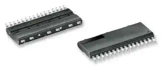
- IPM Case Style: SPM23-BA
- IPM Power Device: MOSFET
- Isolation Voltage: 1500Vrms
- Current Rating (Ic / Id): 3A
- Voltage Rating (Vces / Vdss): 500V
| Delivery and price | |
|---|---|
| Units per pack | 700 |
| Price | 5.51 € |
| Current stock | 10+ |
| Lead time | 30 days |
## **Is Now Part of** **To learn more about ON Semiconductor, please visit our website at www.onsemi.com** ON Semiconductor and the ON Semiconductor logo are trademarks of Semiconductor Components Industries, LLC dba ON Semiconductor or its subsidiaries in the United States and/or other countries. ON Semiconductor owns the rights to a number of patents, trademarks, copyrights, trade secrets, and other intellectual property. A listing of ON Semiconductor’s product/patent coverage may be accessed at www.onsemi.com/site/pdf/Patent-Marking.pdf. ON Semiconductor reserves the right to make changes without further notice to any products herein. ON Semiconductor makes no warranty, representation or guarantee regarding the suitability of its products for any particular purpose, nor does ON Semiconductor assume any liability arising out of the application or use of any product or circuit, and specifically disclaims any and all liability, including without limitation special, consequential or incidental damages. Buyer is responsible for its products and applications using ON Semiconductor products, including compliance with all laws, regulations and safety requirements or standards, regardless of any support or applications information provided by ON Semiconductor. “Typical” parameters which may be provided in ON Semiconductor data sheets and/or specifications can and do vary in different applications and actual performance may vary over time. All operating parameters, including “Typicals” must be validated for each customer application by customer’s technical experts. ON Semiconductor does not convey any license under its patent rights nor the rights of others. ON Semiconductor products are not designed, intended, or authorized for use as a critical component in life support systems or any FDA Class 3 medical devices or medical devices with a same or similar classification in a foreign jurisdiction or any devices intended for implantation in the human body. Should Buyer purchase or use ON Semiconductor products for any such unintended or unauthorized application, Buyer shall indemnify and hold ON Semiconductor and its officers, employees, subsidiaries, affiliates, and distributors harmless against all claims, costs, damages, and expenses, and reasonable attorney fees arising out of, directly or indirectly, any claim of personal injury or death associated with such unintended or unauthorized use, even if such claim alleges that ON Semiconductor was negligent regarding the design or manufacture of the part. ON Semiconductor is an Equal Opportunity/Affirmative Action Employer. This literature is subject to all applicable copyright laws and is not for resale in any manner. January 2014 ## **FSB50450S Motion SPM[®] 5 Series** ## **Features** - UL Certified No. E209204 (UL1557) - 500 V RDS(on) = 2.4 Max FRFET MOSFET 3-Phase Inverter with Gate Drivers - Separate Open-Source Pins from Low-Side MOSFETs for Three-Phase Current-Sensing - Active-HIGH Interface, Works with 3.3 / 5 V Logic, Schmitt-trigger Input - Optimized for Low Electromagnetic Interference - HVIC for Gate Driving and Under-Voltage Protection - Isolation Rating: 1500 Vrms / min. - Mosisture Sensitive Level (MSL) 3 - RoHS Compliant ## **Applications** - 3-Phase Inverter Driver for Small Power AC Motor Drives ## **Related Source** - _AN-9082 - Motion SPM5 Series Thermal Performance by Contact Pressure_ - _AN-9080 - User’s Guide for Motion SPM 5 Series Ver.1_ ## **General Description** The FSB50450S is an advanced Motion SPM **[®]** 5 module providing a fully-featured, high-performance inverter output stage for AC Induction, BLDC and PMSM motors. These modules integrate optimized gate drive of the built-in MOSFETs (FRFET **[®]** technology) to minimize EMI and losses. The built-in, high-speed HVIC requires only a single supply voltage and translates the incoming logic-level gate inputs to the high-voltage, high-current drive signals required to properly drive the module's internal MOSFETs. Separate open-source MOSFET terminals are available for each phase to support the widest variety of control algorithms. ## **Package Marking & Ordering Information** |**Device Marking**|**Device**|**Package**|**Reel Size**|**Packing Type**|**Quantity**| |---|---|---|---|---|---| |FSB50450S|FSB50450S|SPM5D-023|330mm|Tape-Reel|450| 1 ©2010 Fairchild Semiconductor Corporation FSB50450S Rev. C4 www.fairchildsemi.com ## **Absolute Maximum Ratings** **Inverter Part** (each MOSFET unless otherwise specified.) |**Symbol**|**Parameter**|**Conditions**|**Rating**|**Unit**| |---|---|---|---|---| |VDSS|Drain-Source Voltage of Each MOSFET||500|V| |*ID 25|Each MOSFET Drain Current, Continuous|TC= 25°C|1.5|A| |*ID 80|Each MOSFET Drain Current, Continuous|TC= 80°C|1.1|A| |*IDP|Each MOSFET Drain Current, Peak|TC= 25°C, PW < 100s|3.0|A| |*PD|Maximum Power Dissipation|TC= 25°C, For Each MOSFET|10|W| **Control Part** (each HVIC unless otherwise specified.) |**Symbol**|**Parameter**|**Conditions**|**Rating**|**Unit**| |---|---|---|---|---| |VCC|Control Supply Voltage|Applied Between VCCand COM|20|V| |VBS|High-side Bias Voltage|Applied Between VBand VS|20|V| |VIN|Input Signal Voltage|Applied Between IN and COM|-0.3 ~ VCC+ 0.3|V| |**Thermal Resistance**||||| |**Symbol**|**Parameter**|**Conditions**|**Rating**|**Unit**| |RJC|Junction to Case Thermal Resistance|Each MOSFET under Inverter Oper-<br>ating Condition (1st Note 1)|8.9|°C/W| |**Total System**||||| |**Symbol**|**Parameter**|**Conditions**|**Rating**|**Unit**| |TJ|Operating Junction Temperature||-20 ~ 150|°C| |TSTG|Storage Temperature||-50 ~ 150|°C| |VISO|Isolation Voltage|60 Hz, Sinusoidal, 1 Minute, Con-<br>nect Pins to Heat Sink Plate|1500|Vrms| ## **1st Notes:** 1. For the measurement point of case temperature TC, please refer to Figure 4. 2. Marking “ * “ is calculation value or design factor. 2 ©2010 Fairchild Semiconductor Corporation FSB50450S Rev. C4 www.fairchildsemi.com ## **Pin descriptions** |**Pin Number**|**Pin Name**|**Pin Description**| |---|---|---| |1|COM|IC Common Supply Ground| |2|VB(U)|Bias Voltage for U Phase High Side MOSFET Driving| |3|VCC(U)|Bias Voltage for U Phase IC and Low Side MOSFET Driving| |4|IN(UH)|Signal Input for U Phase High-Side| |5|IN(UL)|Signal Input for U Phase Low-Side| |6|VS(U)|Bias Voltage Ground for U Phase High Side MOSFET Driving| |7|VB(V)|Bias Voltage for V Phase High Side MOSFET Driving| |8|VCC(V)|Bias Voltage for V Phase IC and Low Side MOSFET Driving| |9|IN(VH)|Signal Input for V Phase High-Side| |10|IN(VL)|Signal Input for V Phase Low-Side| |11|VS(V)|Bias Voltage Ground for V Phase High Side MOSFET Driving| |12|VB(W)|Bias Voltage for W Phase High Side MOSFET Driving| |13|VCC(W)|Bias Voltage for W Phase IC and Low Side MOSFET Driving| |14|IN(WH)|Signal Input for W Phase High-Side| |15|IN(WL)|Signal Input for W Phase Low-Side| |16|VS(W)|Bias Voltage Ground for W Phase High Side MOSFET Driving| |17|P|Positive DC–Link Input| |18|U|Output for U Phase| |19|NU|Negative DC–Link Input for U Phase| |20|NV|Negative DC–Link Input for V Phase| |21|V|Output for V Phase| |22|NW|Negative DC–Link Input for W Phase| |23|W|Output for W Phase| |(1) COM<br>(2) VB(U)<br>(3) VCC(U)<br>(4) IN(UH)<br>(5) IN(UL)<br>(6) VS(U)<br>(7) VB(V)<br>(8) VCC(V)<br>(9) IN(VH)<br>(10) IN(VL)<br>(11) VS(V)<br>(12) VB(W)<br>(13) VCC(W)<br>(14) IN(WH)<br>(15) IN(WL)<br>(16) VS(W)||||||||(17) P<br>(18) U<br>(19) NU<br>(20) NV<br>(21) V<br>(22) NW<br>(23) W| |---|---|---|---|---|---|---|---|---| |||||||||| |||COM<br>VCC<br>LIN<br>HIN<br>VB<br>HO<br>VS<br>LO||||||| |||||||||| |||||||||| |||||||||| |||||||||| |||||||||| |||COM<br>VCC<br>LIN<br>HIN<br>VB<br>HO<br>VS<br>LO||||||| |||||||||| |||||||||| |||||||||| |||||||||| |||||||||| |||||||||| |||COM<br>VCC<br>LIN<br>HIN<br>VB<br>HO<br>VS<br>LO||||||| |||||||||| |||||||||| |||||||||| |||||||||| |||||||||| ## **Figure 1. Pin Configuration and Internal Block Diagram (Bottom View)** **1st Notes:** 3. Source terminal of each low-side MOSFET is not connected to supply ground or bias voltage ground inside Motion SPM[®] 5 product. External connections should be made as indicated in Figure 3. 3 ©2010 Fairchild Semiconductor Corporation FSB50450S Rev. C4 www.fairchildsemi.com **Electrical Characteristics** (TJ = 25°C, VCC = VBS = 15 V unless otherwise specified.) **Inverter Part** (each MOSFET unless otherwise specified.) |**Symbol**|**Parameter**|**Conditions**|**Conditions**|**Min**|**Typ**|**Max**|**Unit**| |---|---|---|---|---|---|---|---| |BVDSS|Drain - Source<br>Breakdown Voltage|VIN= 0 V, ID= 250A (2nd Note 1)||500|-|-|V| |IDSS|Zero Gate Voltage<br>Drain Current|VIN= 0 V, VDS= 500 V||-|-|250|A| |RDS(on)|Static Drain - Source<br>Turn-On Resistance|VCC= VBS= 15 V, VIN= 5 V, ID= 0.5 A||-|1.9|2.4|| |VSD|Drain - Source Diode<br>Forward Voltage|VCC= VBS= 15V, VIN= 0 V, ID= -0.5 A||-|-|1.2|V| |tON|Switching Times|VPN= 300 V, VCC= VBS= 15 V, ID= 0.5 A<br>VIN= 0 V5 V, Inductive Load L = 3 mH<br>High- and Low-Side MOSFET Switching<br>(2nd Note 2)||-|1152|-|ns| |tOFF||||-|600|-|ns| |trr||||-|185|-|ns| |EON||||-|85|-|J| |EOFF||||-|11|-|J| |RBSOA|Reverse Bias Safe Oper-<br>ating Area|VPN= 400 V, VCC= VBS= 15 V, ID= IDP, VDS= BVDSS,<br>TJ= 150°C<br>High- and Low-Side MOSFET Switching (2nd Note 3)||Full Square|||| |**Control Part**(each HVIC unless otherwise specified.)|||||||| |**Symbol**|**Parameter**|**Conditions**||**Min**|**Typ**|**Max**|**Unit**| |IQCC|Quiescent VCCCurrent|VCC= 15 V,<br>VIN= 0 V|Applied Between VCCand COM|-|-|160|A| |IQBS|Quiescent VBSCurrent|VBS= 15 V,<br>VIN= 0 V|Applied Between VB(U)- U,<br>VB(V)- V, VB(W)- W|-|-|100|A| |UVCCD|Low-Side Under-Voltage<br>Protection (Figure 8)|VCCUnder-Voltage Protection Detection Level||7.4|8.0|9.4|V| |UVCCR||VCCUnder-Voltage Protection Reset Level||8.0|8.9|9.8|V| |UVBSD|High-Side Under-Voltage<br>Protection (Figure 9)|VBSUnder-Voltage Protection Detection Level||7.4|8.0|9.4|V| |UVBSR||VBSUnder-Voltage Protection Reset Level||8.0|8.9|9.8|V| |VIH|ON Threshold Voltage|Logic HIGH Level|Applied between IN and COM|3.0|-|-|V| |VIL|OFF Threshold Voltage|Logic LOW Level||-|-|0.8|V| |IIH|Input Bias Current|VIN= 5 V|Applied between IN and COM|-|10|20|A| |IIL||VIN= 0 V||-|-|2|A| ## **2nd Notes:** 1. BVDSS is the absolute maximum voltage rating between drain and source terminal of each MOSFET inside Motion SPM[®] 5 product. VPN should be sufficiently less than this value considering the effect of the stray inductance so that VPN should not exceed BVDSS in any case. 2. tON and tOFF include the propagation delay of the internal drive IC. Listed values are measured at the laboratory test condition, and they can be different according to the field applications due to the effect of different printed circuit boards and wirings. Please see Figure 4 for the switching time definition with the switching test circuit of Figure 5. 3. The peak current and voltage of each MOSFET during the switching operation should be included in the Safe Operating Area (SOA). Please see Figure 5 for the RBSOA test circuit that is same as the switching test circuit. 4 ©2010 Fairchild Semiconductor Corporation FSB50450S Rev. C4 www.fairchildsemi.com ## **Recommended Operating Condition** |**Symbol**|**Parameter**|**Conditions**|**Min.**|**Typ.**|**Max.**|**Unit**| |---|---|---|---|---|---|---| |VPN|Supply Voltage<br>Applied Betw|een P and N|-|300|400|V| |VCC|Control Supply Voltage<br>Applied Betw|een VCCand COM|13.5|15.0|16.5|V| |VBS|High-Side Bias Voltage<br>Applied Betw|een VBand VS|13.5|15.0|16.5|V| |VIN(ON)|Input ON Threshold Voltage<br>Applied Betw<br>Input OFF Threshold Voltage|een IN and COM|3.0|-|VCC|V| |VIN(OFF)|||0|-|0.6|V| |tdead|Blanking Time for Preventing<br>Arm-Short<br>VCC= VBS=|13.5 ~ 16.5 V, TJ 150°C|1|-|-|s| |fPWM|PWM Switching Frequency<br>TJ 150°C||-|15|-|kHz| |TC|Case Temperature<br>TJ 150°C||-20|-|100|°C| **==> picture [465 x 158] intentionally omitted <==** **----- Start of picture text -----**<br> These values depend on PWM<br>control algorithm<br>15-V Line R2<br>R1 D1 P VDC<br>HIN LIN Output Note<br>R5 VCCHIN HOVB Inverter Output 0 0 Z Both FRFET Off<br>Micom 0 1 0 Low side FRFET On<br>LIN VS C3 1 0 VDC High side FRFET On<br>C5 COM LO<br>N R3 1 1 Forbidden Shoot through<br>Open Open Z Same as (0,0)<br>10F C2 C1 One-Leg Diagram of SPM [?] 5 Product<br>* Example of bootstrap paramters:<br> C1 = C2 = 1F ceramic capacitor,<br> R1 = 56 R2 = 20<br>**----- End of picture text -----**<br> ## **Figure 2. Recommended MCU Interface and Bootstrap Circuit with Parameters** ## **3rd Notes:** 1. It is recommended the bootstrap diode D1 to have soft and fast recovery characteristics with 600 V Rating. 2. Parameters for bootstrap circuit elements are dependent on PWM algorithm. For 15 kHz of switching frequency, typical example of parameters is shown above. 3. RC-coupling (R5 and C5) and C4 at each input of Motion SPM 5 product and MCU (Indicated as Dotted Lines) may be used to prevent improper signal due to surge-noise. 4. Bold lines should be short and thick in PCB pattern to have small stray inductance of circuit, which results in the reduction of surge-voltage. Bypass capacitors such as C1, C2 and C3 should have good high-frequency characteristics to absorb high-frequency ripple-current. **==> picture [271 x 150] intentionally omitted <==** **----- Start of picture text -----**<br> 14.50mm<br>3.80mm<br>MOSFET Case Temperature(Tc)<br>Detecting Point<br>Figure 3. Case Temperature Measurement<br>**----- End of picture text -----**<br> ## **3rd Notes:** 5. Attach the thermocouple on top of the heat-sink of SPM 5 package (between SPM 5 package and heatsink if applied) to get the correct temperature measurement. 5 ©2010 Fairchild Semiconductor Corporation FSB50450S Rev. C4 www.fairchildsemi.com **==> picture [370 x 303] intentionally omitted <==** **----- Start of picture text -----**<br> VIN VIN<br>Irr<br>100% of ID 120% of ID<br>VDS ID<br>10% of ID<br>ID VDS<br>tON trr tOFF<br>(a) Turn-on (b) Turn-off<br>Figure 4. Switching Time Definitions<br>REH<br>VCC ID<br>RBS<br>VCC VB<br>L VDC<br>HIN HO<br>LIN VS<br>+<br>COM LO VDS<br>-<br>CBS One-leg Diagram of Motion SPM [®] 5 Product<br>**----- End of picture text -----**<br> **Figure 5. Switching and RBSOA (Single-pulse) Test Circuit (Low-side)** **==> picture [310 x 284] intentionally omitted <==** **----- Start of picture text -----**<br> Input Signal<br>UV Protection<br>RESET DETECTION RESET<br>Status<br>Low-side Supply, VCC UVCCD UVCCR<br>MOSFET Current<br>Figure 6. Under-Voltage Protection (Low-Side)<br>Input Signal<br>UV Protection<br>RESET DETECTION RESET<br>Status<br>High-side Supply, VBS UVBSD UVBSR<br>MOSFET Current<br>**----- End of picture text -----**<br> **Figure 7. Under-Voltage Protection (High-Side)** 6 ©2010 Fairchild Semiconductor Corporation FSB50450S Rev. C4 www.fairchildsemi.com **==> picture [461 x 356] intentionally omitted <==** **----- Start of picture text -----**<br> R2<br>(1) COM<br>R1 (2) VB(U) (17) P<br>(3) VCC(U) VCC VB<br>R5 (4) IN(UH) HIN HO (18) U<br>(5) IN(UL) LIN VS<br>RC1 5 C2 C 1 (6) V(7) VS(U)B(V) COM LO (19) NU C3 VDC<br>(8) VCC(V) VCC VB (20) NV<br>(9) IN(VH) HIN HO (21) V<br>(10) IN(VL) LIN VS M<br>C2 C 1 (11) VS(V) COM LO<br>R1 (12) VB(W)<br>(13) VCC(W) VCC VB (22) NW<br>(14) IN(WH) HIN HO (23) W<br>(15) IN(WL) LIN VS<br>C2 C 1 (16) VS(W) COM LO<br>For 3-phase current sensing and protection R4<br>15-V<br>Supply C4 R3<br>Micom<br>**----- End of picture text -----**<br> ## **Figure 8. Example of Application Circuit** ## **4th Notes:** 1. About pin position, refer to Figure 1. 2. RC-coupling (R5 and C5, R4 and C6) and C4 at each input of Motion SPM[®] 5 product and MCU are useful to prevent improper input signal caused by surge-noise. 3. The voltage-drop across R3 affects the low-side switching performance and the bootstrap characteristics since it is placed between COM and the source terminal of the lowside MOSFET. For this reason, the voltage-drop across R3 should be less than 1 V in the steady-state. 4. Ground-wires and output terminals, should be thick and short in order to avoid surge-voltage and malfunction of HVIC. 5. All the filter capacitors should be connected close to Motion SPM 5 product, and they should have good characteristics for rejecting high-frequency ripple current. 7 ©2010 Fairchild Semiconductor Corporation FSB50450S Rev. C4 www.fairchildsemi.com ## **Detailed Package Outline Drawings** _Package drawings are provided as a service to customers considering Fairchild components. Drawings may change in any manner without notice. Please note the revision and/or data on the drawing and contact a FairchildSemiconductor representative to verify or obtain the most recent revision. Package specifications do not expand the terms of Fairchild’s worldwide therm and conditions, specifically the the warranty therein, which covers Fairchild products._ _Always visit Fairchild Semiconductor’s online packaging area for the most recent package drawings:_ _http://www.fairchildsemi.com/dwg/MO/MOD23DE.pdf_ 8 ©2010 Fairchild Semiconductor Corporation FSB50450S Rev. C4 www.fairchildsemi.com ©2010 Fairchild Semiconductor Corporation 9 FSB50450S Rev. C4 www.fairchildsemi.com ON Semiconductor and are trademarks of Semiconductor Components Industries, LLC dba ON Semiconductor or its subsidiaries in the United States and/or other countries. ON Semiconductor owns the rights to a number of patents, trademarks, copyrights, trade secrets, and other intellectual property. A listing of ON Semiconductor’s product/patent coverage may be accessed at www.onsemi.com/site/pdf/Patent−Marking.pdf. ON Semiconductor reserves the right to make changes without further notice to any products herein. ON Semiconductor makes no warranty, representation or guarantee regarding the suitability of its products for any particular purpose, nor does ON Semiconductor assume any liability arising out of the application or use of any product or circuit, and specifically disclaims any and all liability, including without limitation special, consequential or incidental damages. Buyer is responsible for its products and applications using ON Semiconductor products, including compliance with all laws, regulations and safety requirements or standards, regardless of any support or applications information provided by ON Semiconductor. “Typical” parameters which may be provided in ON Semiconductor data sheets and/or specifications can and do vary in different applications and actual performance may vary over time. All operating parameters, including “Typicals” must be validated for each customer application by customer’s technical experts. ON Semiconductor does not convey any license under its patent rights nor the rights of others. ON Semiconductor products are not designed, intended, or authorized for use as a critical component in life support systems or any FDA Class 3 medical devices or medical devices with a same or similar classification in a foreign jurisdiction or any devices intended for implantation in the human body. Should Buyer purchase or use ON Semiconductor products for any such unintended or unauthorized application, Buyer shall indemnify and hold ON Semiconductor and its officers, employees, subsidiaries, affiliates, and distributors harmless against all claims, costs, damages, and expenses, and reasonable attorney fees arising out of, directly or indirectly, any claim of personal injury or death associated with such unintended or unauthorized use, even if such claim alleges that ON Semiconductor was negligent regarding the design or manufacture of the part. ON Semiconductor is an Equal Opportunity/Affirmative Action Employer. This literature is subject to all applicable copyright laws and is not for resale in any manner. ## **PUBLICATION ORDERING INFORMATION** **N. American Technical Support** : 800−282−9855 Toll Free **ON Semiconductor Website** : **www.onsemi.com** USA/Canada ## **LITERATURE FULFILLMENT** : Literature Distribution Center for ON Semiconductor **Order Literature** : http://www.onsemi.com/orderlit For additional information, please contact your local Sales Representative 19521 E. 32nd Pkwy, Aurora, Colorado 80011 USA **Europe, Middle East and Africa Technical Support: Phone** : 303−675−2175 or 800−344−3860 Toll Free USA/Canada Phone: 421 33 790 2910 **Fax** : 303−675−2176 or 800−344−3867 Toll Free USA/Canada **Japan Customer Focus Center Email** : orderlit@onsemi.com Phone: 81−3−5817−1050 © Semiconductor Components Industries, LLC www.onsemi.com **www.onsemi.com** **1**
Updated at February 9, 2023
onsemi is a premier global supplier of intelligent power and sensing technologies, driving disruptive innovations across the automotive, industrial, and cloud infrastructure markets. Recognized for their commitment to sustainability and reliable supply chains, the company accelerates advancements in vehicle electrification, industrial automation, and 5G networks by solving the industry's most complex design challenges. At the core of their portfolio is an industry-leading selection of discrete semiconductors. This extensive range features thousands of high-performance bipolar transistors, single and dual MOSFETs, and a comprehensive array of diodes, including Zener, Schottky, and fast-recovery rectifiers. Engineered for superior thermal performance and energy efficiency, these foundational components are critical for demanding power conversion, switching, and signal conditioning applications. Beyond essential discretes, onsemi provides a robust suite of advanced power management and circuit protection solutions. Their lineup includes intelligent power modules, single IGBTs, and transient voltage suppression (TVS) diodes designed to safeguard sensitive circuitry. Complimented by integrated passive filters, AC/DC LED driver ICs, and specialized sub-2.4GHz RF transceivers, onsemi equips engineers with the scalable, high-quality technologies needed to build a cleaner, smarter, and more connected world.
About Novapart
Novapart is a B2B electronic component broker specialising in stock shortages and cost reduction. We source hard-to-find parts and identify compliant alternatives across a catalogue of 410,000+ components from 500+ manufacturers.
Learn more →Stock Shortage Specialist
When a component is unavailable, discontinued or has an unacceptable lead time, we tap into our network of vetted European and Asian distributors to source what you need — without compromising on quality or traceability.
Request a quote →Compliant Alternatives
We identify pin-to-pin, electrically equivalent substitutes that meet the same certifications (RoHS, AEC-Q100, REACH) as your original specification — validated against datasheets, not just part numbers. Often at a lower cost.
BOM Analysis service →