
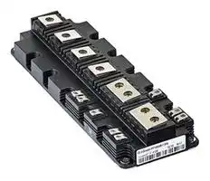


FR900R12IP4DBPSA1
IGBT Module, Dual, Brake-Chopper, 900 A, 1.7 V, 150 °C, Module
- Manufacturer: INFINEON
- Product type: IGBT Modules
- SVHC: No SVHC (25-Jun-2025)
- Product Range: PrimePACK 3
- IGBT Technology: IGBT 4 [Trench/Field Stop]
- IGBT Termination: Tab
- Power Dissipation: -
- IGBT Configuration: Dual, Brake-Chopper
- Transistor Mounting: Panel
- DC Collector Current: 900A
- Power Dissipation Pd: -
- Transistor Case Style: Module
- Operating Temperature Max: 150°C
- Junction Temperature Tj Max: 150°C
- Continuous Collector Current: 900A
- Collector Emitter Voltage Max: 1.2kV
- Collector Emitter Voltage V(br)ceo: 1.2kV
- Collector Emitter Saturation Voltage: 1.7V
- Collector Emitter Saturation Voltage Vce(on): 1.7V
| Delivery and price | |
|---|---|
| Units per pack | 1 |
| Price | 801.62 € |
| Current stock | 10+ |
| Lead time | 30 days |
## FR900R12IP4D

VCES = 1200V IC nom = 900A / ICRM = 1800A

- Chopper-Anwendungen

-

- Hybrid-Nutzfahrzeuge

- Motorantriebe

-

-

- CEsat

- T

- VCEsat

-

-

-

-

-

-

-

-

-

-

-

-

-

-

- CEsat

- T vj op

- • VCEsat

-

-

-

-

-

-

-

-

**Digit**

Datasheet www.infineon.com

2019-07-12

FR900R12IP4D

**==> picture [86 x 38] intentionally omitted <==**

## **IGBT,�Brems-Chopper�/�IGBT,�Brake-Chopper Höchstzulässige�Werte�/�Maximum�Rated�Values**

|Kollektor-Emitter-Sperrspannung<br>Collector-emittervoltage|Tvj= 25°C|VCES|1200|1200||V|
|---|---|---|---|---|---|---|
|Kollektor-Dauergleichstrom<br>ContinuousDCcollectorcurrent|TC= 100°C, Tvj max= 175°C|ICDC|900|||A|
|PeriodischerKollektor-Spitzenstrom<br>Repetitivepeakcollectorcurrent|tP= 1 ms|ICRM|1800|||A|
|Gate-Emitter-Spitzenspannung<br>Gate-emitterpeakvoltage||VGES|+/-20|||V|
|**CharakteristischeWerte/CharacteristicValues**|||min.|typ.|max.||
|Kollektor-Emitter-Sättigungsspannung<br>Collector-emittersaturationvoltage|IC= 900 A<br>VGE= 15 V<br>Tvj= 25°C<br>Tvj= 125°C<br>Tvj= 150°C|VCE sat||1,70<br>2,00<br>2,10|2,05<br>2,40|V<br>V<br>V|
|Gate-Schwellenspannung<br>Gatethresholdvoltage|IC= 33,0 mA, VCE= VGE, Tvj= 25°C|VGEth|5,00|5,80|6,50|V|
|Gateladung<br>Gatecharge|VGE= -15 / 15 V|QG||6,40||µC|
|InternerGatewiderstand<br>Internalgateresistor|Tvj= 25°C|RGint||1,2||Ω|
|Eingangskapazität<br>Inputcapacitance|f = 1000 kHz, Tvj= 25°C, VCE= 25 V, VGE= 0 V|Cies||54,0||nF|
|Rückwirkungskapazität<br>Reversetransfercapacitance|f = 1000 kHz, Tvj= 25°C, VCE= 25 V, VGE= 0 V|Cres||2,80||nF|
|Kollektor-Emitter-Reststrom<br>Collector-emittercut-offcurrent|VCE= 1200 V, VGE= 0 V, Tvj= 25°C|ICES|||5,0|mA|
|Gate-Emitter-Reststrom<br>Gate-emitterleakagecurrent|VCE= 0 V, VGE= 20 V, Tvj= 25°C|IGES|||400|nA|
|Einschaltverzögerungszeit,induktiveLast<br>Turn-ondelaytime,inductiveload|IC= 900 A, VCE= 600 V<br>VGE= -15 / 15 V<br>RGon= 1,2Ω<br>Tvj= 25°C<br>Tvj= 125°C<br>Tvj= 150°C|td on||0,23<br>0,26<br>0,27||µs<br>µs<br>µs|
|Anstiegszeit,induktiveLast<br>Risetime,inductiveload|IC= 900 A, VCE= 600 V<br>VGE= -15 / 15 V<br>RGon= 1,2Ω<br>Tvj= 25°C<br>Tvj= 125°C<br>Tvj= 150°C|tr||0,10<br>0,11<br>0,11||µs<br>µs<br>µs|
|Abschaltverzögerungszeit,induktiveLast<br>Turn-offdelaytime,inductiveload|IC= 900 A, VCE= 600 V<br>VGE= -15 / 15 V<br>RGoff= 1,2Ω<br>Tvj= 25°C<br>Tvj= 125°C<br>Tvj= 150°C|td off||0,60<br>0,70<br>0,73||µs<br>µs<br>µs|
|Fallzeit,induktiveLast<br>Falltime,inductiveload|IC= 900 A, VCE= 600 V<br>VGE= -15 / 15 V<br>RGoff= 1,2Ω<br>Tvj= 25°C<br>Tvj= 125°C<br>Tvj= 150°C|tf||0,14<br>0,16<br>0,17||µs<br>µs<br>µs|
|EinschaltverlustenergieproPuls<br>Turn-onenergylossperpulse|IC= 900 A, VCE= 600 V, Lσ= 45 nH<br>di/dt = 7800 A/µs (Tvj= 150°C)<br>VGE= -15 / 15 V, RGon= 1,2Ω<br>Tvj= 25°C<br>Tvj= 125°C<br>Tvj= 150°C|Eon||53,0<br>83,0<br>93,0||mJ<br>mJ<br>mJ|
|AbschaltverlustenergieproPuls<br>Turn-offenergylossperpulse|IC= 900 A, VCE= 600 V, Lσ= 45 nH<br>du/dt = 2700 V/µs (Tvj= 150°C)<br>VGE= -15 / 15 V, RGoff= 1,2Ω<br>Tvj= 25°C<br>Tvj= 125°C<br>Tvj= 150°C|Eoff||140<br>185<br>200||mJ<br>mJ<br>mJ|
|Kurzschlußverhalten<br>SCdata|VGE ≤15 V, VCC= 800 V<br>VCEmax= VCES-LsCE·di/dt<br>Tvj= 150°C<br>tP ≤10 µs,|ISC||3600||A|
|Wärmewiderstand,ChipbisGehäuse<br>Thermalresistance,junctiontocase|proIGBT/perIGBT|RthJC|||29,6|K/kW|
|Wärmewiderstand,GehäusebisKühlkörper<br>Thermalresistance,casetoheatsink|proIGBT/perIGBT<br>λPaste=1W/(m·K)/λgrease=1W/(m·K)|RthCH||13,9||K/kW|
|TemperaturimSchaltbetrieb<br>Temperatureunderswitchingconditions||Tvj op|-40||150|°C|


2

V�3.0 2019-07-12

Datasheet

FR900R12IP4D

**==> picture [86 x 38] intentionally omitted <==**

## **Diode,�Brems-Chopper�/�Diode,�Brake-Chopper Höchstzulässige�Werte�/�Maximum�Rated�Values**

|PeriodischeSpitzensperrspannung<br>Repetitivepeakreversevoltage|Tvj= 25°C|VRRM|1200|1200||V|
|---|---|---|---|---|---|---|
|Dauergleichstrom<br>ContinuousDCforwardcurrent||IF|900|||A|
|PeriodischerSpitzenstrom<br>Repetitivepeakforwardcurrent|tP= 1 ms|IFRM|1800|||A|
|Grenzlastintegral<br>I²t-value|VR= 0 V, tP= 10 ms, Tvj= 125°C<br>VR= 0 V, tP= 10 ms, Tvj= 150°C|I²t|91,0<br>88,0|||kA²s<br>kA²s|
|**CharakteristischeWerte/CharacteristicValues**|||min.|typ.|max.||
|Durchlassspannung<br>Forwardvoltage|IF= 900 A, VGE= 0 V<br>IF= 900 A, VGE= 0 V<br>IF= 900 A, VGE= 0 V<br>Tvj= 25°C<br>Tvj= 125°C<br>Tvj= 150°C|VF||1,65<br>1,55<br>1,50|2,15<br>2,00|V<br>V<br>V|
|Rückstromspitze<br>Peakreverserecoverycurrent|IF= 900 A, - diF/dt = 7800 A/µs (Tvj=150°C)<br>VR= 600 V<br>VGE= -15 V<br>Tvj= 25°C<br>Tvj= 125°C<br>Tvj= 150°C|IRM||560<br>750<br>800||A<br>A<br>A|
|Sperrverzögerungsladung<br>Recoveredcharge|IF= 900 A, - diF/dt = 7800 A/µs (Tvj=150°C)<br>VR= 600 V<br>VGE= -15 V<br>Tvj= 25°C<br>Tvj= 125°C<br>Tvj= 150°C|Qr||89,0<br>180<br>210||µC<br>µC<br>µC|
|AbschaltenergieproPuls<br>Reverserecoveryenergy|IF= 900 A, - diF/dt = 7800 A/µs (Tvj=150°C)<br>VR= 600 V<br>VGE= -15 V<br>Tvj= 25°C<br>Tvj= 125°C<br>Tvj= 150°C|Erec||43,0<br>87,0<br>100||mJ<br>mJ<br>mJ|
|Wärmewiderstand,ChipbisGehäuse<br>Thermalresistance,junctiontocase|proDiode/perdiode|RthJC|||44,2|K/kW|
|Wärmewiderstand,GehäusebisKühlkörper<br>Thermalresistance,casetoheatsink|proDiode/perdiode<br>λPaste=1W/(m·K)/λgrease=1W/(m·K)|RthCH||12,4||K/kW|
|TemperaturimSchaltbetrieb<br>Temperatureunderswitchingconditions||Tvj op|-40||150|°C|
|**Diode,Revers/Diode,Reverse**<br>**HöchstzulässigeWerte/MaximumRatedValues**|||||||
|PeriodischeSpitzensperrspannung<br>Repetitivepeakreversevoltage|Tvj= 25°C|VRRM|1200|||V|
|Dauergleichstrom<br>ContinuousDCforwardcurrent||IF|150|||A|
|PeriodischerSpitzenstrom<br>Repetitivepeakforwardcurrent|tP= 1 ms|IFRM|300|||A|
|Grenzlastintegral<br>I²t-value|VR= 0 V, tP= 10 ms, Tvj= 125°C|I²t|0,17|||kA²s|
|**CharakteristischeWerte/CharacteristicValues**|||min.|typ.|max.||
|Durchlassspannung<br>Forwardvoltage|IF= 150 A, VGE= 0 V<br>IF= 150 A, VGE= 0 V<br>Tvj= 25°C<br>Tvj= 125°C|VF||1,65<br>1,65|2,15|V<br>V|
|Wärmewiderstand,ChipbisGehäuse<br>Thermalresistance,junctiontocase|proDiode/perdiode|RthJC|||225|K/kW|
|Wärmewiderstand,GehäusebisKühlkörper<br>Thermalresistance,casetoheatsink|proDiode/perdiode<br>λPaste=1W/(m·K)/λgrease=1W/(m·K)|RthCH||120||K/kW|
|TemperaturimSchaltbetrieb<br>Temperatureunderswitchingconditions||Tvj op|-40||150|°C|


3

V�3.0 2019-07-12

Datasheet

FR900R12IP4D

**==> picture [86 x 38] intentionally omitted <==**

## **NTC-Widerstand�/�NTC-Thermistor**

|**NTC-Widerstand/NTC-Thermistor**|**NTC-Widerstand/NTC-Thermistor**||||||
|---|---|---|---|---|---|---|
|**CharakteristischeWerte/CharacteristicValues**|||min.|typ.|max.||
|Nennwiderstand<br>Ratedresistance|TNTC= 25°C|R25||5,00||kΩ|
|AbweichungvonR100<br>DeviationofR100|TNTC= 100°C, R100= 493Ω|∆R/R|-5||5|%|
|Verlustleistung<br>Powerdissipation|TNTC= 25°C|P25|||20,0|mW|
|B-Wert<br>B-value|R2= R25exp [B25/50(1/T2- 1/(298,15 K))]|B25/50||3375||K|
|B-Wert<br>B-value|R2= R25exp [B25/80(1/T2- 1/(298,15 K))]|B25/80||3411||K|
|B-Wert<br>B-value|R2= R25exp [B25/100(1/T2- 1/(298,15 K))]|B25/100||3433||K|


Angaben�gemäß�gültiger�Application�Note. Specification�according�to�the�valid�application�note.

## **Modul�/�Module**

|**Modul/Module**|||||||
|---|---|---|---|---|---|---|
|Isolations-Prüfspannung<br>Isolationtestvoltage|RMS, f = 50 Hz, t = 1 min.|VISOL|4,0<br>|||kV|
|MaterialModulgrundplatte<br>Materialofmodulebaseplate|||Cu||||
|InnereIsolation<br>Internalisolation|Basisisolierung(Schutzklasse1,EN61140)<br>basicinsulation(class1,IEC61140)||Al2O3||||
|Kriechstrecke<br>Creepagedistance|Kontakt-Kühlkörper/terminaltoheatsink<br>Kontakt-Kontakt/terminaltoterminal||33,0<br>33,0<br>|||mm|
|Luftstrecke<br>Clearance|Kontakt-Kühlkörper/terminaltoheatsink<br>Kontakt-Kontakt/terminaltoterminal||19,0<br>19,0<br>|||mm|
|VergleichszahlderKriechwegbildung<br>Comperativetrackingindex||CTI||> 400|||
||||min.|typ.|max.||
|Modulstreuinduktivität<br>Strayinductancemodule||LsCE||10||nH|
|Modulleitungswiderstand,Anschlüsse-<br>Chip<br>Moduleleadresistance,terminals-chip|TC=25°C,proSchalter/perswitch|RCC'+EE'||0,23||mΩ|
|Lagertemperatur<br>Storagetemperature||Tstg|-40||150|°C|
|Anzugsdrehmomentf.Modulmontage<br>Mountingtorqueformodulmounting|SchraubeM5-Montagegem.gültigerApplikationsschrift<br>ScrewM5-Mountingaccordingtovalidapplicationnote|M|3,00||6,00|Nm|
|Anzugsdrehmomentf.elektr.Anschlüsse<br>Terminalconnectiontorque|SchraubeM4-Montagegem.gültigerApplikationsschrift<br>ScrewM4-Mountingaccordingtovalidapplicationnote<br>SchraubeM8-Montagegem.gültigerApplikationsschrift<br>ScrewM8-Mountingaccordingtovalidapplicationnote|M|1,8<br>8,0|-<br>-|2,1<br>10|Nm<br>Nm|
|Gewicht<br>Weight||G||1400||g|


V�3.0 2019-07-12

Datasheet

4

FR900R12IP4D

**==> picture [86 x 38] intentionally omitted <==**

**Ausgangskennlinie�IGBT,�Brems-Chopper�(typisch) output�characteristic�IGBT,�Brake-Chopper�(typical)** IC�=�f�(VCE) VGE�=�15�V

**==> picture [237 x 282] intentionally omitted <==**

**----- Start of picture text -----**<br>
1800<br>Tvj = 25°C<br>1600 T T vj vj  = 125°C  = 150 ° C<br>1400<br>1200<br>1000<br>800<br>600<br>400<br>200<br>0<br>0,0 0,5 1,0 1,5 2,0 2,5 3,0 3,5<br>VCE [V]<br> [A]<br>IC<br>**----- End of picture text -----**<br>


**Ausgangskennlinienfeld�IGBT,�Brems-Chopper�(typisch) output�characteristic�IGBT,�Brake-Chopper�(typical)** IC�=�f�(VCE) Tvj�=�150°C

**==> picture [237 x 282] intentionally omitted <==**

**----- Start of picture text -----**<br>
1800<br>VGE = 19V<br>VGE = 17V<br>1600 VGE = 15V<br>VGE = 13V<br>VGE = 11V<br>VGE = 9V<br>1400<br>1200<br>1000<br>800<br>600<br>400<br>200<br>0<br>0,0 0,5 1,0 1,5 2,0 2,5 3,0 3,5 4,0 4,5 5,0<br>VCE [V]<br> [A]<br>IC<br>**----- End of picture text -----**<br>


**Übertragungscharakteristik�IGBT,�Brems-Chopper�(typisch) transfer�characteristic�IGBT,�Brake-Chopper�(typical)** IC�=�f�(VGE) VCE�=�20�V

**Schaltverluste�IGBT,�Brems-Chopper�(typisch) switching�losses�IGBT,�Brake-Chopper�(typical)** Eon�=�f�(IC),�Eoff�=�f�(IC)

VGE�=�±15�V,�RGon�=�1.2� Ω ,�RGoff�=�1.2� Ω ,�VCE�=�600�V

**==> picture [487 x 282] intentionally omitted <==**

**----- Start of picture text -----**<br>
1800 400<br>Tvj = 25°C Eon, Tvj = 125°C<br>1600 T T vj vj  = 125°C  = 150 ° C EEonoff, T, Tvjvj = 150°C = 125°C<br>350 Eoff, Tvj = 150°C<br>1400<br>300<br>1200<br>250<br>1000<br>200<br>800<br>150<br>600<br>100<br>400<br>50<br>200<br>0 0<br>5 6 7 8 9 10 11 12 0 200 400 600 800 1000 1200 1400 1600 1800<br>VGE [V] IC [A]<br> [A]<br>IC E [mJ]<br>**----- End of picture text -----**<br>


V�3.0 2019-07-12

Datasheet

5

FR900R12IP4D

**==> picture [486 x 656] intentionally omitted <==**

**----- Start of picture text -----**<br>
Eon =f(R),E G off =f(R G) ZthJC =f (t)<br>VGE =+15V,1 C =900A,V CE =600V<br>600 100 pot TT<br>550 E E on on , T , T vj vj  = 125°C  = 150 ° C ZthJC : IGBT<br>Eoff, Tvj = 125°C<br>500 Eoff, Tvj = 150°C 7 J [.] |<br>450<br>400<br>350<br>300 10<br>250<br>200<br>150 4<br>y<br>y<br>100<br>i: 1 2 3 4<br>ri[K/kW]: 1,49 2,68 20,7 4,76<br>50 τ i[s]: 0,0000652 0,000951 0,0403 0,311<br>y, CCS<br>0 1<br>0,0 2,0 4,0 6,0 8,0 10,0 12,0 0,001 0,01 0,1 1 10<br>RG [ Ω ] t [s]<br>Sicherer Riickw.-Arbeitsber. IGBT, Brems-Chopper (RBSOA) Durchlasskennlinie der Diode, Brems-Chopper (typisch)<br>reverse bias safe operating area IGBT, Brake-Chopper forward characteristic of Diode, Brake-Chopper (typical)<br>(RBSOA) IF =f(V F)<br>IC =f(V CE)<br>VGE =415V,R Goff =1.2 Ω ,T vj =150°C<br>2000 1800<br>IICC, Modul, Chip TTvjvj = 25°C = 125°C<br>1800 1620 T vj  = 150°C<br>1600 1440<br>/<br>i<br>i<br>1400 1260<br>1200 1080<br>1000 900<br>/<br>i<br>//<br>800 720 it<br>//<br>600 540 |<br>/<br>//<br>1<br>400 360<br>200 180<br>0 0<br>0 200 400 600 800 1000 1200 1400 0,0 0,5 1,0 1,5 2,0 2,5<br>VCE  [V] VF [V]<br>[K/kW]<br>E [mJ]<br>thJC<br>Z<br> [A]  [A]<br>IC IF<br>**----- End of picture text -----**<br>


6

Datasheet

2019-07-12

FR900R12IP4D

**==> picture [488 x 309] intentionally omitted <==**

**----- Start of picture text -----**<br>
Erec =f (I F) Erec =f(R G)<br>RGon =1.2 Ω ,V CE =600V IF =900A,V CE =600V<br>140 140<br>Erec, Tvj = 125°C Erec, Tvj = 125°C<br>130 E rec , T vj  = 150°C 130 E rec , T vj  = 150°C<br>120 120<br>110 110 RAR<br>\<br>100 100 \<br>\<br>90 90<br>80 80<br>70 70<br>60 ao/4aeee 60 Nees ~“<br>50 50<br>40 40<br>30 30<br>20 / 20 Ht =<br>10 10<br>0 0<br>0 200 400 600 800 1000 1200 1400 1600 1800 0,0 2,0 4,0 6,0 8,0 10,0 12,0<br>IF [A] RG [ Ω ]<br>E [mJ] E [mJ]<br>**----- End of picture text -----**<br>


ZthJC

**==> picture [485 x 282] intentionally omitted <==**

**----- Start of picture text -----**<br>
100 100000<br>It ZthJC : Diode ——— Rtyp<br>i | a OO<br>EL | ea<br>10000<br>10<br>1000<br>i: 1 2 3 4<br>ri[K/kW]: 5,03 4,97 26,8 7,41<br>τ i[s]: 0,000162 0,00199 0,0397 0,305<br>1 100<br>0,001 0,01 0,1 1 10 0 20 40 60 80 100 120 140 160<br>t [s] TNTC [°C]<br>] Ω<br> [K/kW] R[<br>thJC<br>Z<br>**----- End of picture text -----**<br>


Datasheet

7

2019-07-12

FR900R12IP4D

**==> picture [86 x 38] intentionally omitted <==**

## **Schaltpla** ~~**n**~~ **�/�Circuit�diagram**

**==> picture [189 x 153] intentionally omitted <==**

**----- Start of picture text -----**<br>
11, 13<br>5<br>4<br>9 10<br>3 8<br>6<br>1<br>�<br>2<br>7<br>12, 14<br>**----- End of picture text -----**<br>


## **Gehäuseabmessungen�/�Package�outlines**

**==> picture [494 x 324] intentionally omitted <==**

**----- Start of picture text -----**<br>
36 [�] [0,2]  (2x) 8 [�] [0,1]  (8x) 18 [�] [0,2]  (4x)<br>250 [�] [1]<br>A<br>224<br>187<br>recommended design height lower side 150<br>bus bar to baseplate 113<br>76<br>38,25 [�] [0,25] screwing depthmax. 8mm (8x) 24 58 M8 (8x) � � 0,8 A B C � 5,5 -0,2 (14x) � � 0,5 A B C<br>7,5 + 0,5 6 8x 14x<br>max. 3<br>screwing depth<br>max. 16mm (8x)<br>max. 2 26 [�] [0,25] B 14( � 5,5) M4 (8x) � 8x � 0,8 A B C ( � 5,5) C<br>recommended design height lower side 25<br>PCB to baseplate 39<br>64<br>78<br>92<br>103<br>117<br>156<br>195<br>234<br>10 (6x)<br>23,60,3  � 73 890,5  �<br>37 39<br>0,3  �  (2x)  (2x)<br>3,8 (8x) 20,6 0,3  � 0,3  �<br>25,1 22,1<br> (8x)<br>11,80,3  �<br>**----- End of picture text -----**<br>


8

V�3.0 2019-07-12

Datasheet

## **Trademarks**

## **WARNHINWEIS**

## **WARNINGS**
Updated at April 28, 2026
Infineon Technologies is a globally recognized leader in semiconductor solutions, renowned for driving innovation in power management, energy efficiency, and modern mobility. With a strong legacy of engineering excellence, the company provides highly reliable components designed to meet the rigorous demands of industrial, automotive, and advanced commercial applications. The core of our Infineon portfolio is centered on their industry-leading discrete semiconductors. We offer an extensive selection of single and dual MOSFETs, alongside a robust range of single IGBTs and advanced IGBT modules. These flagship power transistors are essential for high-efficiency power conversion and motor control, providing engineers with superior thermal performance and minimized switching losses. Beyond advanced field-effect transistors, the selection includes a comprehensive array of diodes and rectifiers, heavily featuring Schottky diodes, as well as fast-recovery and RF/PIN diodes. This power foundation is further supported by bipolar transistors, intelligent power modules, and thyristor SCR modules, delivering the critical building blocks required for complex power system designs. To support broader system integration, the portfolio also encompasses specialized solutions such as solid-state relays, AC/DC LED driver ICs, and Bluetooth communications modules. From high-power industrial rectifiers to wireless connectivity adapters, Infineon equips designers with the precision components needed to build efficient, scalable, and fully connected electronic systems.
About Novapart
Novapart is a B2B electronic component broker specialising in stock shortages and cost reduction. We source hard-to-find parts and identify compliant alternatives across a catalogue of 410,000+ components from 500+ manufacturers.
Learn more →Stock Shortage Specialist
When a component is unavailable, discontinued or has an unacceptable lead time, we tap into our network of vetted European and Asian distributors to source what you need — without compromising on quality or traceability.
Request a quote →Compliant Alternatives
We identify pin-to-pin, electrically equivalent substitutes that meet the same certifications (RoHS, AEC-Q100, REACH) as your original specification — validated against datasheets, not just part numbers. Often at a lower cost.
BOM Analysis service →