


FPDB40PH60B
Intelligent Power Module (IPM), IGBT, 600 V, 40 A, 2.5 kV, SPMGC-027, SPM3
- Manufacturer: ONSEMI
- Product type: Intelligent Power Modules
- SVHC: No SVHC (25-Jun-2025)
- IPM Series: SPM3
- Product Range: PFC SPM 3 Series
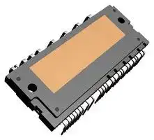
- IPM Case Style: SPMGC-027
- IPM Power Device: IGBT
- Isolation Voltage: 2.5kV
- Current Rating (Ic / Id): 40A
- Voltage Rating (Vces / Vdss): 600V
| Delivery and price | |
|---|---|
| Units per pack | 250 |
| Price | 10.61 € |
| Current stock | 50+ |
| Lead time | 30 days |
## **Is Now Part of** ## **To learn more about ON Semiconductor, please visit our website at www.onsemi.com** Please note: As part of the Fairchild Semiconductor integration, some of the Fairchild orderable part numbers will need to change in order to meet ON Semiconductor’s system requirements. Since the ON Semiconductor product management systems do not have the ability to manage part nomenclature that utilizes an underscore (_), the underscore (_) in the Fairchild part numbers will be changed to a dash (-). This document may contain device numbers with an underscore (_). Please check the ON Semiconductor website to verify the updated device numbers. The most current and up-to-date ordering information can be found at www.onsemi.com. Please email any questions regarding the system integration to Fairchild_questions@onsemi.com. ON Semiconductor and the ON Semiconductor logo are trademarks of Semiconductor Components Industries, LLC dba ON Semiconductor or its subsidiaries in the United States and/or other countries. ON Semiconductor owns the rights to a number of patents, trademarks, copyrights, trade secrets, and other intellectual property. A listing of ON Semiconductor’s product/patent coverage may be accessed at www.onsemi.com/site/pdf/Patent-Marking.pdf. ON Semiconductor reserves the right to make changes without further notice to any products herein. ON Semiconductor makes no warranty, representation or guarantee regarding the suitability of its products for any particular purpose, nor does ON Semiconductor assume any liability arising out of the application or use of any product or circuit, and specifically disclaims any and all liability, including without limitation special, consequential or incidental damages. Buyer is responsible for its products and applications using ON Semiconductor products, including compliance with all laws, regulations and safety requirements or standards, regardless of any support or applications information provided by ON Semiconductor. “Typical” parameters which may be provided in ON Semiconductor data sheets and/or specifications can and do vary in different applications and actual performance may vary over time. All operating parameters, including “Typicals” must be validated for each customer application by customer’s technical experts. ON Semiconductor does not convey any license under its patent rights nor the rights of others. ON Semiconductor products are not designed, intended, or authorized for use as a critical component in life support systems or any FDA Class 3 medical devices or medical devices with a same or similar classification in a foreign jurisdiction or any devices intended for implantation in the human body. Should Buyer purchase or use ON Semiconductor products for any such unintended or unauthorized application, Buyer shall indemnify and hold ON Semiconductor and its officers, employees, subsidiaries, affiliates, and distributors harmless against all claims, costs, damages, and expenses, and reasonable attorney fees arising out of, directly or indirectly, any claim of personal injury or death associated with such unintended or unauthorized use, even if such claim alleges that ON Semiconductor was negligent regarding the design or manufacture of the part. ON Semiconductor is an Equal Opportunity/Affirmative Action Employer. This literature is subject to all applicable copyright laws and is not for resale in any manner. **==> picture [65 x 8] intentionally omitted <==** **----- Start of picture text -----**<br> December 2013<br>**----- End of picture text -----**<br> ## **FPDB40PH60B** ## **PFC SPM[®] 3 Series for 2-Phase Bridgeless PFC** ## **Features** - UL Certified No. E209204 (UL1557) - 600 V - 40 A 2-Phase Bridgeless PFC with Integral Gate Driver and Protection - Very Low Thermal Resistance Using Al2O3 DBC Substrate - Built-in NTC Thermistor for Temperature Monitoring - Built-in Shunt Resistor for Current Sensing - Optimized for 20kHz Switching Frequency - Isolation Rating: 2500 Vrms/min. ## **Applications** ## **General Description** The FPDB40PH60B is an advanced PFC SPM[®] 3 module providing a fully-featured, high-performance Bridgeless PFC (Power Factor Correction) input power stage for consumer, medical, and industrial applications. These modules integrate optimized gate drive of the built-in IGBTs to minimize EMI and losses, while also providing multiple on-module protection features including under-voltage lockout, over-current shutdown, thermal monitoring, and fault reporting. These modules also feature high-performance output diodes and shunt resistor for additional space savings and mounting convenience. - 2-Phase Bridgeless PFC Converter ## **Related Source** - _AN-9041 - Bridgeless PFC SPM 3 Series Design Guide_ **Figure 1. Package Overview** ## **Package Marking & Ordering Information** |**Device**|**Device Marking**|**Package**|**Packing Type**|**Quantity**| |---|---|---|---|---| |FPDB40PH60B|FPDB40PH60B|SPMGC-027|Rail|10| 1 ©2011 Fairchild Semiconductor Corporation FPDB40PH60B Rev. C3 www.fairchildsemi.com ## **Integrated Drive, Protection and System Control Functions** - For IGBTs: gate drive circuit, Over-Current Protection (OCP), control supply circuit Under-Voltage Lock-Out (UVLO) Protection - Fault signal: corresponding to OC and UV fault - Built-in thermistor: temperature monitoring - Input interface: active-HIGH interface, works with 3.3 / 5 V logic, Schmitt-trigger input ## **Pin Configuration** **==> picture [397 x 281] intentionally omitted <==** **----- Start of picture text -----**<br> (1) VCC(L)<br>(2) COM (21) VAC-<br>(3) NC<br>(4) IN(R) (22) NSENSE<br>(5) IN(S)<br>(6) VFO (23) NC<br>(7) CFOD<br>(8) CSC<br>(9) NC<br>(24) N<br>(10) NC<br>(11) NC Case Temperature (T C)<br>Detecting Point<br>(12) NC<br>(13) NC (25) R<br>(14) NC<br>(15) NC<br>(16) NC<br>(26) S<br>(17) NC<br>(18) NC DBC Substrate<br>(19) RTH<br>(27) PR<br>(20) VTH<br>**----- End of picture text -----**<br> **Figure 2. Top View** 2 ©2011 Fairchild Semiconductor Corporation FPDB40PH60B Rev. C3 www.fairchildsemi.com ## **Pin Descriptions** |**Pin Number**|**Pin Name**|**Pin Description**| |---|---|---| |1|VCC|Common Bias Voltage for IC and IGBTs Driving| |2|COM|Common Supply Ground| |4|IN(R)|Signal Input for Low-Side R-Phase IGBT| |5|IN(S)|Signal Input for Low-Side S-Phase IGBT| |6|VFO|Fault Output| |7|CFOD|Capacitor for Fault Output Duration Selection| |8|CSC|Capacitor(Low-Pass Filter) for Over-Current Detection| |19|R(TH)|Series Resistor for The Use of Thermistor| |20|V(TH)|Thermistor Bias Voltage| |21|VAC-|Current Sensing Terminal| |22|NSENSE|Current Sensing Reference Terminal| |24|N|Negative Rail of DC-Link| |25|R|Output for R-Phase| |26|S|Output for S-Phase| |27|PR|Positive Rail of DC-Link| |3, 9~18, 23|NC|No Connection| ## **Internal Equivalent Circuit** |(20) VTH<br>(19) RTH<br>(8) CSC<br>(7) CFOD<br>(6) VFO<br>(5) IN(S)<br>(4) IN(R)<br>(2) COM<br>(1) VCC|CSC<br>CFOD<br>VFO<br>IN(S)<br>IN(R)<br>COM<br>VCC<br>OUT(S)<br>OUT(R)<br>NTC<br>Thermistor|Q1|Shunt<br>Resistor<br>Q2<br>D1<br>D3<br>D2<br>D4|Shunt<br>Resistor<br>Q2<br>D1<br>D3<br>D2<br>D4|(27) PR<br>(26) S<br>(25) R<br>(23) NC<br>(22) NSENSE<br>(21) VAC-<br>(24) N| |---|---|---|---|---|---| ||||D1||| ||||Q2<br>D3||| ||||||| ||||||| ||||||| ## **Figure 3. Internal Block Diagram** ## **Notes:** 1. Converter is composed of two IGBTs including four diodes and one IC which has gate driving and protection functions. 3 ©2011 Fairchild Semiconductor Corporation FPDB40PH60B Rev. C3 www.fairchildsemi.com ## **Absolute Maximum Ratings** (TJ = 25°C, unless otherwise specified.) **Converter Part** |**Symbol**|**Item**|**Condition**|**Rating**|**Unit**| |---|---|---|---|---| |Vi|Supply Voltage|Applied between R - S|264|Vrms| |Vi(Surge)|Supply Voltage (Surge)|Applied between R - S|500|V| |VPN|Output Voltage|Applied between P - N|450|V| |VPN(Surge)|Output Voltage (Surge)|Applied between P - N|500|V| |VCES|Collector - Emitter Voltage||600|V| |±IC|Each IGBT Collector Current|TC= 25°C|40|A| |±ICP|Each IGBT Collector Current (Peak)|TC= 25°C, Under 1 ms Pulse Width|70|A| |PC|Collector Dissipation|TC= 25°C per IGBT|113|W| |VRRM|Repetitive Peak Reverse Voltage||600|V| |IFSM|Peak Forward Surge Current|Single Half Sine-Wave|350|A| |PRSH|Power Rating of Shunt Resistor|TC< 125°C|2|W| |TJ|Operating Junction Temperature|(Note 2)|-40 ~ 150|°C| **Notes:** 2. The maximum junction temperature rating of the power chips integrated within the PFC SPM **[®]** product is 150°C(@TC ≤ 100°C). ## **Control Part** |**Symbol**|**Item**|**Condition**|**Rating**|**Unit**| |---|---|---|---|---| |VCC|Control Supply Voltage|Applied between VCC- COM|20|V| |VIN|Input Signal Voltage|Applied between IN - COM|-0.3 ~ 17.0|V| |VFO|Fault Output Supply Voltage|Applied between VFO- COM|-0.3 ~ VCC+0.3|V| |IFO|Fault Output Current|Sink Current at VFOPin|5|mA| |VSC|Current Sensing Input Voltage|Applied between CSC- COM|-0.3~VCC+0.3|V| ## **Total System** |**Symbol**|**Item**|**Condition**|**Condition**|**Condition**|**Rating**|**Rating**|**Unit**|**Unit**| |---|---|---|---|---|---|---|---|---| |TC|Module Case Operation Temperature||||-20 ~ 100||°C|| |TSTG|Storage Temperature||||-40 ~ 150||°C|| |VISO|Isolation Voltage|60 Hz, Sinusoidal, AC 1 Minute, Connect<br>Pins to Heat-Sink Plate|||2500||Vrms|| |**Thermal Resistance**||||||||| |**Symbol**|**Item**|**Condition**|**Min.**|**Typ.**||**Max.**||**Unit**| |R(j-c)Q|Junction to Case Thermal Resistance<br>(Referenced to PKG Center)|IGBT|-|-||1.1||°C/W| |R(j-c)HD||High-Side Diode|-|-||1.9||°C/W| |R(j-c)LD||Low-Side Diode|-|-||1.4||°C/W| ## **Notes:** 3. For the measurement point of case temperature(TC), please refer to Figure 2. 4 ©2011 Fairchild Semiconductor Corporation FPDB40PH60B Rev. C3 www.fairchildsemi.com ## **Electrical Characteristics** (TJ = 25°C, unless otherwise specified.) ## **Converter Part** |**Symbol**|**Item**|**Condition**|**Min.**|**Typ.**|**Max.**|**Unit**| |---|---|---|---|---|---|---| |VCE(SAT)|IGBT Saturation Voltage|VCC= 15 V, VIN= 5 V, IC= 40 A|-|1.8|2.3|V| |VFH|High-Side Diode Voltage|IF= 40 A|-|2.2|2.7|V| |VFL|Low-Side Diode Voltage|IF= 40 A|-|1.15|1.55|V| |tON|Switching Times|VPN= 400 V, VCC= 15 V, IC= 40 A<br>VIN= 0 V5 V, Inductive Load<br>(Note 4)|-|500|-|ns| |tC(ON)|||-|180|-|ns| |tOFF|||-|500|-|ns| |tC(OFF)|||-|90|-|ns| |trr|||-|43|-|ns| |Irr|||-|6|-|A| |RSENSE|Current-Sensing resistor||1.8|2.0|2.2|m| |ICES|Collector - Emitter<br>Leakage Current|VCE= VCES|-|-|250|A| - **Notes:** 4. tON and tOFF include the propagation delay of the internal drive IC. tC(ON) and tC(OFF) are the switching time of IGBT itself under the given gate driving condition internally. For the detailed information, please see Figure 4. **==> picture [451 x 176] intentionally omitted <==** **----- Start of picture text -----**<br> Irr<br>100% of IC 120% of IC<br>VCE IC<br>90% of I C<br>10% of VCE 10% of IC<br>IC 10% of IC VCE 10% of VCE<br>VIN VIN<br>tON trr tC(OFF)<br>tC(ON) tOFF<br>(a) Turn-on (b) Turn-off<br>**----- End of picture text -----**<br> **Figure 4. Switching Time Definition** 5 ©2011 Fairchild Semiconductor Corporation FPDB40PH60B Rev. C3 www.fairchildsemi.com ## **Control Part** |**Symbol**|**Item**|**Item**|**Condition**|**Condition**|**Condition**|**Condition**|**Condition**|**Condition**|**Condition**|**Condition**|**Condition**|**Condition**|**Min.**|**Typ.**|**Max.**|**Unit**| |---|---|---|---|---|---|---|---|---|---|---|---|---|---|---|---|---| |IQCCL|Quiescent VCCSupply Current||VCC= 15 V, IN = 0 V|||||VCC- COM|||||-|-|26|mA| |VFOH|Fault Output Voltage||VSC= 0 V, VFOCircuit: 4.7 kto 5 V Pull-up||||||||||4.5|-|-|V| |VFOL|||VSC= 1 V, VFOCircuit: 4.7 kto 5 V Pull-up||||||||||-|-|0.8|V| |VSC(ref)|Over-Current Trip Level||VCC= 15 V||||||||||0.45|0.50|0.55|V| |UVCCD|Supply Circuit Under-Voltage<br>Protection||Detection Level||||||||||10.7|11.9|13.0|V| |UVCCR|||Reset Level||||||||||11.2|12.4|13.2|V| |tFOD|Fault-Out Pulse Width||CFOD= 33 nF (Note 5)||||||||||1.4|1.8|2.0|ms| |VIN(ON)|ON Threshold Voltage||Applied between IN - COM||||||||||3.0|-|-|V| |VIN(OFF)|OFF Threshold Voltage||||||||||||-|-|0.8|V| |RTH|Resistance of Thermistor||at TC= 25°C (See Figure 5)||||||||||-|50|-|k| ||||at TC= 80°C (See Figure 5)||||||||||-|5.76|-|k| |**Notes:**<br>5. The fault-out pulse width tFODdepends on the capacitance value of CFODaccording to the following approximate equation : CFOD= 18.3 x 10⁻⁶x tFOD[F]<br>**Figure 5. R-T Curve of the Built-in Thermistor**<br>R-T Graph<br>0<br>20<br>40<br>60<br>80<br>100<br>120<br>20<br>30<br>40<br>50<br>60<br>70<br>80<br>90<br>100 110 120 130<br>Temperature [C]<br>Resistance [k]||acitance va||||||||||||||| |||||||||||||||||| |||||||||||||||||| |||||||||||||||||| |||||||||||||||||| |||||||||||||||||| |||||||||||||||||| |||||||||||||||||| ## **Recommended Operating conditions** |**Symbol**|**Item**|**Condition**|**Min.**|**Typ.**|**Max.**|**Unit**| |---|---|---|---|---|---|---| |VI|Input Supply Voltage|Applied between R - S|180|-|264|Vrms| |VPN|Output Voltage|Applied between P - N|-|280|400|V| |VCC|Control Supply Voltage|Applied between VCC- COM|13.5|15|16.5|V| |dVCC/dt|Control Supply Variation|<br>Applied between IN - COM|-1|-|1|V/s| |fPWM|PWM Input Signal|TC 100°C, TJ 125°C, per IGBT|-|20|-|kHz| 6 ©2011 Fairchild Semiconductor Corporation FPDB40PH60B Rev. C3 www.fairchildsemi.com ## **Mechanical Characteristics and Ratings** |**Item**|**Condition**|**Condition**|**Min.**|**Typ.**|**Max.**|**Units**| |---|---|---|---|---|---|---| |Mounting Torque|Mounting Screw: M3<br>R|ecommended 0.62 N•m|0.51|0.62|0.72|N•m| |Device Flatness|See Figure 6||0|-|+120|m| |Weight|||-|15.00|-|g| **==> picture [206 x 153] intentionally omitted <==** **----- Start of picture text -----**<br> (+)<br>(+)<br>(+)<br>**----- End of picture text -----**<br> **Figure 6. Flatness Measurement Position** 7 ©2011 Fairchild Semiconductor Corporation FPDB40PH60B Rev. C3 www.fairchildsemi.com ## **Time Charts of Protective Function** **==> picture [334 x 190] intentionally omitted <==** **----- Start of picture text -----**<br> Input Signal<br>Internal IGBT<br>P3<br>Gate-Em itter Voltage<br>UV<br>P5<br>reset<br>Control Supply Voltage UV P2<br>detect<br>P6<br>P1<br>Output Current<br>Fault Output Signal P4<br>**----- End of picture text -----**<br> P1 : Normal operation: IGBT ON and conducting current. P2 : Under-voltage detection. P3 : IGBT gate interrupt. P4 : Fault signal generation. P5 : Under-voltage reset. P6 : Normal operation: IGBT ON and conducting current. **Figure 7. Under-Voltage Protection** **==> picture [361 x 235] intentionally omitted <==** **----- Start of picture text -----**<br> P 5<br>In p u t S ig n a l<br>P 6<br>Inte rn a l IG B T<br>G a te -E m itte r V o lta g e<br>O C D ete ctio n<br>P 1<br>P 4<br>O u tp u t C u rre n t P 7<br>P 2<br>O C R efe re nce<br>V olta ge (0 .5V )<br>S e n sin g V o lta ge<br>R C F ilte r D ela y<br>P 8<br>F a u lt O u tp u t S ig n a l P 3<br>**----- End of picture text -----**<br> P1 : Normal operation: IGBT ON and conducting current. P2 : Over current detection. P3 : IGBT gate interrupt / fault signal generation. P4 : IGBT is slowly turned off. P5 : IGBT OFF signal. P6 : IGBT ON signal: but IGBT cannot be turned on during the fault output activation. P7 : IGBT OFF state. P8 : Fault output reset and normal operation start. ## **Figure 8. Over-Current Protection** 8 ©2011 Fairchild Semiconductor Corporation FPDB40PH60B Rev. C3 www.fairchildsemi.com **==> picture [451 x 262] intentionally omitted <==** **----- Start of picture text -----**<br> Vac<br>+5 V<br>VTH<br>RTH ThermistorNTC PR<br>CSC CSC S<br>MCU CFOD CFOD R<br>VFO VFO 3-Phase Inverter<br>or<br>IN(S) IN(S) OUT(S)<br>Controller IN(R) IN(R) N<br>COM OUT(R) Shunt NSENSE<br>COM Resistor<br>VCC VCC VAC-<br>**----- End of picture text -----**<br> **Figure 9. Application Example** ## **Notes:** 6. For the over-current protection, please set time constant in the range 3 ~ 4 s. 9 ©2011 Fairchild Semiconductor Corporation FPDB40PH60B Rev. C3 www.fairchildsemi.com ## **Detailed Package Outline Drawings** _Package drawings are provided as a service to customers considering Fairchild components. Drawings may change in any manner without notice. Please note the revision and/or data on the drawing and contact a FairchildSemiconductor representative to verify or obtain the most recent revision. Package specifications do not expand the terms of Fairchild’s worldwide therm and conditions, specifically the the warranty therein, which covers Fairchild products._ _Always visit Fairchild Semiconductor’s online packaging area for the most recent package drawings:_ _http://www.fairchildsemi.com/dwg/MO/MOD27BA.pdf_ 10 ©2011 Fairchild Semiconductor Corporation FPDB40PH60B Rev. C3 www.fairchildsemi.com ©2011 Fairchild Semiconductor Corporation 11 FPDB40PH60B Rev. C3 www.fairchildsemi.com ON Semiconductor and are trademarks of Semiconductor Components Industries, LLC dba ON Semiconductor or its subsidiaries in the United States and/or other countries. ON Semiconductor owns the rights to a number of patents, trademarks, copyrights, trade secrets, and other intellectual property. A listing of ON Semiconductor’s product/patent coverage may be accessed at www.onsemi.com/site/pdf/Patent−Marking.pdf. ON Semiconductor reserves the right to make changes without further notice to any products herein. ON Semiconductor makes no warranty, representation or guarantee regarding the suitability of its products for any particular purpose, nor does ON Semiconductor assume any liability arising out of the application or use of any product or circuit, and specifically disclaims any and all liability, including without limitation special, consequential or incidental damages. Buyer is responsible for its products and applications using ON Semiconductor products, including compliance with all laws, regulations and safety requirements or standards, regardless of any support or applications information provided by ON Semiconductor. “Typical” parameters which may be provided in ON Semiconductor data sheets and/or specifications can and do vary in different applications and actual performance may vary over time. All operating parameters, including “Typicals” must be validated for each customer application by customer’s technical experts. ON Semiconductor does not convey any license under its patent rights nor the rights of others. ON Semiconductor products are not designed, intended, or authorized for use as a critical component in life support systems or any FDA Class 3 medical devices or medical devices with a same or similar classification in a foreign jurisdiction or any devices intended for implantation in the human body. Should Buyer purchase or use ON Semiconductor products for any such unintended or unauthorized application, Buyer shall indemnify and hold ON Semiconductor and its officers, employees, subsidiaries, affiliates, and distributors harmless against all claims, costs, damages, and expenses, and reasonable attorney fees arising out of, directly or indirectly, any claim of personal injury or death associated with such unintended or unauthorized use, even if such claim alleges that ON Semiconductor was negligent regarding the design or manufacture of the part. ON Semiconductor is an Equal Opportunity/Affirmative Action Employer. This literature is subject to all applicable copyright laws and is not for resale in any manner. ## **PUBLICATION ORDERING INFORMATION** **N. American Technical Support** : 800−282−9855 Toll Free **ON Semiconductor Website** : **www.onsemi.com** USA/Canada ## **LITERATURE FULFILLMENT** : Literature Distribution Center for ON Semiconductor **Order Literature** : http://www.onsemi.com/orderlit For additional information, please contact your local Sales Representative 19521 E. 32nd Pkwy, Aurora, Colorado 80011 USA **Europe, Middle East and Africa Technical Support: Phone** : 303−675−2175 or 800−344−3860 Toll Free USA/Canada Phone: 421 33 790 2910 **Fax** : 303−675−2176 or 800−344−3867 Toll Free USA/Canada **Japan Customer Focus Center Email** : orderlit@onsemi.com Phone: 81−3−5817−1050 © Semiconductor Components Industries, LLC www.onsemi.com **www.onsemi.com** **1**
Updated at April 27, 2026
onsemi is a premier global supplier of intelligent power and sensing technologies, driving disruptive innovations across the automotive, industrial, and cloud infrastructure markets. Recognized for their commitment to sustainability and reliable supply chains, the company accelerates advancements in vehicle electrification, industrial automation, and 5G networks by solving the industry's most complex design challenges. At the core of their portfolio is an industry-leading selection of discrete semiconductors. This extensive range features thousands of high-performance bipolar transistors, single and dual MOSFETs, and a comprehensive array of diodes, including Zener, Schottky, and fast-recovery rectifiers. Engineered for superior thermal performance and energy efficiency, these foundational components are critical for demanding power conversion, switching, and signal conditioning applications. Beyond essential discretes, onsemi provides a robust suite of advanced power management and circuit protection solutions. Their lineup includes intelligent power modules, single IGBTs, and transient voltage suppression (TVS) diodes designed to safeguard sensitive circuitry. Complimented by integrated passive filters, AC/DC LED driver ICs, and specialized sub-2.4GHz RF transceivers, onsemi equips engineers with the scalable, high-quality technologies needed to build a cleaner, smarter, and more connected world.
About Novapart
Novapart is a B2B electronic component broker specialising in stock shortages and cost reduction. We source hard-to-find parts and identify compliant alternatives across a catalogue of 410,000+ components from 500+ manufacturers.
Learn more →Stock Shortage Specialist
When a component is unavailable, discontinued or has an unacceptable lead time, we tap into our network of vetted European and Asian distributors to source what you need — without compromising on quality or traceability.
Request a quote →Compliant Alternatives
We identify pin-to-pin, electrically equivalent substitutes that meet the same certifications (RoHS, AEC-Q100, REACH) as your original specification — validated against datasheets, not just part numbers. Often at a lower cost.
BOM Analysis service →