


FNB81560T3
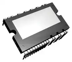
Intelligent Power Module (IPM), 3-Phase, IGBT, 600 V, 15 A, 1500 Vrms, SPMFA-A, SPM8
- Manufacturer: ONSEMI
- Product type: Intelligent Power Modules
- IPM Series: SPM8
- Product Range: Motion SPM® 8 Series
- IPM Case Style: SPMFA-A
- Isolation Voltage: 1500Vrms
- Current Rating (Ic / Id): 15A
| Delivery and price | |
|---|---|
| Units per pack | 100 |
| Price | 11.54 € |
| Current stock | 100+ |
| Lead time | 7 days |
## **Is Now Part of** ## **To learn more about ON Semiconductor, please visit our website at www.onsemi.com** Please note: As part of the Fairchild Semiconductor integration, some of the Fairchild orderable part numbers will need to change in order to meet ON Semiconductor’s system requirements. Since the ON Semiconductor product management systems do not have the ability to manage part nomenclature that utilizes an underscore (_), the underscore (_) in the Fairchild part numbers will be changed to a dash (-). This document may contain device numbers with an underscore (_). Please check the ON Semiconductor website to verify the updated device numbers. The most current and up-to-date ordering information can be found at www.onsemi.com. Please email any questions regarding the system integration to Fairchild_questions@onsemi.com. ON Semiconductor and the ON Semiconductor logo are trademarks of Semiconductor Components Industries, LLC dba ON Semiconductor or its subsidiaries in the United States and/or other countries. ON Semiconductor owns the rights to a number of patents, trademarks, copyrights, trade secrets, and other intellectual property. A listing of ON Semiconductor’s product/patent coverage may be accessed at www.onsemi.com/site/pdf/Patent-Marking.pdf. ON Semiconductor reserves the right to make changes without further notice to any products herein. ON Semiconductor makes no warranty, representation or guarantee regarding the suitability of its products for any particular purpose, nor does ON Semiconductor assume any liability arising out of the application or use of any product or circuit, and specifically disclaims any and all liability, including without limitation special, consequential or incidental damages. Buyer is responsible for its products and applications using ON Semiconductor products, including compliance with all laws, regulations and safety requirements or standards, regardless of any support or applications information provided by ON Semiconductor. “Typical” parameters which may be provided in ON Semiconductor data sheets and/or specifications can and do vary in different applications and actual performance may vary over time. All operating parameters, including “Typicals” must be validated for each customer application by customer’s technical experts. ON Semiconductor does not convey any license under its patent rights nor the rights of others. ON Semiconductor products are not designed, intended, or authorized for use as a critical component in life support systems or any FDA Class 3 medical devices or medical devices with a same or similar classification in a foreign jurisdiction or any devices intended for implantation in the human body. Should Buyer purchase or use ON Semiconductor products for any such unintended or unauthorized application, Buyer shall indemnify and hold ON Semiconductor and its officers, employees, subsidiaries, affiliates, and distributors harmless against all claims, costs, damages, and expenses, and reasonable attorney fees arising out of, directly or indirectly, any claim of personal injury or death associated with such unintended or unauthorized use, even if such claim alleges that ON Semiconductor was negligent regarding the design or manufacture of the part. ON Semiconductor is an Equal Opportunity/Affirmative Action Employer. This literature is subject to all applicable copyright laws and is not for resale in any manner. July 2017 ## **FNB81560T3 Motion SPM[®] 8 Series** ## **Features** - UL Certified No. E209204 (UL1557) - 600 V - 15 A 3-Phase IGBT Inverter Including Control IC for Gate Drive and Protections - Low-Loss, Short-Circuit Rated IGBTs - Separate Open-Emitter Pins from Low-Side IGBTs for Three-Phase Current Sensing - Active-high interface, works with 3.3 / 5 V Logic, Schmitt-trigger Input - HVIC for Gate Driving, Under-Voltage and Short-Circuit Current Protection - Fault Output for Under-Voltage and Short-Circuit Current Protection - Inter-Lock Function to Prevent Short-Circuit ## **General Description** FNB81560T3 is a Motion SPM 8 module providing a fully-featured, high-performance inverter output stage for AC Induction, BLDC, and PMSM motors. These modules integrate optimized gate drive of the built-in IGBTs to minimize EMI and losses, while also providing multiple on-module protection features including under-voltage lockouts, inter-lock function, over-current shutdown, thermal monitoring of drive IC, and fault reporting. The built-in, high-speed HVIC requires only a single supply voltage and translates the incoming logic-level gate inputs to the high-voltage, high-current drive signals required to properly drive the module's robust shortcircuit-rated IGBTs. Separate negative IGBT terminals are available for each phase to support the widest variety of control algorithms. - Shut-Down Input - HVIC Temperature-Sensing Built-In for Temperature Monitoring - Isolation Rating: 1500 Vrms / min. ## **Applications** - Motion Control - Home Appliance / Industrial Motor ## **Related Resources** - _AN-9112 - Smart Power Module, Motion SPM[®] 8 Series User’s Guide._ - _AN-9548 - SPM[®] 8 Pakage Assembly Guidance for 25L double DIP._ **SPMFA-A25** **Figure 1. 3D Package Drawing (Click to Activate 3D Content)** **Package Marking and Ordering Information Device Device Marking Package Packing Type Quantity** FNB81560T3 NB81560T3 SPMFA-A25 RAIL 15 ~~ee~~ 1 www.fairchildsemi.com ©2017 Semiconductor 1 www.onsemi.comFNB81560T3 Rev. 1.0 ## **Integrated Power Functions** - 600 V - 15 A IGBT inverter for three phase DC / AC power conversion ( _Please refer to Figure 3_ ) ## **Integrated Drive, Protection and System Control Functions** - For inverter high-side IGBTs: gate drive circuit, high-voltage isolated high-speed level shifting control circuit Under-Voltage Lock-Out (UVLO) protection Note: Available bootstrap circuit example is given in Figures 5 and 17 - control circuit Under-Voltage Lock-Out (UVLO) protection - For inverter low-side IGBTs: gate drive circuit, Over Curent Pretection(OCP), Short-Circuit Protection (SCP) control supply circuit Under-Voltage Lock-Out (UVLO) protection - Fault signaling: corresponding to UVLO (low-side supply) and SC faults - Input interface: High-active interface, works with 3.3 / 5 V logic, Schmitt trigger input ## **Pin Configuration** **==> picture [366 x 219] intentionally omitted <==** **----- Start of picture text -----**<br> (25) VBU<br>(1) P<br>(24) COM<br>(23) INUH<br>(2) U, VSU (22) INUL<br>(21) VDD<br>Case temperature (Tc)<br>(20) /SDU<br>Detecting point<br>(3) NU =<br>(19) VBV<br>(4) V, VSV (18) INVH<br>(17) INVL<br>(16) VDD<br>(5) NV E (15) /SDV<br>(<br>(14) VBW<br>(<br>(13) INWH<br>(12) INWL<br>(6) W, VSW (11) VDD<br>(10) Csc<br>(9) /FO,/SDW,VTS<br>(7) NW (8) COM<br>**----- End of picture text -----**<br> **Figure 2. Top View** www.onsemi.com[[FNB81560T3 Rev. 1.0]] 2 ©2017 Semiconductor www.fairchildsemi.com > [[FNB81560T3 Rev. 1.0]] ## **Pin Descriptions** |**Pin Number**|**Pin Name**|**Pin Description**| |---|---|---| |1|P|Positive DC-Link Input| |2|U, VSU|Output for U Phase| |3|NU|Negative DC-Link Input for U Phase| |4|V, VSV|Output for V Phase| |5|NV|Negative DC-Link Input for V Phase| |6|W, VSW|Output for W Phase| |7|NW|Negative DC-Link Input for W Phase| |8|COM|Common Supply Ground| |9|/FO, /SDW, VTS|Fault Output, Shut-Down Input for W Phase, Temperature Output of Drive IC| |10|CSC|Shut Down Input for Over Current and Short Circuit Protection| |11|VDD|Common Bias Voltage for IC and IGBTs Driving| |12|INWL|Signal Input for Low-Side W Phase| |13|INWH|Signal Input for High-Side W Phase| |14|VBW|High-Side Bias Voltage for W-Phase IGBT Driving| |15|/SDV|Shut-Down Input for V Phase| |16|VDD|Common Bias Voltage for IC and IGBTs Driving| |17|INVL|Signal Input for Low-Side V Phase| |18|INVH|Signal Input for High-Side V Phase| |19|VBV|High-Side Bias Voltage for V-Phase IGBT Driving| |20|/SDU|Shut-Down Input for U Phase| |21|VDD|Common Bias Voltage for IC and IGBTs Driving| |22|INUL|Signal Input for Low-Side U Phase| |23|INUH|Signal Input for High-Side U Phase| |24|COM|Common Supply Ground| |25|VBU|High-Side Bias Voltage for U-Phase IGBT Driving| www.onsemi.comFNB81560T3 Rev. 1.0 3 ©2017 Semiconductor FNB81560T3 Rev. 1.0 www.fairchildsemi.com ## **Internal Equivalent Circuit and Input/Output Pins** **==> picture [237 x 302] intentionally omitted <==** **----- Start of picture text -----**<br> P<br>VBU VB<br>INUH HIN HO<br>INUL LIN U,VSU<br>VDD VS<br>/SDU /SDVDDU<br>COM COM LO<br>NU<br>INVBVHV VBHIN HO<br>INVL<br>LIN V,VSV<br>VDD VDD VS<br>/SDV /SDV<br>COM LO<br>Nv<br>VBW VB<br>INWH HIN HO<br>INWL LIN<br>VDD W,VSW<br>VDD VS<br>Csc Csc<br>/FO, /SDW, VTS<br>COM COM/FO, /SDW, VTS LO<br>Nw<br>**----- End of picture text -----**<br> ## **Figure 3. Internal Block Diagram** ## **Note:** 1. Inverter high-side is composed of three IGBTs, freewheeling diodes. 2. Inverter low-side is composed of three IGBTs, freewheeling diodes. 3. Inverter power side is composed of four inverter DC-link input terminals and three inverter output terminals. www.onsemi.comFNB81560T3 Rev. 1.0 4 ©2017 Semiconductor FNB81560T3 Rev. 1.0 www.fairchildsemi.com ## **Absolute Maximum Ratings** (TJ = 25°C, unless otherwise specified.) ## **Inverter Part** |**Symbol**|**Parameter**|**Conditions**|**Rating**|**Unit**| |---|---|---|---|---| |VPN|Supply Voltage|Applied between P - NU, NV, NW|450|V| |VPN(Surge)|Supply Voltage (Surge)|Applied between P - NU, NV, NW|500|V| |VCES|Collector - Emitter Voltage||600|V| |± IC|Each IGBT Collector Current|TC= 25°C, TJ ≤150°C (Note 4)|15|A| |± ICP|Each IGBT Collector Current (Peak)|TC= 25°C, TJ ≤150°C, Under 1 ms Pulse<br>Width (Note 4)|30|A| |TJ|Operating Junction Temperature||-40 ~ 150|°C| ## **Control Part** |**Symbol**|**Parameter**|**Conditions**|**Rating**|**Unit**| |---|---|---|---|---| |VDD|Control Supply Voltage|Applied between VDD- COM|20|V| |VBS|High-Side Control Bias Voltage|Applied between VBU- VSU, VBV- VSV,<br>VBW- VSW|20|V| |VIN|Input Signal Voltage|Applied between INUH, INVH, INWH, INUL,<br>INVL, INWL- COM|-0.3 ~ VDD+0.3|V| |VFS|Function Supply Voltage|Applied between /FO, /SDW,VTS- COM|-0.3 ~ VDD+0.3|V| |IFO|Fault Current|Sink Current at /FO, /SDW,VTSpin|2|mA| |VSC|Current Sensing Input Voltage|Applied between CSC- COM|-0.3 ~ VDD+0.3|V| ## **Total System** |**Symbol**|**Parameter**|**Conditions**|**Rating**|**Unit**| |---|---|---|---|---| |VPN(PROT)|Self Protection Supply Voltage Limit<br>(Short Circuit Protection Capability)|VDD= VBS= 13.5 ~ 16.5 V, TJ= 150°C,<br>Non-Repetitive, < 2s|400|V| |TSTG|Storage Temperature||-40 ~ 125|°C| |VISO|Isolation Voltage<br>Connect Pins to Heat Sink Plate|AC 60 Hz, Sinusoidal, 1 Minute, Connection<br>Pins to Heat Sink Plate|1500|Vrms| ## **Thermal Resistance** |**Symbol**|**Parameter**|**Conditions**|**Min.**|**Typ.**|**Max.**|**Unit**| |---|---|---|---|---|---|---| |Rth(j-c)Q|Junction to Case Thermal Resistance<br>(Note 5)|Inverter IGBT part, (Per Module)|-|-|3.40|°C / W| |Rth(j-c)F||Inverter FWDi part, (Per Module)|-|-|3.86|°C / W| ## **Note:** 4. These values had been made an acquisition by the calculation considered to design factor. 5. For the measurement point of case temperature (TC), _please refer to Figure 2._ www.onsemi.comFNB81560T3 Rev. 1.0 5 ©2017 Semiconductor FNB81560T3 Rev. 1.0 www.fairchildsemi.com **Electrical Characteristics** (TJ = 25°C, unless otherwise specified.) ## **Inverter Part** |**Inverter Part**|**Inverter Part**|||||||||||| |---|---|---|---|---|---|---|---|---|---|---|---|---| |**Symbol**||**Parameter**||||**Conditions**|||**Min.**|**Typ.**|**Max.**|**Unit**| |VCE(SAT)||Collector - Emitter Saturation<br>Voltage||||VDD= VBS= 15 V<br>VIN= 5 V<br>IC= 12 A|TJ= 25°C||-|1.60|2.10|V| ||||||||TJ= 150°C||-|1.80|-|V| ||VF|FWDi Forward Voltage||||VIN= 0 V<br>IF= 12 A|TJ= 25°C||-|2.00|2.50|V| ||||||||TJ= 150°C||-|1.90|-|V| |HS|tON|Switching Times||||VPN= 400 V, VDD= VBS= 15 V, IC= 15A<br>TJ= 25°C<br>VIN= 0 V5 V, Inductive load<br>(Note 6)|||0.25|0.75|1.25|us| ||tC(ON)||||||||-|0.20|0.50|us| ||tOFF||||||||-|0.55|1.05|us| ||tC(OFF)||||||||-|0.10|0.40|us| ||trr||||||||-|0.10|-|us| |LS|tON|||||VPN= 400 V, VDD= VBS= 15 V, IC= 15A<br>TJ= 25°C<br>VIN= 0 V5 V, Inductive load<br>(Note 6)|||0.25|0.75|1.25|us| ||tC(ON)||||||||-|0.20|0.50|us| ||tOFF||||||||-|0.55|1.05|us| ||tC(OFF)||||||||-|0.10|0.40|us| ||trr||||||||-|0.10|-|us| ||ICES|Collector - Emitter Leakage<br>Current||||VCE= VCES|||-|-|1.00|mA| |**Note:**<br>6. tON <br>the|and tOFFinclude the propagation delay of the internal dri<br>detailed information, please see Figure 4.<br>**HINx**<br>**LINx**<br>**_ICx_**<br>**_v_CEx**<br>**10% VCEx**<br>**toff**<br>**tc(off)**|||||ve IC. tC(ON)and tC(OFF)are the switching time of IGBT itself u||||||| ||||||||||**trr**|||| ||||||**toff**|||||||| |||||||||||||| |||||**VCEx**||||||||| |||||||||||||| ||||||**tc(off)**|||**tc(on)**||||| **Figure 4. Switching Time** 6 ©2017 Semiconductor 6 www.onsemi.comFNB81560T3 Rev. 1.0 www.fairchildsemi.com **==> picture [462 x 624] intentionally omitted <==** **----- Start of picture text -----**<br> One-Leg Diagram of SPM 8 IC<br>VBS<br>P<br>V<br>CBS<br>+15V VB HO LS Switching<br>H IN<br>HS Switching U,V,W VPN<br>VS V<br>LS Switching L IN Inductor 400V<br>V DD<br>5V VIN / F o, /SDw, VTS L O HS Switching<br>VDD 10kΩ<br>0V C sc<br>V C OM NU,V,W<br>+15V<br>+5V V<br>Figure 5. Example Circuit for Switching Test<br>700 Inductive Load, VPN = 300V, VDD=15V, TJ=25℃ 700 Inductive Load, VPN = 300V, VDD=15V, TJ=150℃<br>IGBT Turn-on, Eon IGBT Turn-on, Eon<br>600 IGBT Turn-offFRD Turn-off, Erec, Eoff 600 IGBT Turn FRD Turn--ooff, Eoffff, Erec<br>500 500<br>400 400<br>300 300<br>200 200<br>100 100<br>0 0<br>0.0 1.5 3.0 4.5 6.0 7.5 9.0 10.5 12.0 13.5 15.0 16.5 0.0 1.5 3.0 4.5 6.0 7.5 9.0 10.5 12.0 13.5 15.0 16.5<br>COLLECTOR CURRENT, IC [AMPERES] COLLECTOR CURRENT, IC [AMPERES]<br>Figure 6. Switching Loss Characteristics<br>4.8<br> 3.3V pull-up with 4.7kohm<br> 5V pull-up with 10kohm<br>4.3<br>3.8<br>3.3<br>2.8<br>2.3<br>1.8<br>1.3<br>0 25 50 75 100 125 150<br>THVIC [ OC]<br> [uJ] [uJ]<br>SW SW<br>SWITCHING LOSS E SWITCHING LOSS E<br> from Pin 9 [V]<br>TS<br>V<br>**----- End of picture text -----**<br> **Figure 7. V-T Curve of Temperature Output of IC** www.onsemi.comFNB81560T3 Rev. 1.0 7 ©2017 Semiconductor FNB81560T3 Rev. 1.0 www.fairchildsemi.com |**Control Part**|**Control Part**||||||| |---|---|---|---|---|---|---|---| |**Symbol**|**Parameter**|**Conditions**||**Min.**|**Typ.**|**Max.**|**Unit**| |IQDD|Quiescent VDDSupply<br>Current|VDD= 15 V,<br>IN(UH,VH,WH,UL,VL,WL)= 0 V|VDD- COM|-|-|1.7|mA| |IPDD|Operating VDDSupply<br>Current|VDD= 15 V, fPWM= 20 kHz, duty =<br>50%, applied to one PWM signal<br>input|VDD- COM|-|-|2.2|mA| |IQBS|Quiescent VBSSupply<br>Current|VBS= 15 V, IN(UH, VH, WH)= 0 V|VB(U)- VS(U), VB(V)-<br>VS(V), VB(W)- VS(W)|-|-|100|A| |IPBS|Operating VBSSupply<br>Current|VDD= VBS= 15 V, fPWM= 20 kHz,<br>duty = 50%, applied to one PWM<br>signal input for high - side|VB(U)- VS(U), VB(V)-<br>VS(V), VB(W)- VS(W)|-|-|700|A| |VFOH|Fault Output Voltage|VSC= 0 V, VFCircuit:10kto 5 V Pull-up||3.81|-|-|V| |VFOL||VSC= 1 V, VFCircuit:10kto 5 V Pull-up||-|-|0.5|V| |VSC(ref)|Short-Circuit Trip Level|VDD= 15 V (Note 7)||0.46|0.49|0.52|V| |UVDDD|Supply Circuit<br>Under-Voltage<br>Protection|Detection level||10.0|11.5|13.0|V| |UVDDR||Reset level||10.5|12.0|13.5|V| |UVBSD||Detection level||9.5|11.0|12.5|V| |UVBSR||Reset level||10.0|11.5|13.0|V| |IFO_T|HVIC Temperature<br>Sensing Current|VDD= VBS= 15 V, THVIC= 25°C||-|82.5|-|A| |||VDD= VBS= 15 V, THVIC= 75°C||-|207.5|-|A| |VFO_T|HVIC Temperature<br>Sensing Voltage<br>_See Figure 7_|VDD= VBS= 15 V, THVIC= 25°C, 10 kto 5 V Pull-up||-|4.18|-|V| |||VDD= VBS= 15 V, THVIC= 75°C, 10 kto 5 V Pull-up||-|2.93|-|V| |tFOD|Fault-Out Pulse Width|||40|-|-|s| |VFSDR|Shut-down Reset level|Applied between /FO - COM||-|-|2.4|V| |VFSDD|Shut-down Detection<br>level|||0.8|-|-|V| |VIN(ON)|ON Threshold Voltage|Applied between IN(UH), IN(VH), IN(WH), IN(UL), IN(VL),<br>IN(WL)- COM||-|-|2.4|V| |VIN(OFF)|OFF Threshold Voltage|||0.8|-|-|V| ## **Note:** 7. Short-circuit current protection function is for all six IGBTs if the /FO, /SDW, VTS pin is connected to /SDx pins. www.onsemi.comFNB81560T3 Rev. 1.0 8 ©2017 Semiconductor FNB81560T3 Rev. 1.0 www.fairchildsemi.com ## **Bootstrap Diode Part** **==> picture [470 x 261] intentionally omitted <==** **----- Start of picture text -----**<br> Symbol Parameter Conditions Min. Typ. Max. Unit<br>RBS Bootstrap Diode VDD = 15V, TJ = 25°C - 280 - <br>Resitance<br>0.06<br>0.05<br>0.04<br>0.03<br>0.02<br>0.01<br>T J =25 o C, VDD=15V<br>0.00<br>0 1 2 3 4 5 6 7 8 9 10 11 12 13 14 15<br>VF [V]<br> [A]IF<br>**----- End of picture text -----**<br> **Figure 8. Built-In Bootstrap Diode Charaterstics** ## **Recommended Operating Conditions** |**Symbol**|**Parameter**|**Conditions**|**Min.**|**Typ.**|**Max.**|**Unit**| |---|---|---|---|---|---|---| |VPN|Supply Voltage|Applied between P - NU, NV, NW|-|300|400|V| |VDD|Control Supply Voltage|Applied between VDD- COM|14.0|15|16.5|V| |VBS|High - Side Bias Voltage|Applied between VBU- VSU, VBV-VSV, VBW- VSW|13.0|15|18.5|V| |dVDD/ dt,<br>dVBS/ dt|Control Supply Variation||-1|-|1|V /s| |tdead|Blanking Time for<br>Preventing Arm - Short|For each input signal|0.5|-|-|s| |VSEN|Voltage for Current<br>Sensing|Applied between NU, NV, NW- COM<br>(Including surge voltage)|-4||4|V| |PWIN(ON)|Minimun Input Pulse<br>Width|VDD= VBS= 15 V, IC 30 A, Wiring Inductance<br>between NU, V, Wand DC Link N < 10nH (Note 8)|0.7|-|-|s| |PWIN(OFF)|||0.7|-|-|| ## **Note:** 8. This product might not make response if input pulse width is less than the recommanded value. www.onsemi.comFNB81560T3 Rev. 1.0 9 ©2017 Semiconductor FNB81560T3 Rev. 1.0 www.fairchildsemi.com ## **Mechanical Characteristics and Ratings** |**Parameter**|**Conditions**|**Conditions**|**Min.**|**Typ.**|**Max.**|**Unit**| |---|---|---|---|---|---|---| |Device Flatness|_See Figure 9_||-50|-|100|m| |Mounting Torque|Mounting Screw: - M3<br>_See Figure 10_|Recommended 0.7 N • m|0.6|0.7|0.8|N • m| |||Recommended 7.1 kg • cm|5.9|6.9|7.9|kg • cm| |Weight|||-|5.0|-|g| **==> picture [195 x 10] intentionally omitted <==** **----- Start of picture text -----**<br> Figure 9. Flatness Measurement Position<br>**----- End of picture text -----**<br> **==> picture [207 x 24] intentionally omitted <==** **----- Start of picture text -----**<br> Pre – Screwing : 1 2<br>2 Final Screwing : 2 1<br>**----- End of picture text -----**<br> ## **Figure 10. Mounting Screws Torque Order** ## **Note:** 9. Do not make over torque when mounting screws. Much mounting torque may cause package cracks, as well as bolts and Al heat-sink destruction. 10. Avoid one side tightening stress. _Figure 10_ shows the recommended torque order for mounting screws. Uneven mounting can cause of package to be damaged. The pre-screwing torque is set to 20 ~ 30 % of maximum torque rating. www.onsemi.comFNB81560T3 Rev. 1.0 10 ©2017 Semiconductor FNB81560T3 Rev. 1.0 www.fairchildsemi.com ## **Time Charts of Protective Function** **==> picture [348 x 197] intentionally omitted <==** **----- Start of picture text -----**<br> Input Signal<br>Protection<br>RESET SET RESET<br>Circuit State<br>UVDDR<br>a1 a6<br>Control UVDDD a3<br>Supply Voltage<br>a2<br>a4 a7<br>Output Current<br>a5<br>Fault Output Signal<br>**----- End of picture text -----**<br> **Figure 11. Under-Voltage Protection (Low-Side)** a1 : Control supply voltage rises: After the voltage rises UVDDR, the circuits start to operate when next input is applied. a2 : Normal operation: IGBT ON and carrying current. a3 : Under voltage detection (UVDDD). a4 : IGBT OFF in spite of control input condition. a5 : Fault output operation starts. a6 : Under voltage reset (UVDDR). a7 : Normal operation: IGBT ON and carrying current. **==> picture [348 x 188] intentionally omitted <==** **----- Start of picture text -----**<br> Input Signal<br>Protection<br>RESET SET RESET<br>Circuit State<br>UVBSR<br>b1 b5<br>Control UVBSD b3<br>Supply Voltage b6<br>b2<br>b4<br>Output Current<br>High-level (no fault output)<br>Fault Output Signal<br>**----- End of picture text -----**<br> ## **Figure 12. Under-Voltage Protection (High-Side)** b1 : Control supply voltage rises: After the voltage reaches UVBSR, the circuits start to operate when next input is applied. b2 : Normal operation: IGBT ON and carrying current. b3 : Under voltage detection (UVBSD). b4 : IGBT OFF in spite of control input condition, but there is no fault output signal. b5 : Under voltage reset (UVBSR) b6 : Normal operation: IGBT ON and carrying current www.onsemi.comFNB81560T3 Rev. 1.0 11 ©2017 Semiconductor FNB81560T3 Rev. 1.0 www.fairchildsemi.com **==> picture [439 x 180] intentionally omitted <==** **----- Start of picture text -----**<br> Hin<br>Lin<br>d3 d4 d5<br>Ho<br>Hin : High-side Input Signal<br>d1 d2 Lin : Low-side Input Signal<br>Ho : High-side IGBT Gate Voltage<br>Lo<br>Lo : Low-side IGBT Gate Voltage<br>/Fo : Fault Output<br>/Fo<br>**----- End of picture text -----**<br> **Figure 13. Inter-Lock Function** d1 : High Side First - Input - First - Output Mode d2 : Low Side Noise Mode : No LO d3 : High Side Noise Mode : No HO d4 : Low Side First - Input - First - Output Mode d5 : IN - Phase Mode : No HO **==> picture [367 x 217] intentionally omitted <==** **----- Start of picture text -----**<br> HIN<br>LIN<br>HO Smart Turn-off<br>Activated by next input<br>Soft Off after fault clear<br>LO<br>Over-Current<br>Detection No Output<br>CSC<br>/FO<br>**----- End of picture text -----**<br> **Figure 14. Fault-Out Function By Over Current Protection** HIN : High-side Input Signal LIN : Low-side Input Signal HO : High-Side Output Signal LO : Low-Side Output Signal CSC : Over Current Detection Input /FO : Fault Out Function www.onsemi.comFNB81560T3 Rev. 1.0 12 ©2017 Semiconductor FNB81560T3 Rev. 1.0 www.fairchildsemi.com **==> picture [389 x 222] intentionally omitted <==** **----- Start of picture text -----**<br> HIN<br>LIN<br>Activated by next<br>No Output input after fault Smart<br>HO clear Turn-off<br>Soft Off<br>LO<br>CSC<br>/SDx External<br>shutdown input<br>**----- End of picture text -----**<br> **Figure 15. Shutdown Input Function By External Command** HIN : High-side Input Signal LIN : Low-side Input Signal HO : High-Side Output Signal LO : Low-Side Output Signal CSC : Over Current Detection Input /SDx : Shutdown Input Function ## **Input/Output Interface Circuit** **==> picture [348 x 96] intentionally omitted <==** **----- Start of picture text -----**<br> 5 V L in e (M C U o r C o n tro l p o w e r)<br>R P F = 1 0k Ω S P M<br>IN U H , IN V H , IN W H<br>IN U L, IN V L , IN W L<br>M C U<br>/F O , /S D W , V T S<br>C O M<br>**----- End of picture text -----**<br> ## **Figure 16. Recommended MCU I/O Interface Circuit** ## **Note:** 11. RC coupling at each input (parts shown dotted) might change depending on the PWM control scheme used in the application and the wiring impedance of the application’s printed circuit board. The input signal section of the SPM 8 product integrates 5 k ( typ.) pull-down resistor. Therefore, when using an external filtering resistor, please pay attention to the signal voltage drop at input terminal. 13 ©2017 Semiconductor 13 www.onsemi.comFNB81560T3 Rev. 1.0 www.fairchildsemi.com **==> picture [466 x 286] intentionally omitted <==** **----- Start of picture text -----**<br> 15V VBU P<br>VB<br>HO<br>Gating UHGating UL RRSS CPS CPS CBS CBSC ININVCO/SDDDUHULMU COMHINLINV/SDDD U VSLO U,VSU<br>Nu<br>M VBV VB HO<br>CU Gating VHGating VL RRSS CPS CPS 5V CBS CBSC ININV/SDDDVHVLV HINLINV/SDCOMDDV VSLO V,VSNvV M CDCS VDC<br>VBW VB<br>HO<br>Gating WHGating WL RRSS CBS CBSC ININWHWL LINHIN VS W,VSW<br>Fault VDD VDD<br>CPS CPS CPF CSP15 CSPC15 D RF CSC /Fo, /SDw, VCscCOM TS COM/Fo, /SDw, VCsc TS LO Nw RRSUSV A E Power<br>B RSW GND Line<br>C<br>Control<br>Input Signal for W-Phase Current GND Line<br>Short-Circuit Protection V-Phase Current<br>U-Phase Current<br>**----- End of picture text -----**<br> ## **Figure 17. Typical Application Circuit** ## **Note:** 12. To avoid malfunction, the wiring of each input should be as short as possible. (less than 2 ~ 3 cm) 13. /FO is open-drain type. This signal line should be pulled up to the positive side of the MCU or control power supply with a resistor that makes IFO up to 2 mA. _Please refer to Figure 16._ 14. CSP15 of around seven times larger than bootstrap capacitor CBS is recommended. 15. Input signal is active-HIGH type. There is a 5 k resistor inside the IC to pull down each input signal line to GND. RC coupling circuits is recommanded for the prevention of input signal oscillation. RSCPS time constant should be selected in the range 50 ~ 150 ns. (Recommended RS = 100 Ω , CPS = 1 nF) 16. Each wiring pattern inductance of A point should be minimized (Recommend less than 10nH). Use the shunt resistor RS(U/V/W) of surface mounted (SMD) type to reduce wiring inductance. To prevent malfunction, wiring of point E should be connected to the terminal of the shunt resistor RS(U/V/W) as close as possible. 17. To prevent errors of the protection function, the wiring of B, C, and D point should be as short as possible. 18. In the short-circuit protection circuit, please select the RFCSC time constant in the range 1.5 ~ 2 s. Do enough evaluation on the real system because short-circuit protection time may very wiring pattem layout and value of the RF and CSC time constant. 19. The connection between control GND line and power GND line which includes the NU, NV, NW must be connected to only one point. Please do not connect the control GND to the power GND by the broad pattern. Also, the wiring distance between control GND and power GND should be as short as possible. 20. Each capacitor should be mounted as close to the pins of the Motion SPM 8 product as possible. 21. To prevent surge destruction, the wiring between the smoothing capacitor and the P and GND pins should be as short as possible. The use of a high frequency non-inductive capacitor of around 0.1 ~ 0.22 F between the P and GND pins is recommended. 22. Relays are used at almost every systems of electrical equipments of home appliances. In these cases, there should be sufficient distance between the CPU and the relays. 23. The zener diode or transient voltage suppressor should be adopted for the protection of ICs from the surge destruction between each pair of control supply terminals. - (Recommanded zener diode is 22 V / 1 W, which has the lower zener impedance characteristic than about 15 Ω ) 24. Please choose the electrolytic capacitor with good temperature characteristic in CBS. Also, choose 0.1 ~ 0.2 F R-category ceramic capacitors with good temperature and frequency characteristics in CBSC. 25. For the detailed information, please refer to the application notes. 26. /FO and /SD must be connected as short as possible. www.onsemi.comFNB81560T3 Rev. 1.0 14 ©2017 Semiconductor FNB81560T3 Rev. 1.0 www.fairchildsemi.com ## **Detailed Package Outline Drawings (FNB81560T3, Long Lead)** **==> picture [469 x 517] intentionally omitted <==** **----- Start of picture text -----**<br> Max 0.80<br>0.50±0.10 18X<br>2.60 [±0.30] 5X<br>1.30 [±0.30] 12X<br>(1.70) (1.70)<br>22X1.30=28.60 [±0.30]<br>(0.55)<br>14.30±0.30 14.30±0.30<br>(0.70)<br>25 8<br>∅3.20 [±0.20] 2X<br>1 7<br>(3.00) (1.70) 2.90±0.20<br>13.00 [±0.30] 14.30 [±0.30] (9.50)<br>32.00±0.20<br>NOTES: UNLESS OTHERWISE SPECIFIED<br>2.60±0.30 A) NO PACKAGING STANDARD APPLIES<br> B) ALL DIMENSIONS ARE IN MILLIMETERS<br>3.90 [±0.30] 7X C) DIMENSIONS ARE EXCLUSIVE OF BURRS,<br> MOLD FLASH, AND TIE BAR EXTRUSIONS<br> D) ( ) IS REFERENCE<br> E) DRAWING FILENAME: MOD25DAREV2<br>0.60 [±0.10] 7X<br>1.30±0.30 Max 1.00<br>(R0.50)<br>(90°)<br>(0.45)<br>+0.10 -0.05<br>0.40<br>(11.70)<br>±0.25 (9.00) ±0.40 ±0.40<br>(11.44)<br>14.00 18.00 20.70<br>(0.45)<br>**----- End of picture text -----**<br> _Package drawings are provided as a service to customers considering Fairchild components. Drawings may change in any manner without notice. Please note the revision and/or data on the drawing and contact a FairchildSemiconductor representative to verify or obtain the most recent revision. Package specifications do not expand the terms of Fairchild’s worldwide therm and conditions, specifically the the warranty therein, which covers Fairchild products._ _Always visit Fairchild Semiconductor’s online packaging area for the most recent package drawings:_ _http://www.fairchildsemi.com/dwg/MO/MOD25DA.pdf_ ©2017 Semiconductor 15 www.onsemi.comFNB81560T3 Rev. 1.0 www.fairchildsemi.com ON Semiconductor and the ON Semiconductor logo are trademarks of Semiconductor Components Industries, LLC dba ON Semiconductor or its subsidiaries in the United States and/or other countries. ON Semiconductor owns the rights to a number of patents, trademarks, copyrights, trade secrets, and other intellectual property. A listing of ON Semiconductor’s product/patent coverage may be accessed at www.onsemi.com/site/pdf/Patent-Marking.pdf. ON Semiconductor reserves the right to make changes without further notice to any products herein. ON Semiconductor makes no warranty, representation or guarantee regarding the suitability of its products for any particular purpose, nor does ON Semiconductor assume any liability arising out of the application or use of any product or circuit, and specifically disclaims any and all liability, including without limitation special, consequential or incidental damages. Buyer is responsible for its products and applications using ON Semiconductor products, including compliance with all laws, regulations and safety requirements or standards, regardless of any support or applications information provided by ON Semiconductor. “Typical” parameters which may be provided in ON Semiconductor data sheets and/or specifications can and do vary in different applications and actual performance may vary over time. All operating parameters, including “Typicals” must be validated for each customer application by customer’s technical experts. ON Semiconductor does not convey any license under its patent rights nor the rights of others. ON Semiconductor products are not designed, intended, or authorized for use as a critical component in life support systems or any FDA Class 3 medical devices or medical devices with a same or similar classification in a foreign jurisdiction or any devices intended for implantation in the human body. Should Buyer purchase or use ON Semiconductor products for any such unintended or unauthorized application, Buyer shall indemnify and hold ON Semiconductor and its officers, employees, subsidiaries, affiliates, and distributors harmless against all claims, costs, damages, and expenses, and reasonable attorney fees arising out of, directly or indirectly, any claim of personal injury or death associated with such unintended or unauthorized use, even if such claim alleges that ON Semiconductor was negligent regarding the design or manufacture of the part. ON Semiconductor is an Equal Opportunity/Affirmative Action Employer. This literature is subject to all applicable copyright laws and is not for resale in any manner. ## **PUBLICATION ORDERING INFORMATION** ## **LITERATURE FULFILLMENT:** Literature Distribution Center for ON Semiconductor **N. American Technical Support** : 800-282-9855 Toll Free 19521 E. 32nd Pkwy, Aurora, Colorado 80011 USA USA/Canada. **Phone** : 303-675-2175 or 800-344-3860 Toll Free USA/Canada **Europe, Middle East and Africa Technical Support** : Fax: 303-675-2176 or 800-344-3867 Toll Free USA/Canada Phone: 421 33 790 2910 **Email** : orderlit@onsemi.com **Japan Customer Focus Center** Phone: 81-3-5817-1050 ©2017 Semiconductor **ON Semiconductor Website** : **www.onsemi.com Order Literature** : http://www.onsemi.com/orderlit For additional information, please contact your local Sales Representative www.fairchildsemi.com www.onsemi.com ON Semiconductor and are trademarks of Semiconductor Components Industries, LLC dba ON Semiconductor or its subsidiaries in the United States and/or other countries. ON Semiconductor owns the rights to a number of patents, trademarks, copyrights, trade secrets, and other intellectual property. A listing of ON Semiconductor’s product/patent coverage may be accessed at www.onsemi.com/site/pdf/Patent−Marking.pdf. ON Semiconductor reserves the right to make changes without further notice to any products herein. ON Semiconductor makes no warranty, representation or guarantee regarding the suitability of its products for any particular purpose, nor does ON Semiconductor assume any liability arising out of the application or use of any product or circuit, and specifically disclaims any and all liability, including without limitation special, consequential or incidental damages. Buyer is responsible for its products and applications using ON Semiconductor products, including compliance with all laws, regulations and safety requirements or standards, regardless of any support or applications information provided by ON Semiconductor. “Typical” parameters which may be provided in ON Semiconductor data sheets and/or specifications can and do vary in different applications and actual performance may vary over time. All operating parameters, including “Typicals” must be validated for each customer application by customer’s technical experts. ON Semiconductor does not convey any license under its patent rights nor the rights of others. ON Semiconductor products are not designed, intended, or authorized for use as a critical component in life support systems or any FDA Class 3 medical devices or medical devices with a same or similar classification in a foreign jurisdiction or any devices intended for implantation in the human body. Should Buyer purchase or use ON Semiconductor products for any such unintended or unauthorized application, Buyer shall indemnify and hold ON Semiconductor and its officers, employees, subsidiaries, affiliates, and distributors harmless against all claims, costs, damages, and expenses, and reasonable attorney fees arising out of, directly or indirectly, any claim of personal injury or death associated with such unintended or unauthorized use, even if such claim alleges that ON Semiconductor was negligent regarding the design or manufacture of the part. ON Semiconductor is an Equal Opportunity/Affirmative Action Employer. This literature is subject to all applicable copyright laws and is not for resale in any manner. ## **PUBLICATION ORDERING INFORMATION** **N. American Technical Support** : 800−282−9855 Toll Free **ON Semiconductor Website** : **www.onsemi.com** USA/Canada ## **LITERATURE FULFILLMENT** : Literature Distribution Center for ON Semiconductor **Order Literature** : http://www.onsemi.com/orderlit For additional information, please contact your local Sales Representative 19521 E. 32nd Pkwy, Aurora, Colorado 80011 USA **Europe, Middle East and Africa Technical Support: Phone** : 303−675−2175 or 800−344−3860 Toll Free USA/Canada Phone: 421 33 790 2910 **Fax** : 303−675−2176 or 800−344−3867 Toll Free USA/Canada **Japan Customer Focus Center Email** : orderlit@onsemi.com Phone: 81−3−5817−1050 © Semiconductor Components Industries, LLC www.onsemi.com **www.onsemi.com** **1**
Updated at February 9, 2023
onsemi is a premier global supplier of intelligent power and sensing technologies, driving disruptive innovations across the automotive, industrial, and cloud infrastructure markets. Recognized for their commitment to sustainability and reliable supply chains, the company accelerates advancements in vehicle electrification, industrial automation, and 5G networks by solving the industry's most complex design challenges. At the core of their portfolio is an industry-leading selection of discrete semiconductors. This extensive range features thousands of high-performance bipolar transistors, single and dual MOSFETs, and a comprehensive array of diodes, including Zener, Schottky, and fast-recovery rectifiers. Engineered for superior thermal performance and energy efficiency, these foundational components are critical for demanding power conversion, switching, and signal conditioning applications. Beyond essential discretes, onsemi provides a robust suite of advanced power management and circuit protection solutions. Their lineup includes intelligent power modules, single IGBTs, and transient voltage suppression (TVS) diodes designed to safeguard sensitive circuitry. Complimented by integrated passive filters, AC/DC LED driver ICs, and specialized sub-2.4GHz RF transceivers, onsemi equips engineers with the scalable, high-quality technologies needed to build a cleaner, smarter, and more connected world.
About Novapart
Novapart is a B2B electronic component broker specialising in stock shortages and cost reduction. We source hard-to-find parts and identify compliant alternatives across a catalogue of 420,000+ components from 500+ manufacturers.
Learn more →Stock Shortage Specialist
When a component is unavailable, discontinued or has an unacceptable lead time, we tap into our network of vetted European and Asian distributors to source what you need — without compromising on quality or traceability.
Request a quote →Compliant Alternatives
We identify pin-to-pin, electrically equivalent substitutes that meet the same certifications (RoHS, AEC-Q100, REACH) as your original specification — validated against datasheets, not just part numbers. Often at a lower cost.
BOM Analysis service →