


FNA41060B2
INTELLIGENT POWER MODULES
- Manufacturer: ONSEMI
- Product type: Intelligent Power Modules
- SVHC: No SVHC (15-Jan-2018)
| Delivery and price | |
|---|---|
| Units per pack | 72 |
| Price | 10.04 € |
| Current stock | 10+ |
| Lead time | 30 days |
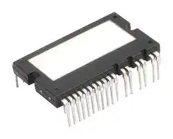
## **ON Semiconductor** ## **Is Now** **==> picture [390 x 69] intentionally omitted <==** **To learn more about onsemi™, please visit our website at www.onsemi.com** **onsemi** and and other names, marks, and brands are registered and/or common law trademarks of Semiconductor Components Industries, LLC dba “ **onsemi** ” or its affiliates and/or subsidiaries in the United States and/or other countries. **onsemi** owns the rights to a number of patents, trademarks, copyrights, trade secrets, and other intellectual property. A listing of **onsemi** product/patent coverage may be accessed at www.onsemi.com/site/pdf/Patent-Marking.pdf. **onsemi** reserves the right to make changes at any time to any products or information herein, without notice. The information herein is provided “as-is” and **onsemi** makes no warranty, representation or guarantee regarding the accuracy of the information, product features, availability, functionality, or suitability of its products for any particular purpose, nor does **onsemi** assume any liability arising out of the application or use of any product or circuit, and specifically disclaims any and all liability, including without limitation special, consequential or incidental damages. Buyer is responsible for its products and applications using **onsemi** products, including compliance with all laws, regulations and safety requirements or standards, regardless of any support or applications information provided by **onsemi** . “Typical” parameters which may be provided in **onsemi** data sheets and/ or specifications can and do vary in different applications and actual performance may vary over time. All operating parameters, including “Typicals” must be validated for each customer application by customer’s technical experts. **onsemi** does not convey any license under any of its intellectual property rights nor the rights of others. **onsemi** products are not designed, intended, or authorized for use as a critical component in life support systems or any FDA Class 3 medical devices or medical devices with a same or similar classification in a foreign jurisdiction or any devices intended for implantation in the human body. Should Buyer purchase or use **onsemi** products for any such unintended or unauthorized application, Buyer shall indemnify and hold **onsemi** and its officers, employees, subsidiaries, affiliates, and distributors harmless against all claims, costs, damages, and expenses, and reasonable attorney fees arising out of, directly or indirectly, any claim of personal injury or death associated with such unintended or unauthorized use, even if such claim alleges that **onsemi** was negligent regarding the design or manufacture of the part. **onsemi** is an Equal Opportunity/Affirmative Action Employer. This literature is subject to all applicable copyright laws and is not for resale in any manner. Other names and brands may be claimed as the property of others. October 2017 ## **FNA41060 / FNA41060B2 Motion SPM[®] 45 Series** ## **Features** - UL Certified No. E209204 (UL1557) - 600 V - 10 A 3-Phase IGBT Inverter with Integral Gate Drivers and Protection - Low Thermal Resistance Using Ceramic Substrate - Low-Loss, Short-Circuit Rated IGBTs - Built-In Bootstrap Diodes and Dedicated Vs Pins Simplify PCB Layout - Built-In NTC Thermistor for Temperature Monitoring - Separate Open-Emitter Pins from Low-Side IGBTs for Three-Phase Current Sensing - Single-Grounded Power Supply ## **General Description** FNA41060 / FNA41060B2 is a Motion SPM[®] 45 module providing a fully-featured, high-performance inverter output stage for AC Induction, BLDC, and PMSM motors. These modules integrate optimized gate drive of the built-in IGBTs to minimize EMI and losses, while also providing multiple on-module protection features including under-voltage lockouts, over-current shutdown, thermal monitoring, and fault reporting. The built-in, highspeed HVIC requires only a sing le supply voltage and translates the incoming logic-level gate inpu ts to the high-voltage, high-current drive signals required to properly drive the module's robust short-circuit-rated IGBTs. Separate negative IGBT terminals are available for each phase to support the widest variety of control algorithms. - Optimized for 5 kHz Switching Frequency - Isolation Rating: 2000 Vrms / min. ## **Applications** - Motion Control - Home Appliance / Industrial Motor ## **Related Resources** - _AN-9070 - Motion SPM® 45 Series Users Guide_ - _AN-9071 - Motion SPM® 45 Series Thermal Performance Information_ - _AN-9072 - Motion SPM® 45 Series Mounting Guidance_ - _RD-344 - Reference Design (Three Shunt Solution)_ - _RD-345 - Reference Design (One Shunt Solution)_ **Figure 1. Package Overview** **Package Marking and Ordering Information Device Device Marking Package Packing Type Quantity** FNA41060 FNA41060 SPMAA-A26 Rail 12 FNA41060B2 FNA41060B2 SPMAA-C26 Rail 12 ~~——_—~~ 1 ©2011 Semiconductor Components Industries, LLC. FNA41060 / FNA41060B2 Rev. 2 www.onsemi.com ## **Integrated Power Functions** - 600 V - 10 A IGBT inverter for three-phase DC / AC power conversion (please refer to Figure 3) ## **Integrated Drive, Protection, and System Control Functions** - For inverter high-side IGBTs: gate drive circuit, high-voltage isolated high-speed level shifting control circuit Under-Voltage Lock-Out (UVLO) protection - For inverter low-side IGBTs: gate drive circuit, Short-Circuit Protection (SCP) control supply circuit Under-Voltage Lock-Out (UVLO) protection - Fault signaling: corresponding to UVLO (low-side supply) and SC faults - Input interface: active-HIGH interface, works with 3.3 / 5 V logic, Schmitt trigger input ## **Pin Configuration** **==> picture [363 x 259] intentionally omitted <==** **----- Start of picture text -----**<br> VB(U)(26)<br>VTH(1) VS(U)(25)<br>RTH(2)<br>VB(V)(24)<br>VS(V)(23)<br>: :<br>P(3)<br>VB(W)(22)<br>VS(W)(21)<br>c i:<br>U(4)<br>Case Temperature (TC) IN(UH)(20)<br>Detecting Point IN(VH)(19)<br>V(5) IN(WH)(18)<br>VCC(H)(17)<br>VCC(L)(16)<br>W(6)<br>COM(15)<br>IN(UL)(14)<br>NU(7) IN(VL)(13)<br>IN(WL)(12)<br>NV(8) VFO(11)<br>NW(9) CSC(10)<br>**----- End of picture text -----**<br> **Figure 2. Top View** 2 ©2011 Semiconductor Components Industries, LLC. www.onsemi.com FNA41060 / FNA41060B2 ## **Pin Descriptions** |**Pin Number**|**Pin Name**|**Pin Description**| |---|---|---| |1|VTH|Thermistor Bias Voltage| |2|RTH|Series Resistor for the Use of Thermistor (Temperature Detection)| |3|P|Positive DC-Link Input| |4|U|Output for U-Phase| |5|V|Output for V-Phase| |6|W|Output for W-Phase| |7|NU|Negative DC-Link Input for U-Phase| |8|NV|Negative DC-Link Input for V-Phase| |9|NW|Negative DC-Link Input for W-Phase| |10|CSC|Capacitor (Low-Pass Filter) for Short-circuit Current Detection Input| |11|VFO|Fault Output| |12|IN(WL)|Signal Input for Low-Side W-Phase| |13|IN(VL)|Signal Input for Low-Side V-Phase| |14|IN(UL)|Signal Input for Low-Side U-Phase| |15|COM|Common Supply Ground| |16|VCC(L)|Low-Side Common Bias Voltage for IC and IGBTs Driving| |17|VCC(H)|High-Side Common Bias Voltage for IC and IGBTs Driving| |18|IN(WH)|Signal Input for High-Side W-Phase| |19|IN(VH)|Signal Input for High-Side V-Phase| |20|IN(UH)|Signal Input for High-Side U-Phase| |21|VS(W)|High-Side Bias Voltage Ground for W-Phase IGBT Driving| |22|VB(W)|High-Side Bias Voltage for W-Phase IGBT Driving| |23|VS(V)|High-Side Bias Voltage Ground for V-Phase IGBT Driving| |24|VB(V)|High-Side Bias Voltage for V-Phase IGBT Driving| |25|VS(U)|High-Side Bias Voltage Ground for U-Phase IGBT Driving| |26|VB(U)|High-Side Bias Voltage for U-Phase IGBT Driving| 3 ©2011 Semiconductor Components Industries, LLC. FNA41060 / FNA41060B2 www.onsemi.com ## **Internal Equivalent Circuit and Input/Output Pins** **==> picture [224 x 333] intentionally omitted <==** **----- Start of picture text -----**<br> VTH (1)<br>Thermister RTH (2)<br>(26) VB(U) UVB P (3)<br>(25) VS(U) UVS<br>OUT(UH)<br>(24) VB(V) VVB UVS U(4)<br>(23) VS(V) VVS<br>(22) VB(W)<br>WVB<br>(21) VS(W) WVS<br>OUT(VH)<br>(20) IN(UH) IN(UH) VVS V (5)<br>(19) IN(VH) IN(VH)<br>(18) IN(WH) IN(WH)<br>(17) VCC(H)<br>VCC OUT(WH)<br>COM WVS W(6)<br>(16) VCC(L) VCC<br>OUT(UL)<br>(15) COM<br>COM<br>NU (7)<br>(14) IN(UL) IN(UL)<br>(13) IN(VL) IN(VL)<br>(12) IN(WL) IN(WL) OUT(VL)<br>(11) VFO NV (8)<br>VFO<br>(10) CSC<br>C(SC)<br>OUT(WL)<br>NW (9)<br>**----- End of picture text -----**<br> ## **Figure 3. Internal Block Diagram** ## **1st Notes:** 1. Inverter high-side is composed of three IGBTs, freewheeling diodes, and one control IC for each IGBT. 2. Inverter low-side is composed of three IGBTs, freewheeling diodes, and one control IC for each IGBT. It has gate drive and protection functions. 3. Inverter power side is composed of four inverter DC-link input terminals and three inverter output terminals. 4 ©2011 Semiconductor Components Industries, LLC. FNA41060 / FNA41060B2 www.onsemi.com **Absolute Maximum Ratings** (TJ = 25°C, unless otherwise specified.) ## **Inverter Part** |**Symbol**|**Parameter**|**Conditions**|**Rating**|**Unit**| |---|---|---|---|---| |VPN|Supply Voltage|Applied between P - NU, NV, NW|450|V| |VPN(Surge)|Supply Voltage (Surge)|Applied between P - NU, NV, NW|500|V| |VCES|Collector - Emitter Voltage||600|V| |± IC|Each IGBT Collector Current|TC= 25°C, TJ <150°C|10|A| |± ICP|Each IGBT Collector Current (Peak)|TC= 25°C, TJ <150°C, Under 1 ms Pulse<br>Width|20|A| |PC|Collector Dissipation|TC= 25°C per Chip|34|W| |TJ|Operating Junction Temperature|(2nd Note 1)|-40 ~ 150|°C| ## **2nd Notes:** 1. The maximum junction temperature rating of the power chips integrated within the Motion SPM[®] 45 product is 150C. ## **Control Part** |**Symbol**|**Parameter**|**Conditions**|**Rating**|**Unit**| |---|---|---|---|---| |VCC|Control Supply Voltage|Applied between VCC(H), VCC(L) - COM|20|V| |VBS|High - Side Control Bias Voltage|Applied between VB(U)- VS(U), VB(V)- VS(V),<br>VB(W)- VS(W)|20|V| |VIN|Input Signal Voltage|Applied between IN(UH), IN(VH), IN(WH),<br>IN(UL), IN(VL), IN(WL)- COM|-0.3 ~ VCC+ 0.3|V| |VFO|Fault Output Supply Voltage|Applied between VFO- COM|-0.3 ~ VCC+ 0.3|V| |IFO|Fault Output Current|Sink Current at VFOpin|1|mA| |VSC|Current-Sensing Input Voltage|Applied between CSC- COM|-0.3 ~ VCC+ 0.3|V| ## **Bootstrap Diode Part** |**Symbol**|**Parameter**||**Conditions**|**Conditions**|**Rating**|**Rating**|**Rating**|**Unit**| |---|---|---|---|---|---|---|---|---| |VRRM|Maximum Repetitive Reverse Voltage||||600|||V| |IF|Forward Current||TC= 25°C, TJ <150°C||0.50|||A| |IFP|Forward Current (Peak)||TC= 25°C, TJ <150°C, Under 1 ms Pulse<br>Width||1.50|||A| |TJ|Operating Junction Temperature||||-40 ~ 150|||°C| |**Total System**||||||||| |**Symbol**|**Parameter**||**Conditions**||**Rating**|||**Unit**| |VPN(PROT)|Self-Protection Supply Voltage Limit<br>(Short-Circuit Protection Capability)||VCC= VBS= 13.5 ~ 16.5 V<br>TJ= 150°C, Non-Repetitive, < 2s||400|||V| |TSTG|Storage Temperature||||-40 ~ 125|||°C| |VISO|Isolation Voltage||60 Hz, Sinusoidal, AC 1 Minute, Connect<br>Pins to Heat Sink Plate||2000|||Vrms| |**Thermal Resistance**||||||||| |**Symbol**|**Parameter**|**Conditions**||**Min.**|**Typ.**|**Max.**|**Unit**|| |Rth(j-c)Q|Junction to Case Thermal Resistance|Inverter IGBT Part (per 1 / 6 module)||-|-|3.6|°C / W|| |Rth(j-c)F||Inverter FWDi Part (per 1 / 6 module)||-|-|4.8|°C / W|| **2nd Notes:** 2. For the measurement point of case temperature (TC), please refer to Figure 2. 5 ©2011 Semiconductor Components Industries, LLC. FNA41060 / FNA41060B2 www.onsemi.com **Electrical Characteristics** (TJ = 25°C, unless otherwise specified.) ## **Inverter Part** |**Inverter Part**|**Inverter Part**|||||||| |---|---|---|---|---|---|---|---|---| |**Symbol**||**Parameter**|**Conditions**||**Min.**|**Typ.**|**Max.**|**Unit**| |VCE(SAT)||Collector - Emitter Saturation<br>Voltage|VCC= VBS= 15 V<br>VIN= 5 V|IC= 10 A, TJ= 25°C|-|1.7|2.2|V| ||VF|FWDi Forward Voltage|VIN= 0 V|IF= 10 A, TJ= 25°C|-|1.8|2.3|V| |HS|tON|Switching Times|VPN= 300 V, VCC= VBS= 15 V, IC= 10 A<br>TJ= 25°C<br>VIN= 0 V5 V, Inductive Load<br>(2nd Note 3)||0.40|0.70|1.20|s| ||tC(ON)||||-|0.20|0.45|s| ||tOFF||||-|0.75|1.25|s| ||tC(OFF)||||-|0.25|0.50|s| ||trr||||-|0.15|-|s| |LS|tON||VPN= 300 V, VCC= VBS= 15 V, IC= 10 A<br>TJ= 25°C<br>VIN= 0 V5 V, Inductive Load<br>(2nd Note 3)||0.40|0.70|1.20|s| ||tC(ON)||||-|0.20|0.45|s| ||tOFF||||-|0.75|1.25|s| ||tC(OFF)||||-|0.25|0.50|s| ||trr||||-|0.15|-|s| ||ICES|Collector - Emitter Leakage<br>Current|VCE= VCES||-|-|1|mA| ## **2nd Notes:** 3. tON and tOFF include the propagation delay of the internal drive IC. tC(ON) and tC(OFF) are the switching time of IGBT itself under the given gate driving condition internally. For the detailed information, please see Figure 4. **==> picture [384 x 260] intentionally omitted <==** **----- Start of picture text -----**<br> 100% IC 100% IC<br>trr<br>V CE IC IC V CE<br>V IN V IN<br>tON tOFF<br>tC(ON) tC(OFF)<br>10% IC<br>V IN(ON) 90% IC 10% V CE V IN(OFF) 10% V CE 10% IC<br>(a) turn-on (b) turn-off<br>**----- End of picture text -----**<br> **Figure 4. Switching Time Definition** 6 ©2011 Semiconductor Components Industries, LLC. FNA41060 / FNA41060B2 www.onsemi.com |**Figure 5. Switching Loss Characteristics (Typical)**<br>**Control Part**<br>0<br>1<br>2<br>3<br>4<br>5<br>6<br>7<br>8<br>9<br>10<br>11<br>0<br>100<br>200<br>300<br>400<br>500<br>600<br>700<br>**Inductive Load, VPN=300V, VCC=15V, TJ=25**℃<br>**IGBT Turn-ON,****_E_**~~**_on_**~~<br>**IGBT Turn-OFF,****_Eoff_**<br>**FRD Turn-OFF,****_E_**~~**_rec_**~~<br>SWITCHING LOSS, ESW[uJ]<br>COLLECTOR CURRENT, Ic[AMPERES]<br>0<br>1<br>2<br>3<br>4<br>5<br>6<br>7<br>8<br>9<br>10<br>11<br>0<br>100<br>200<br>300<br>400<br>500<br>600<br>700<br>**Inductive Load, VPN=300V, VCC=15V, TJ=150**℃<br>**IGBT Turn-ON,****_Eon_**<br>~~**IGBT Turn-OFF,**~~~~**_E_**~~**_off_**<br>**FRD Turn-OFF,****_Erec_**<br>SWITCHING LOSS, ESW[uJ]<br>COLLECTOR CURRENT, Ic[AMPERES]||1<br>2<br>3<br>4<br>5<br>6<br>7<br>8<br>9<br>10<br>11<br>**Inductive Load, VPN=300V, VCC=15V, TJ=25**℃<br>**IGBT Turn-ON,****_E_**~~**_on_**~~<br>**IGBT Turn-OFF,****_Eoff_**<br>**FRD Turn-OFF,****_E_**~~**_rec_**~~<br>COLLECTOR CURRENT, Ic[AMPERES]<br>0<br>100<br>200<br>300<br>400<br>500<br>600<br>700<br>SWITCHING LOSS, ESW[uJ]|1<br>2<br>3<br>4<br>5<br>6<br>7<br>8<br>9<br>10<br>11<br>**Inductive Load, VPN=300V, VCC=15V, TJ=25**℃<br>**IGBT Turn-ON,****_E_**~~**_on_**~~<br>**IGBT Turn-OFF,****_Eoff_**<br>**FRD Turn-OFF,****_E_**~~**_rec_**~~<br>COLLECTOR CURRENT, Ic[AMPERES]<br>0<br>100<br>200<br>300<br>400<br>500<br>600<br>700<br>SWITCHING LOSS, ESW[uJ]|1<br>2<br>3<br>4<br>5<br>6<br>7<br>8<br>9<br>10<br>11<br>**Inductive Load, VPN=300V, VCC=15V, TJ=25**℃<br>**IGBT Turn-ON,****_E_**~~**_on_**~~<br>**IGBT Turn-OFF,****_Eoff_**<br>**FRD Turn-OFF,****_E_**~~**_rec_**~~<br>COLLECTOR CURRENT, Ic[AMPERES]<br>0<br>100<br>200<br>300<br>400<br>500<br>600<br>700<br>SWITCHING LOSS, ESW[uJ]|0<br>1<br>2<br>3<br>4<br>5<br>6<br>7<br>8<br>9<br>10<br>11<br>**Inductive Load, VPN=300V, VCC=15V, TJ=150**℃<br>**IGBT Turn-ON,****_Eon_**<br>~~**IGBT Turn-OFF,**~~~~**_E_**~~**_off_**<br>**FRD Turn-OFF,****_Erec_**<br>COLLECTOR CURRENT, Ic[AMPERES]|0<br>1<br>2<br>3<br>4<br>5<br>6<br>7<br>8<br>9<br>10<br>11<br>**Inductive Load, VPN=300V, VCC=15V, TJ=150**℃<br>**IGBT Turn-ON,****_Eon_**<br>~~**IGBT Turn-OFF,**~~~~**_E_**~~**_off_**<br>**FRD Turn-OFF,****_Erec_**<br>COLLECTOR CURRENT, Ic[AMPERES]|0<br>1<br>2<br>3<br>4<br>5<br>6<br>7<br>8<br>9<br>10<br>11<br>**Inductive Load, VPN=300V, VCC=15V, TJ=150**℃<br>**IGBT Turn-ON,****_Eon_**<br>~~**IGBT Turn-OFF,**~~~~**_E_**~~**_off_**<br>**FRD Turn-OFF,****_Erec_**<br>COLLECTOR CURRENT, Ic[AMPERES]|0<br>1<br>2<br>3<br>4<br>5<br>6<br>7<br>8<br>9<br>10<br>11<br>**Inductive Load, VPN=300V, VCC=15V, TJ=150**℃<br>**IGBT Turn-ON,****_Eon_**<br>~~**IGBT Turn-OFF,**~~~~**_E_**~~**_off_**<br>**FRD Turn-OFF,****_Erec_**<br>COLLECTOR CURRENT, Ic[AMPERES]|0<br>1<br>2<br>3<br>4<br>5<br>6<br>7<br>8<br>9<br>10<br>11<br>**Inductive Load, VPN=300V, VCC=15V, TJ=150**℃<br>**IGBT Turn-ON,****_Eon_**<br>~~**IGBT Turn-OFF,**~~~~**_E_**~~**_off_**<br>**FRD Turn-OFF,****_Erec_**<br>COLLECTOR CURRENT, Ic[AMPERES]|0<br>1<br>2<br>3<br>4<br>5<br>6<br>7<br>8<br>9<br>10<br>11<br>**Inductive Load, VPN=300V, VCC=15V, TJ=150**℃<br>**IGBT Turn-ON,****_Eon_**<br>~~**IGBT Turn-OFF,**~~~~**_E_**~~**_off_**<br>**FRD Turn-OFF,****_Erec_**<br>COLLECTOR CURRENT, Ic[AMPERES]|0<br>1<br>2<br>3<br>4<br>5<br>6<br>7<br>8<br>9<br>10<br>11<br>**Inductive Load, VPN=300V, VCC=15V, TJ=150**℃<br>**IGBT Turn-ON,****_Eon_**<br>~~**IGBT Turn-OFF,**~~~~**_E_**~~**_off_**<br>**FRD Turn-OFF,****_Erec_**<br>COLLECTOR CURRENT, Ic[AMPERES]|0<br>1<br>2<br>3<br>4<br>5<br>6<br>7<br>8<br>9<br>10<br>11<br>**Inductive Load, VPN=300V, VCC=15V, TJ=150**℃<br>**IGBT Turn-ON,****_Eon_**<br>~~**IGBT Turn-OFF,**~~~~**_E_**~~**_off_**<br>**FRD Turn-OFF,****_Erec_**<br>COLLECTOR CURRENT, Ic[AMPERES]| |---|---|---|---|---|---|---|---|---|---|---|---|---| ||||**IGBT Turn-ON,****_E_**~~**_on_**~~<br>**IGBT Turn-OFF,****_Eoff_**<br>**FRD Turn-OFF,****_E_**~~**_rec_**~~||||**IGBT Turn-ON,****_Eon_**<br>~~**IGBT Turn-OFF,**~~~~**_E_**~~**_off_**<br>**FRD Turn-OFF,****_Erec_**|||||| |||||||||||||| |||||||<br>||||||| |||||||<br>||||||| |||||||||||||| |||||||||||||| |||||||||||||| ||0||||0|1||||||| |**Symbol**||**Parameter**||**Conditions**|||||**Min.**|**Typ.**|**Max.**|**Unit**| |IQCCH||Quiescent VCCSupply<br>Current||VCC(H)= 15 V, IN(UH,VH,WH)= 0 V|VCC(H)- COM||||-|-|0.10|mA| |IQCCL||||VCC(L)= 15 V, IN(UL,VL, WL)= 0 V|VCC(L)- COM||||-|-|2.65|mA| |IPCCH||Operating VCCSupply<br>Current||VCC(L)= 15 V, fPWM= 20 kHz, duty<br>= 50%, Applied to One PWM Sig-<br>nal Input for High-Side|VCC(H)- COM||||-|-|0.15|mA| |IPCCL||||VCC(L)= 15 V, fPWM= 20 kHz, duty<br>= 50%, Applied to One PWM Sig-<br>nal Input for Low-Side|VCC(L)- COM||||-|-|3.65|mA| |IQBS||Quiescent VBSSupply<br>Current||VBS= 15 V, IN(UH, VH, WH)= 0 V|VB(U)- VS(U), VB(V)-<br>VS(V), VB(W)- VS(W)||||-|-|0.30|mA| |IPBS||Operating VBSSupply<br>Current||VCC= VBS= 15 V, fPWM= 20 kHz,<br>Duty = 50%, Applied to One PWM<br>Signal Input for High-Side|VB(U)- VS(U), VB(V)-<br>VS(V), VB(W)- VS(W)||||-|-|2.00|mA| |VFOH||Fault Output Voltage||VSC= 0 V, VFOCircuit: 10 kto 5 V Pull-up|||||4.5|-|-|V| |VFOL||||VSC= 1 V, VFOCircuit: 10 kto 5 V Pull-up|||||-|-|0.5|V| |VSC(ref)||Short-Circuit<br>Current Trip Level||VCC= 15 V (2nd Note 4)|||||0.45|0.50|0.55|V| |UVCCD||Supply Circuit<br>Under-Voltage<br>Protection||Detection level|||||10.5|-|13.0|V| |UVCCR||||Reset level|||||11.0|-|13.5|V| |UVBSD||||Detection level|||||10.0|-|12.5|V| |UVBSR||||Reset level|||||10.5|-|13.0|V| |tFOD||Fault-Out Pulse Width|||||||30|-|-|s| |VIN(ON)||ON Threshold Voltage||Applied between IN(UH), IN(VH), IN(WH), IN(UL), IN(VL),<br>IN(WL)- COM|||||-|-|2.6|V| |VIN(OFF)||OFF Threshold Voltage|||||||0.8|-|-|V| |RTH||Resistance of<br>Thermister||@TTH= 25°C, (2nd Note 5)|||||-|47|-|k| |||||@TTH= 100°C|||||-|2.9|-|k| **2nd Notes:** 4. Short-circuit protection is functioning only at the low-sides. 5. TTH is the temperature of thermister itselt. To know case temperature (TC), please make the experiment considering your application. 7 ©2011 Semiconductor Components Industries, LLC. FNA41060 / FNA41060B2 www.onsemi.com **==> picture [382 x 243] intentionally omitted <==** **----- Start of picture text -----**<br> R-T Curve<br>600<br>550<br>R-T Curve in 50 ℃ ~ 125 ℃<br>500 20<br>450 16<br>400<br>12<br>350<br>8<br>300<br>250 4<br>200 0<br>50 60 70 80 90 100 110 120<br>150 Temperature [ ℃ ]<br>100<br>50<br>0<br>-20 -10 0 10 20 30 40 50 60 70 80 90 100 110 120<br>Temperature TTH[ ℃ ]<br>] <br>]<br><br>Resistance[k<br>Resistance[k<br>**----- End of picture text -----**<br> **Figure. 6. R-T Curve of The Built-In Thermistor** **==> picture [469 x 287] intentionally omitted <==** **----- Start of picture text -----**<br> Bootstrap Diode Part<br>Symbol Parameter Conditions Min. Typ. Max. Unit<br>VF Forward Voltage IF = 0.1 A, TC = 25°C - 2.5 - V<br>trr Reverse-Recovery Time IF = 0.1 A, TC = 25°C - 80 - ns<br>Built-In Bootstrap Diode VF-IF Characteristic<br>1.0<br>0.9<br>0.8<br>0.7<br>0.6<br>0.5<br>0.4<br>0.3<br>0.2<br>0.1<br>T =25oC<br>C<br>0.0<br>0 1 2 3 4 5 6 7 8 9 10 11 12 13 14 15<br>VF [V]<br> [A]IF<br>**----- End of picture text -----**<br> **==> picture [230 x 10] intentionally omitted <==** **----- Start of picture text -----**<br> Figure 7. Built-In Bootstrap Diode Characteristic<br>**----- End of picture text -----**<br> - **2nd Notes:** 6. Built-in bootstrap diode includes around 15 Ω resistance characteristic. 8 ©2011 Semiconductor Components Industries, LLC. FNA41060 / FNA41060B2 www.onsemi.com ## **Recommended Operating Conditions** |**Symbol**|**Parameter**|**Conditions**|**Min.**|**Typ.**|**Max.**|**Unit**| |---|---|---|---|---|---|---| |VPN|Supply Voltage|Applied between P - NU, NV, NW|-|300|400|V| |VCC|Control Supply Voltage|Applied between VCC(H), VCC(L)- COM|13.5|15.0|16.5|V| |VBS|High-Side Bias Voltage|Applied between VB(U)- VS(U), VB(V)- VS(V), VB(W)-<br>VS(W)|13.0|15.0|18.5|V| |dVCC/ dt,<br>dVBS/ dt|Control Supply Variation||-1|-|1|V /s| |tdead|Blanking Time for<br>Preventing Arm-Short|For each input signal|1.5|-|-|s| |fPWM|PWM Input Signal|- 40C<TJ <150°C|-|-|20|kHz| |VSEN|Voltage for Current<br>Sensing|Applied between NU, NV, NW- COM<br>(Including Surge-Voltage)|-4||4|V| |PWIN(ON)|Minimun Input Pulse<br>Width|(2nd Note 7)|0.5|-|-|s| |PWIN(OFF)|||0.5|-|-|| **2nd Notes:** 7. This product might not make response if input pulse width is less than the recommanded value. **==> picture [307 x 216] intentionally omitted <==** **----- Start of picture text -----**<br> Allowable Maximum Output Current<br>10<br>9 f =5kHz<br>SW<br>8<br>7<br>6<br>5<br>4<br>3 VDC=300V, VCC=VBS=15V<br>TJ < 150 ℃ , TC ≤ 125 ℃ f =15kHz<br>2 M.I.=0.9, P.F.=0.8 SW<br>Sinusoidal PWM<br>1<br>0<br>0 10 20 30 40 50 60 70 80 90 100 110 120 130 140<br>Case Temperature, TC [ ℃ ]<br>]rms<br> [A<br>IOrms<br>**----- End of picture text -----**<br> ## **Figure 8. Allowable Maximum Output Current** **2nd Notes:** 8. This allowable output current value is the reference data for the safe operation of this product. This may be different from the actual application and operating condition. 9 ©2011 Semiconductor Components Industries, LLC. FNA41060 / FNA41060B2 www.onsemi.com ## **Mechanical Characteristics and Ratings** |**Parameter**|**Conditions**|**Conditions**|**Min.**|**Typ.**|**Max.**|**Unit**| |---|---|---|---|---|---|---| |Device Flatness|See Figure 9||0|-|+ 120|m| |Mounting Torque|Mounting Screw: M3<br>See Figure 10|Recommended 0.7 N • m|0.6|0.7|0.8|N • m| |||Recommended 7.1 kg • cm|6.2|7.1|8.1|kg • cm| |Weight|||-|11.00|-|g| **Figure 9. Flatness Measurement Position** **==> picture [292 x 32] intentionally omitted <==** **----- Start of picture text -----**<br> Pre - Screwing : 1 → 2 i<br>2<br>Final Screwing : 2 → 1<br>**----- End of picture text -----**<br> ## **Figure 10. Mounting Screws Torque Order** ## **2nd Notes:** 9. Do not make over torque when mounting screws. Much mounting torque may cause ceramic cracks, as well as bolts and Al heat-sink destruction. 10. Avoid one side tightening stress. Figure 10 shows the recommended torque order for mounting screws. Uneven mounting can cause the ceramic substrate of the SPM[® ] 45 package to be damaged. The pre-screwing torque is set to 20 ~ 30% of maximum torque rating. 10 ©2011 Semiconductor Components Industries, LLC. FNA41060 / FNA41060B2 www.onsemi.com ## **Time Charts of Protective Function** **==> picture [348 x 198] intentionally omitted <==** **----- Start of picture text -----**<br> Input Signal<br>Protection<br>RESET SET RESET<br>Circuit State<br>UVCCR<br>a1 a6<br>Control UVCCD a3<br>Supply Voltage<br>a2<br>a4 a7<br>Output Current<br>a5<br>Fault Output Signal<br>**----- End of picture text -----**<br> - a1 : Control supply voltage rises: after the voltage rises UVCCR, the circuits start to operate when next input is applied. a2 : Normal operation: IGBT ON and carrying current. - a3 : Under-voltage detection (UVCCD). - a4 : IGBT OFF in spite of control input condition. - a5 : Fault output operation starts. - a6 : Under-voltage reset (UVCCR). a7 : Normal operation: IGBT ON and carrying current. **Figure 11. Under-Voltage Protection (Low-Side)** **==> picture [348 x 188] intentionally omitted <==** **----- Start of picture text -----**<br> Input Signal<br>Protection<br>RESET SET RESET<br>Circuit State<br>UVBSR<br>b1 b5<br>Control UVBSD b3<br>Supply Voltage b6<br>b2<br>b4<br>Output Current<br>High-level (no fault output)<br>Fault Output Signal<br>**----- End of picture text -----**<br> - b1 : Control supply voltage rises: after the voltage reaches UVBSR, the circuits start to operate when next input is applied. b2 : Normal operation: IGBT ON and carrying current. - b3 : Under-voltage detection (UVBSD). - b4 : IGBT OFF in spite of control input condition, but there is no fault output signal. - b5 : Under-voltage reset (UVBSR). - b6 : Normal operation: IGBT ON and carrying current. ## **Figure 12. Under-Voltage Protection (High-Side)** 11 ©2011 Semiconductor Components Industries, LLC. FNA41060 / FNA41060B2 www.onsemi.com **==> picture [307 x 251] intentionally omitted <==** **----- Start of picture text -----**<br> Lower Arms<br>c6 c7<br>Control Input<br>Protection<br>Circuit State SET RESET<br>Internal IGBT c4<br>Gate - Emitter Voltage c3<br>c2<br>SC<br>c1<br>Output Current c8<br>SC Reference Voltage<br>Sensing Voltage<br>of Shunt Resistance<br>CR Circuit Time<br>Fault Output Signal c5 Constant Delay<br>**----- End of picture text -----**<br> (with the external shunt resistance and CR connection) c1 : Normal operation: IGBT ON and carrying current. c2 : Short-circuit current detection (SC trigger). c3 : Hard IGBT gate interrupt. c4 : IGBT turns OFF. c5 : Input “LOW”: IGBT OFF state. c6 : Input “HIGH”: IGBT ON state, but during the active period of fault output, the IGBT doesn’t turn ON. c7 : IGBT OFF state. ## **Figure 13. Short-Circuit Protection (Low-Side Operation Only)** ## **Input/Output Interface Circuit** +5 V (for MCU or Control power) **==> picture [469 x 175] intentionally omitted <==** **----- Start of picture text -----**<br> RPF = 10 kΩ SPM<br>IN(UH) , IN (VH) , IN(WH)<br>IN (UL) , IN (VL) , IN(WL)<br>MCU<br>VFO<br>COM<br>Figure 14. Recommended MCU I/O Interface Circuit<br>2nd Notes:<br>11. RC coupling at each input (parts shown dotted) might change depending on the PWM control scheme in the application and the wiring impedance of the application’s printed<br>circuit board. The input signal section of the Motion SPM [®] 45 product integrates a 5 k ( typ.) pull-down resistor. Therefore, when using an external filtering resistor, pay atten-<br>tion to the signal voltage drop at input terminal.<br>**----- End of picture text -----**<br> 12 ©2011 Semiconductor Components Industries, LLC. FNA41060 / FNA41060B2 www.onsemi.com **==> picture [469 x 514] intentionally omitted <==** **----- Start of picture text -----**<br> HVIC<br>(26) VB(U) VB(U) P (3)<br>CBS CBSC (25) VS(U) VS(U)<br>Gating UH RS (20) IN(UH) IN(UH) OUT(UH)VS( U) U (4)<br>_ os ese<br>(24) VB(V) VB(V)<br>Gating VH RS CBS CBSC (19) IN(23) VS(V)(VH) IN(VH)VS(V) OUT(VH)<br>a l (22) VB(W) VB(W) VS( V) TS V (5) M<br>CBS CBSC (21) VS(W) VS(W)<br>M Gating WH RS +15 V (18) IN(17) VCC(H)(WH) IN(WH)VCC OUT(WH) CDCS VDC<br>C CPS CPS CPS CSP15 CSPC15 (15) COM COM VS( W) W (6)<br>U +5 V LVIC<br>(16) VCC(L) VCC<br>OUT(UL)<br>RS RPF CSPC05 CSP05 (11) VFO NU (7) RSU<br>Fault VFO<br>Gating WLGating ULGating VL CBPF CPF RRRSSS CSC (14) IN(13) IN(12) IN(UL)(VL)(WL) IN(UL)IN(VL)IN(WL)COM OUT(WL)OUT(VL) NV (8) RSV<br>CPS CPS CPS RF (10) CSC CSC NW (9) RSW<br>(1) VTH<br>RTH (2) RTH THERMISTOR<br>U-Phase Current<br>Input Signal for<br>V-Phase Current<br>Short-Circuit Protection<br>| Temp. Monitoring W-Phase Current<br>Figure 15. Typical Application Circuit<br>3rd Notes:<br>1) To avoid malfunction, the wiring of each input should be as short as possible (less than 2 - 3 cm).<br>2) By virtue of integrating an application-specific type of HVIC inside the Motion SPM [[®]] 45 product, direct coupling to MCU terminals without any optocoupler or transformer isola-<br>tion is possible.<br>3) VFO output is open-drain type. This signal line should be pulled up to the positive side of the MCU or control power supply with a resistor that makes IFO up to 1 mA (pleaseFO output is open-drain type. This signal line should be pulled up to the positive side of the MCU or control power supply with a resistor that makes IFO up to 1 mA (please output is open-drain type. This signal line should be pulled up to the positive side of the MCU or control power supply with a resistor that makes IFO up to 1 mA (pleaseFO up to 1 mA (please up to 1 mA (please<br>refer to Figure 14).<br>4) CSP15 of around seven times larger than bootstrap capacitor CBS is recommended.<br>5) Input signal is active-HIGH type. There is a 5 k resistor inside the IC to pull down each input signal line to GND. RC coupling circuits is recommanded for the prevention of<br>input signal oscillation. RSCPS time constant should be selected in the range 50 ~ 150 ns (recommended RS = 100 Ω , CPS = 1 nF).<br>6) To prevent errors of the protection function, the wiring around RF and CSC should be as short as possible.<br>7) In the short-circuit protection circuit, please select the RFCSC time constant in the range 1.5 ~ 2 s.FCSC time constant in the range 1.5 ~ 2 s.CSC time constant in the range 1.5 ~ 2 s.SC time constant in the range 1.5 ~ 2 s. time constant in the range 1.5 ~ 2 s.s.s.<br>8) The connection between control GND line and power GND line which includes the NU, NV, NW must be connected to only one point. Please do not connect the control GNDU, NV, NW must be connected to only one point. Please do not connect the control GND, NV, NW must be connected to only one point. Please do not connect the control GNDV, NW must be connected to only one point. Please do not connect the control GND, NW must be connected to only one point. Please do not connect the control GNDW must be connected to only one point. Please do not connect the control GND must be connected to only one point. Please do not connect the control GND<br>to the power GND by the broad pattern. Also, the wiring distance between control GND and power GND should be as short as possible.<br>9) Each capacitor should be mounted as close to the pins of the Motion SPM 45 product as possible.<br>10) To prevent surge destruction, the wiring between the smoothing capacitor and the P & GND pins should be as short as possible. The use of a high-frequency non-inductive<br>capacitor of around 0.1 ~ 0.22 F between the P and GND pins is recommended.<br>**----- End of picture text -----**<br> **3rd Notes:** - 1) To avoid malfunction, the wiring of each input should be as short as possible (less than 2 - 3 cm). - 2) By virtue of integrating an application-specific type of HVIC inside the Motion SPM[[®]] 45 product, direct coupling to MCU terminals without any optocoupler or transformer isolation is possible. - 3) VFO output is open-drain type. This signal line should be pulled up to the positive side of the MCU or control power supply with a resistor that makes IFO up to 1 mA (pleaseFO output is open-drain type. This signal line should be pulled up to the positive side of the MCU or control power supply with a resistor that makes IFO up to 1 mA (please output is open-drain type. This signal line should be pulled up to the positive side of the MCU or control power supply with a resistor that makes IFO up to 1 mA (pleaseFO up to 1 mA (please up to 1 mA (please refer to Figure 14). - 7) In the short-circuit protection circuit, please select the RFCSC time constant in the range 1.5 ~ 2 s.FCSC time constant in the range 1.5 ~ 2 s.CSC time constant in the range 1.5 ~ 2 s.SC time constant in the range 1.5 ~ 2 s. time constant in the range 1.5 ~ 2 s.s.s. 8) The connection between control GND line and power GND line which includes the NU, NV, NW must be connected to only one point. Please do not connect the control GNDU, NV, NW must be connected to only one point. Please do not connect the control GND, NV, NW must be connected to only one point. Please do not connect the control GNDV, NW must be connected to only one point. Please do not connect the control GND, NW must be connected to only one point. Please do not connect the control GNDW must be connected to only one point. Please do not connect the control GND must be connected to only one point. Please do not connect the control GND to the power GND by the broad pattern. Also, the wiring distance between control GND and power GND should be as short as possible. - 11) Relays are used in almost every systems of electrical equipment in home appliances. In these cases, there should be sufficient distance between the MCU and the relays. - 12) The zener diode or transient voltage suppressor should be adopted for the protection of ICs from the surge destruction between each pair of control supply terminals (recommanded zener diode is 22 V / 1 W, which has the lower zener impedance characteristic than about 15 Ω ). - 13) Please choose the electrolytic capacitor with good temperature characteristic in CBS. Also, choose 0.1 ~ 0.2 F R-category ceramic capacitors with good temperature and frequency characteristics in CBSC. - 14) For the detailed information, please refer to the AN-9070, AN-9071, AN-9072, RD-344, and RD-345. 13 ©2011 Semiconductor Components Industries, LLC. FNA41060 / FNA41060B2 www.onsemi.com ## **Package Outline Drawing (FNA41060)** **SPMAA−A26 / 26LD, PDD STD, CERAMIC TYPE, STANDARD DUAL FORM** CASE MODFA ISSUE O ## **Package Outline Drawing (FNA41060B2, Long Terminal Type)** ## **SPMAA−C26 / 26LD, PDD STD CERAMIC TYPE, LONG LEAD DUAL FORM TYPE** CASE MODFC ISSUE O ON Semiconductor and are trademarks of Semiconductor Components Industries, LLC dba ON Semiconductor or its subsidiaries in the United States and/or other countries. ON Semiconductor owns the rights to a number of patents, trademarks, copyrights, trade secrets, and other intellectual property. A listing of ON Semiconductor’s product/patent coverage may be accessed at www.onsemi.com/site/pdf/Patent−Marking.pdf. ON Semiconductor reserves the right to make changes without further notice to any products herein. ON Semiconductor makes no warranty, representation or guarantee regarding the suitability of its products for any particular purpose, nor does ON Semiconductor assume any liability arising out of the application or use of any product or circuit, and specifically disclaims any and all liability, including without limitation special, consequential or incidental damages. Buyer is responsible for its products and applications using ON Semiconductor products, including compliance with all laws, regulations and safety requirements or standards, regardless of any support or applications information provided by ON Semiconductor. “Typical” parameters which may be provided in ON Semiconductor data sheets and/or specifications can and do vary in different applications and actual performance may vary over time. All operating parameters, including “Typicals” must be validated for each customer application by customer’s technical experts. ON Semiconductor does not convey any license under its patent rights nor the rights of others. ON Semiconductor products are not designed, intended, or authorized for use as a critical component in life support systems or any FDA Class 3 medical devices or medical devices with a same or similar classification in a foreign jurisdiction or any devices intended for implantation in the human body. Should Buyer purchase or use ON Semiconductor products for any such unintended or unauthorized application, Buyer shall indemnify and hold ON Semiconductor and its officers, employees, subsidiaries, affiliates, and distributors harmless against all claims, costs, damages, and expenses, and reasonable attorney fees arising out of, directly or indirectly, any claim of personal injury or death associated with such unintended or unauthorized use, even if such claim alleges that ON Semiconductor was negligent regarding the design or manufacture of the part. ON Semiconductor is an Equal Opportunity/Affirmative Action Employer. This literature is subject to all applicable copyright laws and is not for resale in any manner. ## **PUBLICATION ORDERING INFORMATION** **LITERATURE FULFILLMENT** : **N. American Technical Support** : 800−282−9855 Toll Free **ON Semiconductor Website** : **www.onsemi.com** Literature Distribution Center for ON Semiconductor USA/Canada 19521 E. 32nd Pkwy, Aurora, Colorado 80011 USA **Europe, Middle East and Africa Technical Support: Order Literature** : http://www.onsemi.com/orderlit **Phone** : 303−675−2175 or 800−344−3860 Toll Free USA/Canada Phone: 421 33 790 2910 **Fax** : 303−675−2176 or 800−344−3867 Toll Free USA/Canada **Japan Customer Focus Center** For additional information, please contact your local **Email** : orderlit@onsemi.com Phone: 81−3−5817−1050 Sales Representative **www.onsemi.com** **1**
Updated at April 27, 2026
onsemi is a premier global supplier of intelligent power and sensing technologies, driving disruptive innovations across the automotive, industrial, and cloud infrastructure markets. Recognized for their commitment to sustainability and reliable supply chains, the company accelerates advancements in vehicle electrification, industrial automation, and 5G networks by solving the industry's most complex design challenges. At the core of their portfolio is an industry-leading selection of discrete semiconductors. This extensive range features thousands of high-performance bipolar transistors, single and dual MOSFETs, and a comprehensive array of diodes, including Zener, Schottky, and fast-recovery rectifiers. Engineered for superior thermal performance and energy efficiency, these foundational components are critical for demanding power conversion, switching, and signal conditioning applications. Beyond essential discretes, onsemi provides a robust suite of advanced power management and circuit protection solutions. Their lineup includes intelligent power modules, single IGBTs, and transient voltage suppression (TVS) diodes designed to safeguard sensitive circuitry. Complimented by integrated passive filters, AC/DC LED driver ICs, and specialized sub-2.4GHz RF transceivers, onsemi equips engineers with the scalable, high-quality technologies needed to build a cleaner, smarter, and more connected world.
About Novapart
Novapart is a B2B electronic component broker specialising in stock shortages and cost reduction. We source hard-to-find parts and identify compliant alternatives across a catalogue of 420,000+ components from 500+ manufacturers.
Learn more →Stock Shortage Specialist
When a component is unavailable, discontinued or has an unacceptable lead time, we tap into our network of vetted European and Asian distributors to source what you need — without compromising on quality or traceability.
Request a quote →Compliant Alternatives
We identify pin-to-pin, electrically equivalent substitutes that meet the same certifications (RoHS, AEC-Q100, REACH) as your original specification — validated against datasheets, not just part numbers. Often at a lower cost.
BOM Analysis service →