


FDPC8011S
Dual MOSFET, N Channel, 25 V, 25 V, 60 A, 60 A, 0.006 ohm
- Manufacturer: ONSEMI
- Product type: Dual MOSFETs
- Transistor Polarity:Dual N Channel; Continuous Drain Current Id:60A; Drain Source Voltage Vds:25V; On Resistance Rds(on):0.0012ohm; Rds(on) Test Voltage Vgs:10V; Threshold Voltage Vgs:
- MSL: MSL 1 - Unlimited
- SVHC: Lead (25-Jun-2025)
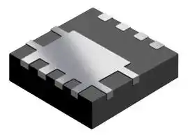
- No. of Pins: 8Pins
- Channel Type: N Channel
- Product Range: -
- Qualification: -
- Transistor Case Style: Power 33
- Operating Temperature Max: 150°C
- Power Dissipation N Channel: 2W
- Power Dissipation P Channel: 2W
- Drain Source Voltage Vds N Channel: 25V
- Drain Source Voltage Vds P Channel: 25V
- Continuous Drain Current Id N Channel: 60A
- Continuous Drain Current Id P Channel: 60A
- Drain Source On State Resistance N Channel: 0.006ohm
- Drain Source On State Resistance P Channel: -
| Delivery and price | |
|---|---|
| Units per pack | 5000 |
| Price | 0.551 € |
| Current stock | 10+ |
| Lead time | 30 days |
## **Is Now Part of**

## **To learn more about ON Semiconductor, please visit our website at www.onsemi.com**

Please note: As part of the Fairchild Semiconductor integration, some of the Fairchild orderable part numbers will need to change in order to meet ON Semiconductor’s system requirements. Since the ON Semiconductor product management systems do not have the ability to manage part nomenclature that utilizes an underscore (_), the underscore (_) in the Fairchild part numbers will be changed to a dash (-). This document may contain device numbers with an underscore (_). Please check the ON Semiconductor website to verify the updated device numbers. The most current and up-to-date ordering information can be found at www.onsemi.com. Please email any questions regarding the system integration to Fairchild_questions@onsemi.com.

ON Semiconductor and the ON Semiconductor logo are trademarks of Semiconductor Components Industries, LLC dba ON Semiconductor or its subsidiaries in the United States and/or other countries. ON Semiconductor owns the rights to a number of patents, trademarks, copyrights, trade secrets, and other intellectual property. A listing of ON Semiconductor’s product/patent coverage may be accessed at www.onsemi.com/site/pdf/Patent-Marking.pdf. ON Semiconductor reserves the right to make changes without further notice to any products herein. ON Semiconductor makes no warranty, representation or guarantee regarding the suitability of its products for any particular purpose, nor does ON Semiconductor assume any liability arising out of the application or use of any product or circuit, and specifically disclaims any and all liability, including without limitation special, consequential or incidental damages. Buyer is responsible for its products and applications using ON Semiconductor products, including compliance with all laws, regulations and safety requirements or standards, regardless of any support or applications information provided by ON Semiconductor. “Typical” parameters which may be provided in ON Semiconductor data sheets and/or specifications can and do vary in different applications and actual performance may vary over time. All operating parameters, including “Typicals” must be validated for each customer application by customer’s technical experts. ON Semiconductor does not convey any license under its patent rights nor the rights of others. ON Semiconductor products are not designed, intended, or authorized for use as a critical component in life support systems or any FDA Class 3 medical devices or medical devices with a same or similar classification in a foreign jurisdiction or any devices intended for implantation in the human body. Should Buyer purchase or use ON Semiconductor products for any such unintended or unauthorized application, Buyer shall indemnify and hold ON Semiconductor and its officers, employees, subsidiaries, affiliates, and distributors harmless against all claims, costs, damages, and expenses, and reasonable attorney fees arising out of, directly or indirectly, any claim of personal injury or death associated with such unintended or unauthorized use, even if such claim alleges that ON Semiconductor was negligent regarding the design or manufacture of the part. ON Semiconductor is an Equal Opportunity/Affirmative Action Employer. This literature is subject to all applicable copyright laws and is not for resale in any manner.

**==> picture [64 x 9] intentionally omitted <==**

**----- Start of picture text -----**<br>
October 2014<br>**----- End of picture text -----**<br>


## **FDPC8011S**

## **PowerTrench[®] Power Clip 25V Asymmetric Dual N-Channel MOSFET**

## **Features**

Q1: N-Channel

Max rDS(on) = 7.3 mΩ at VGS = 4.5 V, ID = 12 A

Q2: N-Channel

Max rDS(on) = 2.1 mΩ at VGS = 4.5 V, ID =  24 A

Low inductance packaging shortens rise/fall times, resulting in lower switching losses

MOSFET integration enables optimum layout for lower circuit inductance and reduced switch node ringing

RoHS Compliant

## **General Description**

This device includes two specialized N-Channel MOSFETs in a dual package. The switch node has been internally connected to enable easy placement and routing of synchronous buck converters. The control MOSFET (Q1) and synchronous SyncFET[TM] (Q2) have been designed to provide optimal power efficiency.

## **Applications**

Computing

Communications

General Purpose Point of Load

|**Pin 1**|||||||||||||||||
|---|---|---|---|---|---|---|---|---|---|---|---|---|---|---|---|---|
||**GND**<br>**(LSS**<br>**HSG**<br>**Pin 1**<br>**V+**<br>**(HSD**<br>**V+**<br>**LS**<br>**GND**<br>**GND**|**Pin 1**<br>**HSG**<br>**SW**<br>-|||1|**PAD9**<br>**V+(HSD)**<br> bed|ro|**V+**<br>**LSG**||**HSG**<br>**SW**|——|||r=||**V+**<br>**LSG**|
||**SW**<br>**SW**<br>**SW**|**SW**|a <br>31||**PAD10**<br> fe<br>|<br>i 16<br>7|||**GND**||**SW**|-<br>3}|**SW**||-<br>16||**GND**|
|**Top**|**Bottom**<br>**3.3 mm x 3.3 mm**|**SW**|1<br>ai!<br>a|||**GND(LSS)**<br>'<br>1|Ts<br>“=|**GND**||**SW**|.<br>4|Q2||.<br>15||**GND**|
|**MOSFET Maximum Ratings  **TA= 25 °C unless otherwise noted|||||||||||||||||
|**Symbol**|**Parameter**|||||||||**Q1**|||**Q2**||**Units**||
|VDS|Drain to Source Voltage|||||||||25|||25|||V|
|VGS|Gate to Source Voltage|e|e|e|e|e|e|||12|||12|||V|
||Drain Current      -Continuous(Package limited)T|T|T|T|T|TC = 25 °C|= 25 °C|||20|||60||||
|ID|-Continuous                                                                    T|-Continuous                                                                    T|-Continuous                                                                    T|-Continuous                                                                    T|-Continuous                                                                    T|-Continuous                                                                    TA= 25 °C|= 25 °C|||131a||271b||||A|
||-Pulsed|||||||||40||120||120|||
|EAS|Single Pulse Avalanche Energy|||||(Note 3)||||21|||97|||mJ|
|PD|Power Dissipation for Single Operation                                                  T<br>Power Dissipation for Single Operation                                                  T|eration                                                  T<br>eration                                                  T|eration                                                  T<br>eration                                                  T|eration                                                  T<br>eration                                                  T|eration                                                  T<br>eration                                                  T|eration                                                  TA= 25 °C<br>eration                                                  TA= 25 °C|= 25 °C<br>= 25 °C|||1.61a<br>0.81c||2.01b<br>0.91d||||W|
|TJ, TSTG|Operatingand Storage Junction Temperature Range|||||||||-55 to +150||-55 to +150||||°C|
|**Thermal Characteristics**|||||||||||||||||
|RθJA|Thermal Resistance, Junction to Ambient|Thermal Resistance, Junction to Ambient|Thermal Resistance, Junction to Ambient|Thermal Resistance, Junction to Ambient|Thermal Resistance, Junction to Ambient|Thermal Resistance, Junction to Ambient||||771a||631b|||||
|RθJA|Thermal Resistance, Junction to Ambient|Thermal Resistance, Junction to Ambient|Thermal Resistance, Junction to Ambient|Thermal Resistance, Junction to Ambient|Thermal Resistance, Junction to Ambient|Thermal Resistance, Junction to Ambient||||1511c||1351d||||°C/W|
|RθJC|Thermal Resistance, Junction to Case|Thermal Resistance, Junction to Case|Thermal Resistance, Junction to Case|Thermal Resistance, Junction to Case|Thermal Resistance, Junction to Case|Thermal Resistance, Junction to Case||||5.0||3.5|||||
|**Package Marking and Ordering Information**|||||||||||||||||
|**Device Marking**<br>**Device**<br>**Package**||||||**Reel Size**|||**Tape Width**|||||**Quantity**|||
|13OD/15OD<br>FDPC8011S<br>Power Clip33||||||13 ”||||12 mm||||3000 units|||


**1**

©2012 Fairchild Semiconductor Corporation FDPC8011S Rev.C6

www.fairchildsemi.com

|**Electrical Characteristics**TJ= 25 °C unless otherwise noted|**Electrical Characteristics**TJ= 25 °C unless otherwise noted|**Electrical Characteristics**TJ= 25 °C unless otherwise noted||||||||
|---|---|---|---|---|---|---|---|---|---|
|**Symbol**|**Parameter**|**Test Conditions**|**Type**|**Min**||**Typ**|**Max**||**Units**|
|**Off Characteristics**||||||||||
|BVDSS|Drain to Source Breakdown Voltage|ID= 250μA, VGS= 0 V<br>ID= 1 mA, VGS= 0 V|Q1<br>Q2|25<br>25|||||V|
|ΔBVDSS<br>ΔTJ|Breakdown Voltage Temperature<br>Coefficient|ID= 250μA, referenced to 25 °C<br>ID= 10 mA, referenced to 25 °C|Q1<br>Q2|||14<br>24|||mV/°C|
|IDSS|Zero Gate Voltage Drain Current|VDS= 20 V, VGS= 0 V<br>VDS= 20 V, VGS = 0 V|Q1<br>Q2||||1<br>500||μA<br>μA|
|IGSS|Gate to Source Leakage Current,<br>Forward|VGS= 12 V/-8 V, VDS= 0 V<br>VGS= 12 V/-8 V, VDS= 0 V|Q1<br>Q2||||±100<br>±100||nA<br>nA|
|**On Characteristics**||||||||||
|VGS(th)|Gate to Source Threshold Voltage|VGS= VDS,  ID= 250μA<br>VGS= VDS,  ID= 1 mA|Q1<br>Q2|0.8<br>1.1||1.2<br>1.4|2.2<br>2.2||V|
|ΔVGS(th)<br>ΔTJ|Gate to Source Threshold Voltage<br>Temperature Coefficient|ID= 250μA, referenced to 25 °C<br>ID= 10 mA, referenced to 25 °C|Q1<br>Q2|||-4<br>-3|||mV/°C|
|rDS(on)|Drain to Source On Resistance|VGS= 10 V,  ID= 13 A<br>VGS= 4.5 V,  ID= 12 A<br>VGS= 10 V, ID= 13 A,TJ=125 °C|Q1|||4.6<br>5.4<br>5.6|6.0<br>7.3<br>7.3||mΩ|
|||VGS= 10 V,  ID=  27 A<br>VGS= 4.5 V,  ID= 24  A<br>VGS= 10 V, ID= 27 A ,TJ=125 °C|Q2|||1.2<br>1.4<br>1.7|1.8<br>2.1<br>2.4|||
|gFS|Forward Transconductance|VDS= 5 V,  ID=  13 A<br>VDS= 5 V,  ID=  27 A|Q1<br>Q2|||97<br>231|||S|
|**Dynamic Characteristics**||||||||||
|Ciss|Input Capacitance|Q1:<br>VDS= 13 V, VGS= 0 V, f = 1 MHZ<br>Q2:<br>VDS= 13 V, VGS= 0 V, f = 1 MHZ|Q1<br>Q2|||1240<br>4335|||pF|
|Coss|Output Capacitance||Q1<br>Q2|||332<br>1126|||pF|
|Crss|Reverse Transfer Capacitance||Q1<br>Q2|||49<br>143|||pF|
|Rg|Gate Resistance||Q1<br>Q2|||0.4<br>0.5|||Ω|
|**Switching Characteristics**||||||||||
|td(on)|Turn-On Delay Time|Q1:<br>VDD= 13 V, ID= 13 A, RGEN= 6Ω<br>Q2:<br>VDD= 13 V, ID= 27 A, RGEN= 6Ω|Q1<br>Q2|||7<br>13|||ns|
|tr|Rise Time||Q1<br>Q2|||2<br>5|||ns|
|td(off)|Turn-Off Delay Time||Q1<br>Q2|||20<br>38|||ns|
|tf|Fall Time||Q1<br>Q2|||2<br>4|||ns|
|Qg|Total Gate Charge|VGS= 0  V to 10 V|Q1<br>Q2|||19<br>64|||nC|
|Qg|Total Gate Charge|VGS= 0  V to 4.5 V|Q1<br>Q2|||9<br>30|||nC|
|Qgs|Gate to Source Gate Charge||Q1<br>Q2|||2.6<br>9.3|||nC|
|Qgd|Gate to Drain “Miller” Charge||Q1<br>Q2|||2.3<br>7.7|||nC|


©2012 Fairchild Semiconductor Corporation FDPC8011S Rev.C6

www.fairchildsemi.com

**2**

**Electrical Characteristics** TJ = 25 °C unless otherwise noted **Symbol Parameter Test Conditions Type Min Typ Max Units** ~~aa~~ **Drain-Source Diode Characteristics** Q1 0.8 1.2 VSD Source to Drain Diode Forward Voltage[V] V[GS ] GS[= 0 V, I] = 0 V, I[S ] S[= 13 A           (Note 2)] =  27 A          (Note 2) Q2 0.8 1.2 V Q1 Q1 22 trr Reverse Recovery Time IF = 13 A, di/dt = 100 A/μs Q2 30 ns Q2 Q1 8 Qrr Reverse Recovery Charge IF = 27 A, di/dt = 300 A/μs Q2 32 nC ~~a~~ Notes: 1.RθJA is determined with the device mounted on a 1 in[2] pad 2 oz copper pad on a 1.5 x 1.5 in. board of FR-4 material. RθJC is guaranteed by design while RθCA is determined by the user's board design.

**==> picture [373 x 217] intentionally omitted <==**

**----- Start of picture text -----**<br>
a. 77 °C/W when mounted on   b. 63 °C/W when mounted on<br>    a 1 in [2 ] pad of  2 oz  copper     a 1 in [2 ] pad of  2 oz  copper<br>$3838 $3838<br>c. 151 °C/W when mounted on  a d. 135 °C/W when mounted on  a<br>    minimum pad of 2 oz copper     minimum pad of 2 oz copper<br>5 A<br>00000 ooooo0<br>DF DS SF SS G DF DS SF SS<br>G DF DS SF SS G DF DS SF SS<br>**----- End of picture text -----**<br>


- 2 Pulse Test: Pulse Width < 300 μs, Duty cycle < 2.0%.

3. Q1 :EAS of 21 mJ is based on starting TJ = 25[o] C; N-ch: L = 1.2 mH, IAS = 6 A, VDD = 23 V, VGS = 10 V. 100% test at L= 0.1 mH, IAS = 14.5 A. Q2: EAS of 97 mJ is based on starting TJ = 25[o] C; N-ch: L = 0.6 mH, IAS = 18 A, VDD = 23 V, VGS = 10 V. 100% test at L= 0.1 mH, IAS = 32.9 A.

©2012 Fairchild Semiconductor Corporation FDPC8011S Rev.C6

www.fairchildsemi.com

**3**

## **Typical Characteristics (Q1 N-Channel)** TJ = 25 °C unless otherwise noted

**==> picture [469 x 576] intentionally omitted <==**

**----- Start of picture text -----**<br>
40 4.0<br>VGS = 10 V VGS = 2.5 V PULSE DURATION = 80  μ s<br>VGS = 4.5 V 3.5 DUTY CYCLE = 0.5% MAX<br>30 V GS = 3.5 V 3.0<br>VGS = 3 V<br>2.5<br>20 VGS = 2.5 V VGS = 3 V<br>2.0<br>VGS = 3.5 V<br>1.5<br>10<br>1.0<br>PULSE DURATION = 80 DUTY CYCLE = 0.5% MAX μ s VGS = 4.5 V VGS = 10 V<br>0 0.5<br>0.0 0.3 0.6 0.9 1.2 1.5 0 10 20 30 40<br>ID, DRAIN CURRENT (A)<br>VDS, DRAIN TO SOURCE VOLTAGE (V)<br>Figure 1.  On Region Characteristics Figure 2.      Normalized On-Resistance<br>vs Drain Current and Gate Voltage<br>1.6 20<br>IVDGS = 13 A = 10 V ID = 13 A PULSE DURATION = 80 DUTY CYCLE = 0.5% MAX μ s<br>1.4 16<br>1.2 12<br>1.0 8 TJ = 125 [ o] C<br>0.8 4<br>TJ = 25  [o] C<br>0.6 0<br>-75 -50 -25 0 25 50 75 100 125 150 2 3 4 5 6 7 8 9 10<br>TJ, JUNCTION TEMPERATURE ( [o] C) VGS, GATE TO SOURCE VOLTAGE (V)<br>Figure 3.  Normalized  On  Resistance                                         Figure 4.   On-Resistance vs  Gate to<br>vs Junction Temperature Source Voltage<br>40 40<br>PULSE DURATION = 80  μ s V GS  = 0 V<br>DUTY CYCLE = 0.5% MAX<br>10<br>30 VDS = 5 V<br>20 1 TJ = 150  [o] C TJ = 25 [ o] C<br>TJ = 150  [o] C TJ = 25  [o] C<br>0.1<br>10 TJ = -55  [o] C<br>TJ = -55  [o] C<br>0 0.01<br>1.0 1.5 2.0 2.5 3.0 0.0 0.2 0.4 0.6 0.8 1.0 1.2<br>VGS, GATE TO SOURCE VOLTAGE (V) VSD, BODY DIODE FORWARD VOLTAGE (V)<br>Figure 5.  Transfer Characteristics Figure 6.    Source to Drain  Diode<br>Forward Voltage vs Source Current<br>NORMALIZED<br>, DRAIN CURRENT (A)<br>ID<br>DRAIN TO SOURCE ON-RESISTANCE<br>) Ω<br>(m<br>DRAIN TO<br>NORMALIZED rDS(on),<br>SOURCE ON-RESISTANCE<br> DRAIN TO SOURCE ON-RESISTANCE<br>, DRAIN CURRENT (A)<br>ID<br>, REVERSE DRAIN CURRENT (A)<br>IS<br>**----- End of picture text -----**<br>


©2012 Fairchild Semiconductor Corporation FDPC8011S Rev.C6

www.fairchildsemi.com

**4**

## **Typical Characteristics (Q1 N-Channel)** TJ = 25 °C unless otherwise noted

**==> picture [472 x 575] intentionally omitted <==**

**----- Start of picture text -----**<br>
10 2000<br>ID = 13 A<br>1000<br>Ciss<br>8<br>6<br>C oss<br>VDD = 10 V VDD = 15 V 100<br>4<br>VDD = 13 V<br>2 C rss<br>f = 1 MHz<br>VGS = 0 V<br>0 10<br>0 4 8 12 16 20 0.1 1 10 30<br>Qg, GATE CHARGE (nC) VDS, DRAIN TO SOURCE VOLTAGE (V)<br>Figure 7.  Gate Charge Characteristics Figure 8.      Capacitance vs Drain<br>to Source Voltage<br>50 60<br>50 VGS = 10 V<br>TJ = 25 [ o] C 40<br>10<br>30<br>T J  = 100 [ o] C VGS = 4.5 V<br>TJ = 125  [o] C 20<br>10 Limited by Package<br>R θ JC = 5.0  [o] C/W<br>1 0<br>0.001 0.01 0.1 1 10 50 25 50 75 100 125 150<br>tAV, TIME IN AVALANCHE (ms) TC, CASE TEMPERATURE (oC)<br>Figure 9.  Unclamped Inductive                                          Figure 10.  Maximum Continuous Drain<br>Switching Capability Current vs. Ambient Temperature<br>100 1000<br>SINGLE PULSE<br>R θ JA = 151 [ o] C/W<br>10 100  μ s<br>100<br>1 1 ms<br>THIS AREA IS<br>LIMITED BY rDS(on) 10 ms 10<br>SINGLE PULSE 100 ms<br>0.1 TJ = MAX RATED 1s<br>R θ JA = 151  [o] C/W 10s<br>T A = 25  [o] C DC 1<br>0.01 0.5<br>0.01 0.1 1 10 100 10-4 10-3 10-2 10-1 100 101 100 1000<br>VDS, DRAIN to SOURCE VOLTAGE (V) t, PULSE WIDTH (sec)<br>Figure 11.  Forward  Bias  Safe                                   Figure 12.  Single  Pulse    Maximum<br>Operating Area Power Dissipation<br>CAPACITANCE (pF)<br>, GATE TO SOURCE VOLTAGE (V)<br>GS<br>V<br>DRAIN CURRENT (A)<br>,<br>ID<br>, AVALANCHE CURRENT (A)<br>IAS<br>, DRAIN CURRENT (A)<br>ID<br>, PEAK TRANSIENT POWER (W)P)(PK<br>**----- End of picture text -----**<br>


©2012 Fairchild Semiconductor Corporation FDPC8011S Rev.C6

www.fairchildsemi.com

**5**

**==> picture [470 x 199] intentionally omitted <==**

**----- Start of picture text -----**<br>
Typical Characteristics (Q1 N-Channel)  TJ = 25 °C unless otherwise noted<br>2<br>DUTY CYCLE-DESCENDING ORDER<br>1<br>D = 0.5<br>      0.2<br>      0.1<br>      0.05<br>0.1       0.02 PDM<br>      0.01<br>t 1<br>0.01 SINGLE PULSE t 2<br>R θ JA = 151  [o] C/W NOTES:DUTY FACTOR: D = t1/t2<br>(Note 1b)  PEAK T J  = P DM  x Z θJA  x R θJA  + T A<br>0.00110-4 10-3 10-2 10-1 100 101 100 1000<br>t, RECTANGULAR PULSE DURATION (sec)<br>Z JA θ<br>IMPEDANCE,<br>NORMALIZED THERMAL<br>**----- End of picture text -----**<br>


**Figure 13.  Junction-to-Ambient Transient Thermal Response Curve**

©2012 Fairchild Semiconductor Corporation FDPC8011S Rev.C6

www.fairchildsemi.com

**6**

## **Typical Characteristics (Q2 N-Channel)** TJ =  25[o] C unlenss otherwise noted

**==> picture [468 x 568] intentionally omitted <==**

**----- Start of picture text -----**<br>
120 6<br>V GS = 10 V PULSE DURATION = 80  μ s<br>100 V GS = 4.5 V 5 V GS = 2.5 V DUTY CYCLE = 0.5% MAX<br>VGS = 3.5 V<br>80 V GS = 3 V 4<br>60 3<br>VGS = 2.5 V VGS =  3 V<br>40 2 V GS  = 3.5 V<br>20 1<br>PULSE DURATION = 80 DUTY CYCLE = 0.5% MAX μ s VGS = 4.5 V VGS =  10 V<br>0 0<br>0.0 0.2 0.4 0.6 0.8 1.0 0 20 40 60 80 100 120<br>VDS, DRAIN TO SOURCE VOLTAGE (V) ID, DRAIN CURRENT (A)<br>Figure 14. On-Region Characteristics Figure 15. Normalized on-Resistance vs Drain<br>Current and Gate  Voltage<br>1.6 7<br>ID = 27 A PULSE DURATION = 80  μ s<br>VGS = 10 V 6 DUTY CYCLE = 0.5% MAX<br>1.4<br>5 I D  = 27 A<br>1.2 4<br>3<br>1.0<br>TJ = 125 [ o] C<br>2<br>0.8<br>1<br>TJ = 25  [o] C<br>0.6 0<br>-75 -50 -25 0 25 50 75 100 125 150 2 4 6 8 10<br>TJ, JUNCTION TEMPERATURE ( [o] C) VGS, GATE TO SOURCE VOLTAGE (V)<br>Figure 16. Normalized On-Resistance  Figure 17. On-Resistance vs Gate to<br>vs Junction Temperature Source Voltage<br>120 200<br>PULSE DURATION = 80  μ s 100 VGS = 0 V<br>DUTY CYCLE = 0.5% MAX<br>100<br>VDS = 5 V 10<br>80 TJ = 125  [o] C<br>1<br>60 TJ = 25 [ o] C<br>TJ = 125  [o] C 0.1<br>40<br>TJ = 25  [o] C TJ = -55  [o] C<br>0.01<br>20<br>TJ = -55  [o] C<br>0 1E-3<br>1.0 1.5 2.0 2.5 3.0 0.0 0.2 0.4 0.6 0.8 1.0<br>VGS, GATE TO SOURCE VOLTAGE (V)<br>VSD, BODY DIODE FORWARD VOLTAGE (V)<br>NORMALIZED<br>, DRAIN CURRENT (A)<br>ID<br>DRAIN TO SOURCE ON-RESISTANCE<br>) Ω<br>(m<br>DRAIN TO<br>NORMALIZED rDS(on),<br>SOURCE ON-RESISTANCE<br> DRAIN TO SOURCE ON-RESISTANCE<br>, DRAIN CURRENT (A)<br>ID<br>, REVERSE DRAIN CURRENT (A)<br>IS<br>**----- End of picture text -----**<br>


**Figure 18. Transfer Characteristics**

**Figure 19. Source to Drain Diode Forward Voltage vs Source Current**

©2012 Fairchild Semiconductor Corporation FDPC8011S Rev.C6

www.fairchildsemi.com

**7**

## **Typical Characteristics (Q2 N-Channel)** TJ =  25[o] C unlenss otherwise noted

**==> picture [469 x 364] intentionally omitted <==**

**----- Start of picture text -----**<br>
10 10000<br>ID = 27 A Ciss<br>8<br>VDD = 10 V C oss<br>6 1000<br>VDD = 13 V<br>4<br>VDD = 15 V C rss<br>2 f = 1 MHz<br>100<br>VGS = 0 V<br>0 50<br>0 10 20 30 40 50 60 70 0.1 1 10 30<br>Qg, GATE CHARGE (nC) VDS, DRAIN TO SOURCE VOLTAGE (V)<br>Figure 20. Gate Charge Characteristics Figure 21. Capacitance vs Drain<br>to Source Voltage<br>100 120<br>100<br>VGS = 10 VGS = 10 V= 10 V<br>TJ = 25 [ o] C 80<br>VGSGS = 4.5 V<br>10 TJ = 100 [ o] C 60<br>TJ = 125  [o] C<br>40<br>Limited by Package<br>20 R θ JC  = 3.5  [[o]] C/W<br>1 0<br>0.001 0.01 0.1 1 10 100 1000 25 50 75 100 125 150<br>tAV, TIME IN AVALANCHE (ms) TC, CASE TEMPERATURE (oC)C, CASE TEMPERATURE (oC), CASE TEMPERATURE (oC)CASE TEMPERATURE (oC)(oC)oC)C))<br>CAPACITANCE (pF)<br>, GATE TO SOURCE VOLTAGE (V)<br>GS<br>V<br>DRAIN CURRENT (A)<br>,<br>IDD<br>, AVALANCHE CURRENT (A)<br>IAS<br>**----- End of picture text -----**<br>


**==> picture [219 x 376] intentionally omitted <==**

**----- Start of picture text -----**<br>
120<br>100<br>VGS = 10 VGS = 10 V= 10 V<br>80<br>VGSGS = 4.5 V<br>60<br>40<br>Limited by Package<br>20 R θ JC  = 3.5  [[o]] C/W<br>0<br>25 50 75 100 125 150<br>TC, CASE TEMPERATURE (oC)C, CASE TEMPERATURE (oC), CASE TEMPERATURE (oC)CASE TEMPERATURE (oC)(oC)oC)C))<br>Figure 23. Maximum Continouns Drain<br>Current vs Ambient Temperature<br>3000<br>1000 SINGLE PULSE<br>R θ JA = 135 [ o] C/W<br>100<br>10<br>1<br>0.5<br>10-4 10-3 10-2 10-1 100 101 100 1000<br>t, PULSE WIDTH (sec)<br>Figure 25. Single  Pulse Maximum<br>Power  Dissipation<br>DRAIN CURRENT (A)<br>,<br>IDD<br>, PEAK TRANSIENT POWER (W)P)(PK<br>**----- End of picture text -----**<br>


**Switching Capability**

**==> picture [228 x 169] intentionally omitted <==**

**----- Start of picture text -----**<br>
200<br>100<br>100  μ s<br>10<br>1 ms<br>1 THIS AREA IS  10 ms<br>LIMITED BY rDS(on)<br>100 ms<br>SINGLE PULSE<br>0.1 TJ = MAX RATED 1s<br>R θ JA = 135  [o] C/W 10s<br>T A = 25  [o] C DC<br>0.01<br>0.01 0.1 1 10 100<br>VDS, DRAIN to SOURCE VOLTAGE (V)<br>, DRAIN CURRENT (A)<br>ID<br>**----- End of picture text -----**<br>


**Operating Area**

©2012 Fairchild Semiconductor Corporation FDPC8011S Rev.C6

www.fairchildsemi.com

**8**

**==> picture [468 x 216] intentionally omitted <==**

**----- Start of picture text -----**<br>
Typical Characteristics (Q2 N-Channel) TJ =  25  [o] C unlenss otherwise noted<br>2<br>DUTY CYCLE-DESCENDING ORDER<br>1<br>D = 0.5<br>0.1       0.2<br>      0.1<br>      0.05 P DM<br>      0.02<br>0.01       0.01<br>t1<br>SINGLE PULSE t2<br>1E-3 (Note 1b) R θ JA = 135  [o] C/W NOTES:DUTY FACTOR: D = tPEAK TJ = PDM x Z θJA 1 x R/t2 θJA  + TA<br>1E-410-4 10-3 10-2 10-1 100 101 100 1000<br>t, RECTANGULAR PULSE DURATION (sec)<br>                                          Figure 26.  Junction-to-Ambient Transient Thermal Response Curve<br>Z JA θ<br>IMPEDANCE,<br>NORMALIZED THERMAL<br>**----- End of picture text -----**<br>


©2012 Fairchild Semiconductor Corporation FDPC8011S Rev.C6

www.fairchildsemi.com

**9**

## **Typical Characteristics** (continued)

## **SyncFET[TM] Schottky body diode Characteristics**

Fairchild’s SyncFET[TM] process embeds a Schottky diode in parallel with PowerTrench MOSFET. This diode exhibits similar characteristics to a discrete external Schottky diode in parallel with a MOSFET. Figure 27 shows the reverse recovery characteristic of the FDPC8011S.

Schottky barrier diodes exhibit significant leakage at high temperature and high reverse voltage. This will increase the power in the device.

**==> picture [466 x 178] intentionally omitted <==**

**----- Start of picture text -----**<br>
35 10-2<br>30 TJ = 125  [o] C<br>25 10-3<br>20 TJ = 100  [o] C<br>di/dt = 300 A/ μ s<br>15 10-4<br>10<br>5 10-5<br>0 TJ = 25  [o] C<br>-5 10-6<br>100 150 200 250 300 350 400 0 5 10 15 20 25<br>TIME (ns) VDS, REVERSE VOLTAGE (V)<br>CURRENT (A)<br>, REVERSE LEAKAGE CURRENT (A)<br>IDSS<br>**----- End of picture text -----**<br>


**Figure 27. FDPC8011S SyncFET[TM] body diode reverse recovery characteristic**

**Figure 28. SyncFET[TM] body diode reverse leakage  versus drain-source voltage**

©2012 Fairchild Semiconductor Corporation FDPC8011S Rev.C6

www.fairchildsemi.com

**10**

## **Application Information**

## **Typical Application Diagram (Synchronous Rectifier Buck Converter)**

**Figure 1.Power Clip in Buck Converter Topology**

As shown in Figure 1, in the Power Clip package Q1 is the High Side MOSFET (Control MOSFET) and Q2 is the Low Side MOSFET (Synchronous MOSFET).  Figure 2 below shows the package pin out.  The blue overlay on the drawing indicates a typical PCB land pattern for the part.

**Figure 2.Top View of Power Clip**

Table 1 Pin Information shows the name and description of each pin.

|Table 1 Pin Information shows the name and description of each pin.|Table 1 Pin Information shows the name and description of each pin.|Table 1 Pin Information shows the name and description of each pin.|
|---|---|---|
|**PIN**||**Description**|
|**Number**|**Name**||
|1|HSG|Gate signal input of Q1 Gate|
|2,3,4|SW|Switch or Phase node, Source of Q1 and Drain of Q2|
|5,6,PAD 10|GND,GND(LSS)PAD|Ground, Source of Q2|
|7|LSG|Gate signal input of Q2 Gate|
|8,PAD 9|V+, V+(HSD)PAD|Input voltage of SR Buck converter, Drain of Q1|


©2012 Fairchild Semiconductor Corporation FDPC8011S Rev.C6

www.fairchildsemi.com

**11**

## **Recommended PCB Layout Guidelines**

As a PCB designer, it is necessary to address critical issues in layout to minimize losses and optimize the performance of the power train.  Power Clip is a high power density solution and all high current flow paths, such as V+(HSD), SW and GND(LSS) should be short and wide for minimal resistance and inductance.  V+(HSD) and GND(LSS) are the primary heat flow paths for the Power Clip. A recommended layout procedure is discussed below to maximize the electrical and thermal performance of the part.

**Figure 3.Top/Component (green) View and Bottom (red) PCB View**

## **Following is a guideline, not a requirement which the PCB designer should consider.**

Figure 3 shows an example of a well designed layout.  The discussion that follows summarizes the key features of this layout.

"The input ceramic bypass capacitor between VIN and GND should be placed as close as possible to the pins V+ / V+(HSD) PAD and GND / GND(LSS) PAD to help reduce parasitic inductance and high frequency ringing.  Several capacitors may be placed in parallel, and capacitors may be placed on both the top and bottom side of the board.  The capacitor located immediately adjacent to the Power Clip will be the most effective at reducing HF parasitic.  Caps located farther away, or on the opposite side of the board will also assist, but will be less effective due to increased trace inductance.

"The Power Clip package design, with very short distance between pins V+ and GND, allows for a short connect distance to the input cap.  This is a factor that enables the Power Clip switch loop to have very low parasitic inductance.

"Use large copper areas on the component side to connect the V+ pin and V+ (HSD) pad, and the GND and GND(LSS) PAD.

"The SW to inductor copper trace is a high current path.  It will also be a high noise region due to switching voltage transients.  The trace should be short and wide to enable a low resistance path and to minimize the size of the noise region.  Care should be taken to minimize coupling of this trace to adjacent traces.  The layout in Figure 3 shows a good example of this short, wide path.

"The Power Trench **[®]** Technology MOSFETs used in the Power Clip are effective at minimizing SW node ringing.  They incorporate a proprietary design[1] that minimizes the peak overshoot ring voltage on the switch node (SW).  They allow the part to operate well within the breakdown voltage limits.  For most layouts, this eliminates the need to add an external snubber circuit.  If the designer chooses to use an RC snubber, it should be placed close to the part between the SW pins and GND / GND (LSS) PAD to dampen the high frequency ringing.

"The Driver IC should be placed relatively closed to HSG pin and LSG pin to minimize G drive trace inductance.  Excessive G trace length may slow the switching speed of the HS drive.  And it may lead to excessive ringing on the LS G.  If the designer must place the driver a significant distance away from the Power Clip, it would be a good practice to include a 0 Ohm resistor in the LS G path as a place holder.  In the final design, if the LS G exhibits excessive LF ringing, efficiency can often be improved by changing this resistor to a few Ohms to dampen the LS G LF ringing.

"The Power Clip has very good Junction-PCB heat transfer from all power pins.  It has much better heat transfer Junction-GND (LSS) than traditional dual FET packages.  In most cases, board ground will be the most effective heat transfer path on the PCB.  Use a large copper area between GND / GND(LSS)PAD pins and board ground.  To ensure the best thermal and electrical connection to ground, we recommend using multiple vias to interconnect ground plane layers as shown in Figure 3.

1.Patent Pending

©2012 Fairchild Semiconductor Corporation FDPC8011S Rev.C6

www.fairchildsemi.com

**12**

- "Use multiple vias in parallel on each copper region to interconnect top, inner and bottom layers.  This will reduce resistance and inductance of the vias and will improve thermal conductivity.  Vias should be relatively large, around 8 mils to 10 mils.

- "Avoid using narrow thermal relief traces on the V+ / V+(HSD) PAD and GND / GND(LSS)PAD pins.  These will increase HF switch loop inductance.  And these will increase ringing of the HF power loop and the SW node.

©2012 Fairchild Semiconductor Corporation FDPC8011S Rev.C6

www.fairchildsemi.com

**13**

## **Dimensional Outline and Pad Layout**

_Package drawings are provided as a service to customers considering Fairchild components. Drawings may change in any manner without notice. Please note the revision and/or date on the drawing and contact a Fairchild Semiconductor representative to verify or obtain the most recent revision. Package specifications do not expand the terms of Fairchild's worldwide terms and conditions, specifically the warranty therein, which covers Fairchild products._

_Always visit Fairchild Semiconductor’s online packaging area for the most recent package drawings: https://www.fairchildsemi.com/evaluate/package-specifications/packageDetails.html?id=PN_PQDEU-X08._

©2012 Fairchild Semiconductor Corporation FDPC8011S Rev.C6

www.fairchildsemi.com

**14**

## **TRADEMARKS**

The following includes registered and unregistered trademarks and service marks, owned by Fairchild Semiconductor and/or its global subsidiaries, and is not intended to be an exhaustive list of all such trademarks.

AccuPower™ F-PFS™ ®* Awinda[®] FRFET[®] tm[®] AX-CAP[®] * Global Power Resource[SM] PowerTrench[®] Ecce BitSiC™ GreenBridge™ PowerXS™ TinyBoost[®] Build it Now™ Green FPS™ Programmable Active Droop™ TinyBuck[®] CorePLUS™ Green FPS™ e-Series™ QFET[®] TinyCalc™ CorePOWER™ G _max_ ™ QS™ TinyLogic[®] _CROSSVOLT_ ™ GTO™ Quiet Series™ TINYOPTO™ CTL™ IntelliMAX™ RapidConfigure™ TinyPower™ Current Transfer Logic™ ISOPLANAR™ ™ TinyPWM™ DEUXPEED[®] Marking Small Speakers Sound Louder TinyWire™TranSiC™ Dual Cool™ and Better™ Saving our world, 1mW/W/kW at a time™ TriFault Detect™ EcoSPARK[®] MegaBuck™ SignalWise™ TRUECURRENT[®] * EfficentMax™ MICROCOUPLER™ SmartMax™ ESBC™ MicroFET™ SMART START™ μSerDes™ ® MicroPak™ Solutions for Your Success™ MicroPak2™ SPM[®] Fairchild[®] MillerDrive™ STEALTH™ UHC[®] Fairchild Semiconductor[®] MotionMax™ SuperFET[®] Ultra FRFET™ FACT Quiet Series™ MotionGrid[®] SuperSOT™-3 UniFET™ FACT[®] MTi[®] SuperSOT™-6 VCX™ FAST[®] MTx[®] SuperSOT™-8 VisualMax™ FastvCore™ MVN[®] SupreMOS[®] VoltagePlus™ FETBench™ mWSaver[®] SyncFET™ XS™ FPS™ OptoHiT™ Sync-Lock™ Xsens™ 仙童 ™

*Trademarks of System General Corporation, used under license by Fairchild Semiconductor.

## **DISCLAIMER**

FAIRCHILD SEMICONDUCTOR RESERVES THE RIGHT TO MAKE CHANGES WITHOUT FURTHER NOTICE TO ANY PRODUCTS HEREIN TO IMPROVE RELIABILITY, FUNCTION, OR DESIGN. TO OBTAIN THE LATEST, MOST UP-TO-DATE DATASHEET AND PRODUCT INFORMATION, VISIT OUR WEBSITE AT HTTP://WWW.FAIRCHILDSEMI.COM. FAIRCHILD DOES NOT ASSUME ANY LIABILITY ARISING OUT OF THE APPLICATION OR USE OF ANY PRODUCT OR CIRCUIT DESCRIBED HEREIN; NEITHER DOES IT CONVEY ANY LICENSE UNDER ITS PATENT RIGHTS, NOR THE RIGHTS OF OTHERS. THESE SPECIFICATIONS DO NOT EXPAND THE TERMS OF FAIRCHILD’S WORLDWIDE TERMS AND CONDITIONS, SPECIFICALLY THE WARRANTY THEREIN, WHICH COVERS THESE PRODUCTS.

## **LIFE SUPPORT POLICY**

FAIRCHILD’S PRODUCTS ARE NOT AUTHORIZED FOR USE AS CRITICAL COMPONENTS IN LIFE SUPPORT DEVICES OR SYSTEMS WITHOUT THE EXPRESS WRITTEN APPROVAL OF FAIRCHILD SEMICONDUCTOR CORPORATION.

As used here in:

1. Life support devices or systems are devices or systems which, (a) are 2. A critical component in any component of a life support, device, or intended for surgical implant into the body or (b) support or sustain life, system whose failure to perform can be reasonably expected to cause and (c) whose failure to perform when properly used in accordance with the failure of the life support device or system, or to affect its safety or instructions for use provided in the labeling, can be reasonably effectiveness. expected to result in a significant injury of the user.

## **ANTI-COUNTERFEITING POLICY**

Fairchild Semiconductor Corporation’s Anti-Counterfeiting Policy. Fairchild’s Anti-Counterfeiting Policy is also stated on our external website, www.Fairchildsemi.com, under Sales Support.

Counterfeiting of semiconductor parts is a growing problem in the industry. All manufactures of semiconductor products are experiencing counterfeiting of their parts. Customers who inadvertently purchase counterfeit parts experience many problems such as loss of brand reputation, substandard performance, failed application, and increased cost of production and manufacturing delays. Fairchild is taking strong measures to protect ourselves and our customers from the proliferation of counterfeit parts. Fairchild strongly encourages customers to purchase Fairchild parts either directly from Fairchild or from Authorized Fairchild Distributors who are listed by country on our web page cited above. Products customers buy either from Fairchild directly or from Authorized Fairchild Distributors are genuine parts, have full traceability, meet Fairchild’s quality standards for handing and storage and provide access to Fairchild’s full range of up-to-date technical and product information. Fairchild and our Authorized Distributors will stand behind all warranties and will appropriately address and warranty issues that may arise. Fairchild will not provide any warranty coverage or other assistance for parts bought from Unauthorized Sources. Fairchild is committed to combat this global problem and encourage our customers to do their part in stopping this practice by buying direct or from authorized distributors.

## **PRODUCT STATUS DEFINITIONS**

## **Definition of Terms**

|**Definition of Terms**|||
|---|---|---|
|**Datasheet Identification**|**Product Status**|**Definition**|
|Advance Information|Formative / In Design|Datasheet contains the design specifications for product development. Specifications<br>may change in any manner without notice.|
|Preliminary|First Production|Datasheet contains preliminary data; supplementary data will be published at a later<br>date. Fairchild Semiconductor reserves the right to make changes at any time without<br>notice to improve design.|
|No Identification Needed|Full Production|Datasheet contains final specifications. Fairchild Semiconductor reserves the right to<br>make changes at any time without notice to improve the design.|
|Obsolete|Not In Production|Datasheet contains specifications on a product that is discontinued by Fairchild<br>Semiconductor. The datasheet is for reference information only.|


Rev. I71

www.fairchildsemi.com

©2012 Fairchild Semiconductor Corporation FDPC8011S Rev.C6

**15**

**==> picture [197 x 126] intentionally omitted <==**

**----- Start of picture text -----**<br>
0.05 C 3.30 B<br>2X<br>A<br>8 5<br>3.30<br>PIN # 1 1 4 0.05 C<br>INDICATOR 2X<br>**----- End of picture text -----**<br>


TOP VIEW

**==> picture [173 x 165] intentionally omitted <==**

**----- Start of picture text -----**<br>
(3.40)<br>(2.80)<br>KEEP-OUT (2.37)<br>AREA (0.25)<br>8 5<br>(0.80)<br>(3.70) (1.60)<br>(0.79) 8X<br>2X (0.26) 1 4<br>(0.85) (0.42) 8X<br>0.65<br>(1.65)<br>**----- End of picture text -----**<br>


## LAND PATTERN RECOMMENDATION

**==> picture [43 x 19] intentionally omitted <==**

**----- Start of picture text -----**<br>
SEE<br>DETAIL A<br>**----- End of picture text -----**<br>


**==> picture [79 x 37] intentionally omitted <==**

**==> picture [196 x 103] intentionally omitted <==**

**----- Start of picture text -----**<br>
0.10 C<br>0.75±0.05 0.025±0.025<br>0.08 C<br>C<br>0.18±0.05<br>SEATING<br>PLANE<br>DETAIL 'A'<br>SCALE 2:1<br>**----- End of picture text -----**<br>


FRONT VIEW

**==> picture [252 x 169] intentionally omitted <==**

**----- Start of picture text -----**<br>
3.30±0.05<br>1.85±0.10<br>0.65<br>0.79±0.10 0.32±0.05 0.10 C A B<br>8X<br>1.05±0.10 0.05 C<br>1 4<br>(0.30)<br>4X<br>3.30±0.05<br>1.50±0.10 2X<br>(0.75)<br>0.54±0.10 8X<br>2X(0.36) 8 5<br>(0.20)<br>(0.40)<br>1.55±0.10<br>**----- End of picture text -----**<br>


NOTES: UNLESS OTHERWISE SPECIFIED

- A)  THIS PACKAGE IS REFERENCED FROM JEDEC MO-240, VARIATION BA.

- B)  ALL DIMENSIONS ARE IN MILLIMETERS.

- C)  DIMENSIONS DO NOT INCLUDE BURRS OR MOLD FLASH. MOLD FLASH OR BURRS DOES NOT EXCEED 0.10MM.

- D)  DIMENSIONING AND TOLERANCING PER ASME Y14.5M-2009.

- E)   IT IS RECOMMENDED TO HAVE NO TRACES OR VIAS WITHIN THE KEEP OUT AREA.

## BOTTOM VIEW

- F)  DRAWING FILE NAME:  MKT-PQFN08GREV4

**==> picture [88 x 46] intentionally omitted <==**

ON Semiconductor and      are trademarks of Semiconductor Components Industries, LLC dba ON Semiconductor or its subsidiaries in the United States and/or other countries. ON Semiconductor owns the rights to a number of patents, trademarks, copyrights, trade secrets, and other intellectual property. A listing of ON Semiconductor’s product/patent coverage may be accessed at www.onsemi.com/site/pdf/Patent−Marking.pdf. ON Semiconductor reserves the right to make changes without further notice to any products herein. ON Semiconductor makes no warranty, representation or guarantee regarding the suitability of its products for any particular purpose, nor does ON Semiconductor assume any liability arising out of the application or use of any product or circuit, and specifically disclaims any and all liability, including without limitation special, consequential or incidental damages. Buyer is responsible for its products and applications using ON Semiconductor products, including compliance with all laws, regulations and safety requirements or standards, regardless of any support or applications information provided by ON Semiconductor. “Typical” parameters which may be provided in ON Semiconductor data sheets and/or specifications can and do vary in different applications and actual performance may vary over time. All operating parameters, including “Typicals” must be validated for each customer application by customer’s technical experts. ON Semiconductor does not convey any license under its patent rights nor the rights of others. ON Semiconductor products are not designed, intended, or authorized for use as a critical component in life support systems or any FDA Class 3 medical devices or medical devices with a same or similar classification in a foreign jurisdiction or any devices intended for implantation in the human body. Should Buyer purchase or use ON Semiconductor products for any such unintended or unauthorized application, Buyer shall indemnify and hold ON Semiconductor and its officers, employees, subsidiaries, affiliates, and distributors harmless against all claims, costs, damages, and expenses, and reasonable attorney fees arising out of, directly or indirectly, any claim of personal injury or death associated with such unintended or unauthorized use, even if such claim alleges that ON Semiconductor was negligent regarding the design or manufacture of the part. ON Semiconductor is an Equal Opportunity/Affirmative Action Employer. This literature is subject to all applicable copyright laws and is not for resale in any manner.

## **PUBLICATION ORDERING INFORMATION**

**N. American Technical Support** : 800−282−9855 Toll Free **ON Semiconductor Website** : **www.onsemi.com** USA/Canada

## **LITERATURE FULFILLMENT** :

Literature Distribution Center for ON Semiconductor

**Order Literature** : http://www.onsemi.com/orderlit For additional information, please contact your local Sales Representative

19521 E. 32nd Pkwy, Aurora, Colorado 80011 USA **Europe, Middle East and Africa Technical Support: Phone** : 303−675−2175 or 800−344−3860 Toll Free USA/Canada Phone: 421 33 790 2910 **Fax** : 303−675−2176 or 800−344−3867 Toll Free USA/Canada **Japan Customer Focus Center Email** : orderlit@onsemi.com Phone: 81−3−5817−1050

© Semiconductor Components Industries, LLC

www.onsemi.com

**www.onsemi.com**

**1**
Updated at June 9, 2026
onsemi is a premier global supplier of intelligent power and sensing technologies, driving disruptive innovations across the automotive, industrial, and cloud infrastructure markets. Recognized for their commitment to sustainability and reliable supply chains, the company accelerates advancements in vehicle electrification, industrial automation, and 5G networks by solving the industry's most complex design challenges. At the core of their portfolio is an industry-leading selection of discrete semiconductors. This extensive range features thousands of high-performance bipolar transistors, single and dual MOSFETs, and a comprehensive array of diodes, including Zener, Schottky, and fast-recovery rectifiers. Engineered for superior thermal performance and energy efficiency, these foundational components are critical for demanding power conversion, switching, and signal conditioning applications. Beyond essential discretes, onsemi provides a robust suite of advanced power management and circuit protection solutions. Their lineup includes intelligent power modules, single IGBTs, and transient voltage suppression (TVS) diodes designed to safeguard sensitive circuitry. Complimented by integrated passive filters, AC/DC LED driver ICs, and specialized sub-2.4GHz RF transceivers, onsemi equips engineers with the scalable, high-quality technologies needed to build a cleaner, smarter, and more connected world.
About Novapart
Novapart is a B2B electronic component broker specialising in stock shortages and cost reduction. We source hard-to-find parts and identify compliant alternatives across a catalogue of 410,000+ components from 500+ manufacturers.
Learn more →Stock Shortage Specialist
When a component is unavailable, discontinued or has an unacceptable lead time, we tap into our network of vetted European and Asian distributors to source what you need — without compromising on quality or traceability.
Request a quote →Compliant Alternatives
We identify pin-to-pin, electrically equivalent substitutes that meet the same certifications (RoHS, AEC-Q100, REACH) as your original specification — validated against datasheets, not just part numbers. Often at a lower cost.
BOM Analysis service →