
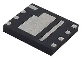


FDMS1D2N03DSD
Dual MOSFET, N Channel, 30 V, 164 A, 730 µohm, PQFN, Surface Mount
- Manufacturer: ONSEMI
- Product type: Dual MOSFETs
- No. of Pins: 8Pins
- Channel Type: N Channel
- Transistor Mounting: Surface Mount
- Transistor Polarity: N Channel
- Power Dissipation Pd: 42W
- Rds(on) Test Voltage: 10V
- On Resistance Rds(on): 730µohm
- Transistor Case Style: PQFN
- Drain Source Voltage Vds: 30V
- Operating Temperature Max: 150°C
- Continuous Drain Current Id: 164A
- Power Dissipation N Channel: 42W
- Power Dissipation P Channel: 42W
- Gate Source Threshold Voltage Max: 1.5V
- Drain Source Voltage Vds N Channel: 30V
- Drain Source Voltage Vds P Channel: 30V
- Continuous Drain Current Id N Channel: 164A
- Continuous Drain Current Id P Channel: 164A
- Drain Source On State Resistance N Channel: 730µohm
- Drain Source On State Resistance P Channel: 730µohm
| Delivery and price | |
|---|---|
| Units per pack | 500 |
| Price | 1.3 € |
| Current stock | 500+ |
| Lead time | 7 days |
## FDMS1D2N03DSD

## POWERTRENCH Power Clip 30 V Asymmetric Dual N‐Channel MOSFETs

## **General Description**

This device includes two specialized N-Channel MOSFETs in a dual package. The switch node has been internally connected to enable easy placement and routing of synchronous buck converters. The control MOSFET (Q1) and synchronous SyncFET (Q2) have been designed to provide optimal power efficiency.

## **www.onsemi.com**

## **ELECTRICAL CONNECTION**

## **Features**

## Q1: N-Channel

- Max RDS(on) = 3.25 m at VGS = 10 V, ID = 19 A

- Max RDS(on) = 4 m at VGS = 4.5 V, ID = 17 A

## Q2: N-Channel

- Max RDS(on) = 0.97 m Q at VGS = 10 V, ID = 37 A

- Max RDS(on) = 1.25 m at VGS = 4.5 V, ID = 34 A

**N-Channel MOSFET**

**==> picture [19 x 7] intentionally omitted <==**

**----- Start of picture text -----**<br>
PIN1<br>**----- End of picture text -----**<br>


- Low Inductance Packaging Shortens Rise/Fall Times, Resulting in Lower Switching Losses.

- MOSFET Integration Enables Optimum Layout for Lower Circuit Inductance and Reduced Switch Node Ringing.

- RoHS Compliant

Top View Bottom View

**Power Clip 56 (PQFN8 5x6) CASE 483AR**

## **Applications**

- Computing

## **PIN ASSIGNMENT**

- Communications

- General Purpose Point of Load

**==> picture [107 x 53] intentionally omitted <==**

**----- Start of picture text -----**<br>
HSG LSG<br>=o er 2<br>GR a SW<br>V+ sii} tf SW<br>V+ 4) tp Ld SW<br>*<br>PAD10<br>GND(LSS)<br>**----- End of picture text -----**<br>


*PAD9 V+(HSD)

## **MARKING DIAGRAM**

**==> picture [167 x 95] intentionally omitted <==**

**----- Start of picture text -----**<br>
$Y&Z&3&K<br>FDMS1D2<br>N03DSD<br>$Y = ON Semiconductor Logo<br>&Z = Assembly Plant Code<br>&3 = Numeric Date Code<br>&K = Lot Code<br>FDMS1D2N03DSD = Specific Device Code<br>**----- End of picture text -----**<br>


## **ORDERING INFORMATION**

See detailed ordering and shipping information on page 2 of this data sheet.

Publication Order Number: **FDMS1D2N03DSD/D**

**1**

© Semiconductor Components Industries, LLC, 2016 **May, 2018 − Rev. 5**

**FDMS1D2N03DSD**

**MOSFET MAXIMUM RATINGS** (TA = 25 ° C, Unless otherwise specified)

|**MOSFET MA**|**XIMUM RATINGS**(TA= 25°C, Unless otherwise specified)||||
|---|---|---|---|---|
|**Symbol**|**Parameter**|**Q1**|**Q2**|**Unit**|
|VDS|Drain to Source Voltage|30|30|V|
|VGS|Gate to Source Voltage|+16/−12|+16/−12|V|
|ID|Drain Current<br>−Continuous (TC= 25°C) (Note 5)|70|164|A|
||−Continuous (TC= 85°C) (Note 5)|54|126||
||−Continuous (TA= 25°C)|19 (Note 1a)|37 (Note 1b)||
||−Continuous (TA= 85°C)|15 (Note 1a)|29 (Note 1b)||
||−Pulsed (TA= 25°C) (Note 4)|362|1199||
|EAS|Single Pulsed Avalanche Energy (Note 3)|121|337|mJ|
|PD|Power Dissipation for Single Operation<br>(TC= 25°C)<br>(TA= 25°C)|26<br>2.1 (Note 1a)|42<br>2.3 (Note 1b)|W|
|TJ, TSTG|Operating and Storage Junction Temperature Range|−55 to +150||°C|


Stresses exceeding those listed in the Maximum Ratings table may damage the device. If any of these limits are exceeded, device functionality should not be assumed, damage may occur and reliability may be affected.

## **THERMAL CHARACTERISTICS**

|**Symbol**|**Parameter**|**Q1**|**Q2**|**Unit**|
|---|---|---|---|---|
|R�JC|Thermal Resistance, Junction to Case|4.8|3.0|�C/W|
|R�JA|Thermal Resistance, Junction to Ambient|60 (Note 1a)|55 (Note 1b)|�C/W|
|R�JA|Thermal Resistance, Junction to Ambient|130 (Note 1c)|120 (Note 1d)|�C/W|


## **PACKAGE MARKING AND ORDERING INFORMATION**

|**Device**|**Top Marking**|**Package**|**Reel Size**|**Tape Width**|**Quantity**|
|---|---|---|---|---|---|
|FDMS1D2N03DSD|FDMS1D2N03DSD|Power Clip 56 (PGFN8)<br>(Pb-Free / Halogen Free)|13″|12 mm|3,000 Units|


## **ELECTRICAL CHARACTERISTICS** (TJ = 25 ° C unless otherwise noted)

|**Symbol**|**Parameter**|**Test Conditions**|**Type**|**Min**|**Typ**|**Max**|**Unit**|
|---|---|---|---|---|---|---|---|
|**OFF CHARACTERISTICS**||||||||
|BVDSS|Drain to Source Breakdown Voltage|ID= 1 mA, VGS= 0 V|Q1<br>Q2|30<br>30|−<br>−|−<br>−|V|
|�BVDSS/�TJ|Breakdown Voltage Temperature<br>Coefficient|ID= 10 mA, referenced to 25�C|Q1<br>Q2|−<br>−|15<br>21|−<br>−|mV/�C|
|IDSS|Zero Gate Voltage Drain Current|VDS= 24 V, VGS= 0 V|Q1<br>Q2|−<br>−|−<br>−|1<br>500|�A|
|IGSS|Gate to Source Leakage Current,<br>Forward|VGS= +16 V/−12 V,<br>VDS= 0 V|Q1<br>Q2|−<br>−|−<br>−|±100<br>±100|nA<br>nA|
|**ON CHARACTERISTICS**||||||||
|VGS(th)|Gate to Source Threshold Voltage|VGS= VDS, ID= 320�A<br>VGS= VDS, ID= 1 mA|Q1<br>Q2|0.8<br>1.0|1.3<br>1.5|2.5<br>3.0|V|
|�VGS(th)/�TJ|Gate to Source Threshold Voltage<br>Temperature Coefficient|ID= 1 mA, referenced to 25�C<br>ID= 10 mA, referenced to 25�C|Q1<br>Q2|−<br>−|−3<br>−3|−<br>−|mV/�C|


**www.onsemi.com**

**2**

## **FDMS1D2N03DSD**

**ELECTRICAL CHARACTERISTICS** (TJ = 25 ° C unless otherwise noted)

|**ELECTRICAL**|**CHARACTERISTICS**(TJ= 25°C un|less otherwise noted)||||||
|---|---|---|---|---|---|---|---|
|**Symbol**|**Parameter**|**Test Conditions**|**Type**|**Min**|**Typ**|**Max**|**Unit**|
|**ON CHARACTERISTICS**||||||||
|RDS(on)|Drain to Source On Resistance|VGS= 10 V, ID= 19 A<br>VGS= 4.5 V, ID= 17 A<br>VGS= 10 V, ID= 19 A,<br>TJ=125�C|Q1|−<br>−<br>−|2.5<br>3.0<br>3.6|3.25<br>4.0<br>4.9|m�|
|||VGS= 10 V, ID= 37 A<br>VGS= 4.5 V, ID= 34 A<br>VGS= 10 V, ID= 37 A,<br>TJ=125�C|Q2|−<br>−<br>−|0.73<br>0.93<br>1.1|0.97<br>1.25<br>1.6||
|gFS|Forward Transconductance|VDS= 5 V, ID=  19 A<br>VDS= 5 V, ID=  37 A|Q1<br>Q2|−<br>−|95<br>247|−<br>−|S|
|**DYNAMIC CHARACTERISTICS**||||||||
|Ciss|Input Capacitance|Q1:<br>VDS= 15 V, VGS= 0 V,<br>f = 1 MHZ<br>Q2:<br>VDS= 15 V, VGS= 0 V,<br>f = 1 MHZ|Q1<br>Q2|−<br>−|1410<br>4860|−<br>−|pF|
|Coss|Output Capacitance||Q1<br>Q2|−<br>−|564<br>1845|−<br>−|pF|
|Crss|Reverse Transfer Capacitance||Q1<br>Q2|−<br>−|40<br>123|−<br>−|pF|
|Rg|Gate Resistance||Q1<br>Q2|−<br>−|0.3<br>0.3|−<br>−|�|
|**SWITCHING CHARACTERISTICS**||||||||
|td(on)|Turn-On Delay Time|Q1:<br>VDD= 15 V, ID= 19 A,<br>RGEN= 6�<br>Q2:<br>VDD= 15 V, ID= 37 A,<br>RGEN= 6�|Q1<br>Q2|−<br>−|8<br>13|−<br>−|ns|
|tr|Rise Time||Q1<br>Q2|−<br>−|2<br>5|−<br>−|ns|
|td(off)|Turn-Off Delay Time||Q1<br>Q2|−<br>−|22<br>37|−<br>−|ns|
|tf|Fall Time||Q1<br>Q2|−<br>−|2<br>4|−<br>−|ns|
|Qg|Total Gate Charge|VGS= 0 V to 10 V<br>Q1: VDD= 15 V, ID= 19 A<br>Q2: VDD= 15 V, ID= 37 A|Q1<br>Q2|−<br>−|23<br>84|33<br>117|nC|
|Qg|Total Gate Charge|VGS= 0 V to 4.5 V<br>Q1: VDD= 15 V, ID= 19 A<br>Q2: VDD= 15 V, ID= 37 A|Q1<br>Q2|−<br>−|11<br>39|15<br>54|nC|
|Qgs|Gate to Source Gate Charge|Q1: VDD= 15 V, ID= 19 A<br>Q2: VDD= 15 V, ID= 37 A|Q1<br>Q2|−<br>−|3.1<br>13|−<br>−|nC|
|Qgd|Gate to Drain “Miller” Charge|Q1: VDD= 15 V, ID= 19 A<br>Q2: VDD= 15 V, ID= 37 A|Q1<br>Q2|−<br>−|2.5<br>9|−<br>−|nC|
|**SOURCE-DRAIN DIODE CHARACTERISTICS**||||||||
|VSD|Source to Drain Diode Forward<br>Voltage|VGS= 0 V, IS= 19 A (Note 2)<br>VGS= 0 V, IS= 37 A (Note 2)|Q1<br>Q2|−<br>−|0.8<br>0.8|1.2<br>1.2|V|
|trr|Reverse Recovery Time|Q1:<br>IF= 19 A, di/dt = 100 A/�s<br>Q2:<br>IF= 37 A, di/dt = 300 A/�s|Q1<br>Q2|−<br>−|28<br>43|−<br>−|ns|
|Qrr|Reverse Recovery Charge||Q1<br>Q2|−<br>−|12<br>63|−<br>−|nC|


Product parametric performance is indicated in the Electrical Characteristics for the listed test conditions, unless otherwise noted. Product performance may not be indicated by the Electrical Characteristics if operated under different conditions.

**www.onsemi.com**

**3**

**FDMS1D2N03DSD**

NOTES:

1. R ts) JA is determined with the device mounted on a 1 in[2] pad 2 oz copper pad on a 1.5 × 1.5 in. board of FR−4 material. R 0 CA is determined by the user’s board design.

**==> picture [416 x 221] intentionally omitted <==**

**----- Start of picture text -----**<br>
a) 60 ° C/W when mounted on  b) 55 ° C/W when mounted on<br>a 1 in [2]  pad of 2 oz copper. a 1 in [2]  pad of 2 oz copper.<br>O) :<br>oooocd ooood<br>oooo0o0 oooco00<br>c) 130 ° C/W when mounted on  d) 120 ° C/W when mounted on<br>a minimum pad of 2 oz copper. a minimum pad of 2 oz copper.<br>3°<br>° ‘ tT<br>00000 oooo0co<br>G DF DS SF SS G DF DS SF SS<br>G DF DS SF SS G DF DS SF SS<br>**----- End of picture text -----**<br>


2. Pulse Test: Pulse Width < 300 s, Duty cycle < 2.0%. 0

3. Q1: EAS of 121 mJ is based on starting TJ = 25 ° C; N-ch: L = 3 mH, IAS = 9 A, VDD = 30 V. 100% tested at L = 0.1 mH, IAS = 29 A. Q2: EAS of 337 mJ is based on starting TJ = 25 C; N-ch: L = 3 mH, IAS = 15 A, VDD = 30 V. 100% tested at L = 0.1 mH, IAS = 47 A.

4. Pulsed Id please refer to Figure 11 and Figure 24 SOA graphs for more details.

5. Computed continuous current limited to Max Junction Temperature only, actual continuous current will be limited by thermal & electro-mechanical application board design.

**www.onsemi.com**

**4**

**FDMS1D2N03DSD**

## **TYPICAL CHARACTERISTICS (Q1 N-Channel)**

(TJ = 25 ° C unless otherwise noted)

**==> picture [212 x 556] intentionally omitted <==**

**----- Start of picture text -----**<br>
90<br>VGS = 10 V<br>75 V GS  = 4.5 V<br>VGS = 3.5 V<br>60<br>VGS = 3 V<br>45<br>30<br>VGS = 2.5 V<br>15 PULSE DURATION = 80 � s<br>DUTY CYCLE = 0.5% MAX<br>0<br>0.0 0.5 1.0 1.5 2.0<br>VDS, DRAIN TO SOURCE VOLTAGE (V)<br>Figure 1. On-Region Characteristics<br>1.8<br>ID = 19 A<br>1.6 V GS = 10 V<br>1.4<br>1.2<br>1.0<br>0.8<br>0.6<br>−75 −50 −25 0 25 50 75 100 125 150<br>TJ, JUNCTION TEMPERATURE ( � C)<br>Figure 3. Normalized On-Resistance vs.<br>Junction Temperature<br>90<br>PULSE DURATION = 80 � s<br>75 DUTY CYCLE = 0.5% MAX<br>VDS = 5 V<br>60<br>TJ = 150 [o] C<br>45<br>TJ = 25 [o] C<br>30<br>TJ = −55 [o] C<br>15<br>0<br>0 1 2 3 4<br>VGS, GATE TO SOURCE VOLTAGE (V)<br>, DRAIN CURRENT (A)<br>ID<br>NORMALIZED<br> DRAIN TO SOURCE ON−RESISTANCE<br>, DRAIN CURRENT (A)<br>ID<br>**----- End of picture text -----**<br>


**==> picture [210 x 150] intentionally omitted <==**

**----- Start of picture text -----**<br>
6.0<br>PULSE DURATION = 80 � s<br>DUTY CYCLE = 0.5% MAX<br>4.5<br>VGS = 2.5 V<br>3.0<br>VGS = 3 V<br>1.5<br>VGS = 3.5 V VGS = 4.5 V VGS = 10 V<br>0.0<br>0 15 30 45 60 75 90<br>ID, DRAIN CURRENT (A)<br>NORMALIZED<br>DRAIN TO SOURCE ON−RESISTANCE<br>**----- End of picture text -----**<br>


**Figure 2. Normalized On-Resistance vs. Drain Current and Gate Voltage**

**==> picture [214 x 354] intentionally omitted <==**

**----- Start of picture text -----**<br>
20<br>PULSE DURATION = 80 � s<br>DUTY CYCLE = 0.5% MAX<br>15<br>ID = 19 A<br>10<br>TJ = 125 [o] C<br>5<br>TJ = 25 [o] C<br>0<br>0 2 4 6 8 10<br>VGS, GATE TO SOURCE VOLTAGE (V)<br>Figure 4. On-Resistance vs. Gate to Source<br>Voltage<br>100<br>VGS = 0 V<br>10<br>1 TJ = 150 [o] C<br>TJ = 25 [ o] C<br>0.1<br>0.01 T J  = −55 [o] C<br>0.001<br>0.0 0.2 0.4 0.6 0.8 1.0 1.2<br>VSD, BODY DIODE FORWARD VOLTAGE (V)<br>) �<br>m<br> (<br>DRAIN TO<br>DS(on),<br>R<br>SOURCE ON−RESISTANCE<br>, REVERSE DRAIN CURRENT (A)<br>IS<br>**----- End of picture text -----**<br>


**Figure 5. Transfer Characteristics**

**Figure 6. Source to Drain Diode Forward Voltage vs. Source Current**

**www.onsemi.com**

**5**

**FDMS1D2N03DSD**

## **TYPICAL CHARACTERISTICS (Q1 N-Channel)**

(TJ = 25 ° C unless otherwise noted)

**==> picture [461 x 151] intentionally omitted <==**

**----- Start of picture text -----**<br>
10 10000<br>ID = 19 A<br>8 Ciss<br>VDD = 15 V<br>1000<br>6<br>VDD = 10 V VDD = 20 V Coss<br>4<br>100<br>2<br>f = 1 MHz VGS = 0 V C rss<br>0 10<br>0 5 10 15 20 25 0.1 1 10   30<br>Qg, GATE CHARGE (nC) VDS, DRAIN TO SOURCE VOLTAGE (V)<br>CAPACITANCE (pF)<br>, GATE TO SOURCE VOLTAGE (V)<br>GS<br>V<br>**----- End of picture text -----**<br>


**Figure 7. Gate Charge Characteristics**

**Figure 8. Capacitance vs. Drain to Source Voltage**

**==> picture [204 x 353] intentionally omitted <==**

**----- Start of picture text -----**<br>
50<br>TJ = 25 [ o] C<br>10 TJ = 100 [o] C<br>TJ = 125 [o] C<br>1<br>0.001 0.01 0.1 1 10 100<br>tAV, TIME IN AVALANCHE (ms)<br>Figure 9. Unclamped Inductive<br>Switching Capability<br>500<br>100 10  � s<br>10 100 � s<br>THIS AREA IS<br>LIMITED BY R<br>DS(on) 1 ms<br>SINGLE PULSE 10 ms<br>1<br>TJ = MAX RATED 100 ms<br>R � JC = 4.8 [ o] C/W CURVE BENT TO<br>TC = 25 [o] C MEASURED DATA<br>0.1<br>0.1 1 10 100<br>VDS, DRAIN to SOURCE VOLTAGE (V)<br>, AVALANCHE CURRENT (A)<br>IAS<br>, DRAIN CURRENT (A)<br>ID<br>**----- End of picture text -----**<br>


**==> picture [201 x 152] intentionally omitted <==**

**----- Start of picture text -----**<br>
80<br>64<br>VGS = 10 V<br>48<br>32 V GS = 4.5 V<br>16<br>R � JC = 4.8 [o] C/W<br>0<br>25 50 75 100 125 150<br>TC, CASE TEMPERATURE ( � C)<br>DRAIN CURRENT (A)<br>I,D<br>**----- End of picture text -----**<br>


**Figure 10. Maximum Continuous Drain Current vs. Case Temperature**

**==> picture [203 x 153] intentionally omitted <==**

**----- Start of picture text -----**<br>
10000<br>SINGLE PULSE<br>R � JC = 4.8 [o] C/W<br>1000 TC = 25 [o] C<br>100<br>10<br>10−5 10−4 10−3 10−2 10−1 1<br>t, PULSE WIDTH (sec)<br>PEAK TRANSIENT POWER (W)<br>(PK),<br>P<br>**----- End of picture text -----**<br>


**Figure 11. Forward Bias Safe Operating Area**

**Figure 12. Single Pulse Maximum Power Dissipation**

**www.onsemi.com**

**6**

**FDMS1D2N03DSD**

## **TYPICAL CHARACTERISTICS (Q1 N-Channel)**

(TJ = 25 ° C unless otherwise noted)

**==> picture [436 x 165] intentionally omitted <==**

**----- Start of picture text -----**<br>
2<br>DUTY CYCLE−DESCENDING ORDER<br>1<br>D = 0.5<br>      0.2<br>      0.1 PDM<br>0.1       0.05<br>      0.02<br>      0.01 t1<br>t 2<br>NOTES:<br>0.01<br>Z � JC(t) = r(t) x R � JC<br>SINGLE PULSE R � JC = 4.8 [o] C/W<br>Peak TJ = PDM x Z � JC(t) + TC<br>Duty Cycle, D = t1 / t2<br>0.001<br>10−5 10−4 10−3 10−2 10−1 1<br>t, RECTANGULAR PULSE DURATION (sec)<br>THERMAL RESISTANCE<br>r(t), NORMALIZED EFFECTIVE TRANSIENT<br>**----- End of picture text -----**<br>


**Figure 13. Junction-to-Case Transient Thermal Response Curve**

**www.onsemi.com**

**7**

**FDMS1D2N03DSD**

## **TYPICAL CHARACTERISTICS (Q2 N-Channel)**

(TJ = 25 ° C unless otherwise noted)

**==> picture [200 x 154] intentionally omitted <==**

**----- Start of picture text -----**<br>
180<br>VGS = 10 V<br>150 VGS = 4.5 V<br>VGS = 4 V<br>120<br>90<br>VGS = 3.5 V<br>60<br>VGS = 3 V<br>30 PULSE DURATION = 80 � s<br>DUTY CYCLE = 0.5% MAX<br>0<br>0.0 0.1 0.2 0.3 0.4 0.5 0.6<br>VDS, DRAIN TO SOURCE VOLTAGE (V)<br>, DRAIN CURRENT (A)<br>ID<br>**----- End of picture text -----**<br>


**Figure 14. On-Region Characteristics**

**==> picture [212 x 152] intentionally omitted <==**

**----- Start of picture text -----**<br>
4.5<br>PULSE DURATION = 80 � s<br>DUTY CYCLE = 0.5% MAX<br>3.6<br>VGS = 3 V<br>2.7<br>VGS = 3.5 V<br>1.8<br>0.9<br>VGS = 4 V VGS = 4.5 V VGS = 10 V<br>0.0<br>0 30 60 90 120 150 180<br>ID, DRAIN CURRENT (A)<br>NORMALIZED<br>DRAIN TO SOURCE ON−RESISTANCE<br>**----- End of picture text -----**<br>


**Figure 15. Normalized On-Resistance vs. Drain Current and Gate Voltage**

**==> picture [214 x 355] intentionally omitted <==**

**----- Start of picture text -----**<br>
1.8<br>ID = 37 A<br>1.6 V GS [=][ 10 V]<br>1.4<br>1.2<br>1.0<br>0.8<br>0.6<br>−75 −50 −25 0 25 50 75 100 125 150<br>TJ, JUNCTION TEMPERATURE ( � C)<br>Figure 16. Normalized On-Resistance vs.<br>Junction Temperature<br>180<br>PULSE DURATION = 80 � s<br>150 DUTY CYCLE = 0.5% MAX<br>VDS = 5 V<br>120<br>TJ = 125 [o] C<br>90<br>TJ = 25 [o] C<br>60<br>TJ = −55 [o] C<br>30<br>0<br>0 1 2 3 4<br>VGS, GATE TO SOURCE VOLTAGE (V)<br>NORMALIZED<br> DRAIN TO SOURCE ON−RESISTANCE<br>, DRAIN CURRENT (A)<br>ID<br>**----- End of picture text -----**<br>


**==> picture [209 x 353] intentionally omitted <==**

**----- Start of picture text -----**<br>
5<br>PULSE DURATION = 80 � s<br>DUTY CYCLE = 0.5% MAX<br>4<br>ID = 37 A<br>3<br>2<br>TJ = 125 [o] C<br>1<br>TJ = 25 [o] C<br>0<br>2 4 6 8    10<br>VGS, GATE TO SOURCE VOLTAGE (V)<br>Figure 17. On-Resistance vs. Gate to Source<br>Voltage<br>100<br>VGS = 0 V<br>10 TJ = 125 [o] C<br>1 TJ = 25 [ o] C<br>0.1 TJ = −55 [o] C<br>0.01<br>0.001<br>0.0 0.2 0.4 0.6 0.8 1.0<br>VSD, BODY DIODE FORWARD VOLTAGE (V)<br>) �<br>(m<br>DRAIN TO<br>DS(on),<br>R<br>SOURCE ON−RESISTANCE<br>, REVERSE DRAIN CURRENT (A)<br>IS<br>**----- End of picture text -----**<br>


**Figure 18. Transfer Characteristics**

**Figure 19. Source to Drain Diode Forward Voltage vs. Source Current**

**www.onsemi.com**

**8**

**FDMS1D2N03DSD**

## **TYPICAL CHARACTERISTICS (Q2 N-Channel)**

(TJ = 25 ° C unless otherwise noted)

**==> picture [461 x 151] intentionally omitted <==**

**----- Start of picture text -----**<br>
10 10000<br>ID = 37 A<br>8 C iss<br>VDD = 15 V 1000 Coss<br>6<br>VDD = 10 V<br>4<br>VDD = 20 V 100 Crss<br>2<br>f = 1 MHz<br>V GS = 0 V<br>0 10<br>0 20 40 60 80 100 0.1 1 10 30<br>Qg, GATE CHARGE (nC) VDS, DRAIN TO SOURCE VOLTAGE (V)<br>CAPACITANCE (pF)<br>, GATE TO SOURCE VOLTAGE (V)<br>GS<br>V<br>**----- End of picture text -----**<br>


**Figure 20. Gate Charge Characteristics**

**Figure 21. Capacitance vs. Drain to Source Voltage**

**==> picture [204 x 354] intentionally omitted <==**

**----- Start of picture text -----**<br>
100<br>TJ = 25 [ o] C<br>10 T J = 100 [o] C<br>T J  = 125 [o] C<br>1<br>0.001 0.01 0.1 1 10 100 1000<br>tAV, TIME IN AVALANCHE (ms)<br>Figure 22. Unclamped Inductive<br>Switching Capability<br>2000<br>1000<br>10  � s<br>100<br>10 THIS AREA IS  100  � s<br>LIMITED BY R<br>DS(on)<br>1 ms<br>SINGLE PULSE<br>1 TJ = MAX RATED 10 ms<br>R � JC [= 3.0] [ o] C/W CURVE BENT TO  100 ms<br>T C [= 25] [o] [C] MEASURED DATA<br>0.1<br>0.1 1 10 100<br>VDS, DRAIN to SOURCE VOLTAGE (V)<br>, AVALANCHE CURRENT (A)<br>IAS<br>, DRAIN CURRENT (A)<br>ID<br>**----- End of picture text -----**<br>


**==> picture [205 x 153] intentionally omitted <==**

**----- Start of picture text -----**<br>
180<br>144<br>VGS = 10 V<br>108<br>VGS = 4.5 V<br>72<br>36<br>R � JC = 3.0 [o] C/W<br>0<br>25 50 75 100 125 150<br>TC, CASE TEMPERATURE ( � C)<br>DRAIN CURRENT (A)<br>I,D<br>**----- End of picture text -----**<br>


**Figure 23. Maximum Continuous Drain Current vs. Case Temperature**

**==> picture [208 x 152] intentionally omitted <==**

**----- Start of picture text -----**<br>
100000<br>SINGLE PULSE<br>R � JC = 3.0 o C/W<br>10000<br>TC [= 25] [o] [C]<br>1000<br>100<br>10<br>10−5 10−4 10−3 10−2 10−1 1<br>t, PULSE WIDTH (sec)<br>PEAK TRANSIENT POWER (W)<br>(PK),<br>P<br>**----- End of picture text -----**<br>


**Figure 24. Forward Bias Safe Operating Area**

**Figure 25. Single Pulse Maximum Power Dissipation**

**www.onsemi.com**

**9**

**FDMS1D2N03DSD**

## **TYPICAL CHARACTERISTICS (Q2 N-Channel)**

(TJ = 25 ° C unless otherwise noted)

**==> picture [436 x 165] intentionally omitted <==**

**----- Start of picture text -----**<br>
2<br>DUTY CYCLE−DESCENDING ORDER<br>1<br>D = 0.5<br>      0.2<br>      0.1 PDM<br>0.1<br>      0.05<br>      0.02<br>      0.01 t 1<br>t2<br>0.01 NOTES:<br>Z � JC [(t) = r(t) x R] � JC<br>SINGLE PULSE R � JC  = 3.0 [o] C/W<br>Peak T J  = P DM  x Z � JC (t) + T C<br>Duty Cycle, D = t 1  / t 2<br>0.001<br>10−5 10−4 10−3 10−2 10−1 1<br>t, RECTANGULAR PULSE DURATION (sec)<br>THERMAL RESISTANCE<br>r(t), NORMALIZED EFFECTIVE TRANSIENT<br>**----- End of picture text -----**<br>


**Figure 26. Junction-to-Case Transient Thermal Response Curve**

**www.onsemi.com**

**10**

**FDMS1D2N03DSD**

## **TYPICAL CHARACTERISTICS** (continued)

## **SyncFET Schottky Body Diode Characteristics**

ON’s SyncFET process embeds a Schottky diode in parallel with PowerTrench MOSFET. This diode exhibits similar characteristics to a discrete external Schottky diode in parallel with a MOSFET. Figure 27 shows the reverse recovery characteristic of the FDMS1D2N03DSD.

Schottky barrier diodes exhibit significant leakage at high temperature and high reverse voltage. This will increase the power in the device.

**==> picture [201 x 152] intentionally omitted <==**

**----- Start of picture text -----**<br>
40<br>35<br>30<br>25<br>20<br>di/dt = 248 A/ � s<br>15<br>10<br>5<br>0<br>−5<br>100 200 300 400 500 600 700<br>TIME (ns)<br>CURRENT (A)<br>**----- End of picture text -----**<br>


**Figure 27. FDMS1D2N03DSD SyncFET Body Diode Reverse Recovery Characteristic**

**==> picture [204 x 154] intentionally omitted <==**

**----- Start of picture text -----**<br>
10−1<br>10−2 TJ = 125 [o] C<br>10−3<br>TJ = 100 [o] C<br>10−4<br>10−5 TJ = 25 [o] C<br>10−6<br>0 5 10 15 20 25 30<br>VDS, REVERSE VOLTAGE (V)<br>, REVERSE LEAKAGE CURRENT (A)<br>IDSS<br>**----- End of picture text -----**<br>


**Figure 28. SyncFET Body Diode Reverse Leakage vs. Drain-Source Voltage**

POWERTRENCH is a registered trademark and SyncFET is a trademark of Semiconductor Components Industries, LLC (SCILLC) or its subsidiaries in the United States and/or other countries.

**www.onsemi.com**

**11**

MECHANICAL CASE OUTLINE **PACKAGE DIMENSIONS**

**==> picture [78 x 29] intentionally omitted <==**

**----- Start of picture text -----**<br>
PQFN8 5X6, 1.27P<br>CASE 483AR<br>ISSUE O<br>**----- End of picture text -----**<br>


DATE 30 SEP 2016

**==> picture [491 x 629] intentionally omitted <==**

**----- Start of picture text -----**<br>
5.00<br>4.56<br>4.20<br>0.10 C 54.90.10 A<br>2X PKG 1.27<br>4 CL 1 B 4 3 2 1 3.30<br>2.48<br>2.08<br>1.01<br>6.60<br>PKG CL 6.105.90 0.00 2.65 0.400.83<br>1.43<br>1.98<br>2.48<br>0.82<br>3.30<br>PIN #1 5 8 0.10 C 5 6 7 8<br>2X<br>INDICATOR TOP VIEW 0.75<br>SEE<br>DETAIL A<br>RECOMMENDED LAND PATTERN<br>SIDE VIEW<br>3.15±.05 0.10 C A B<br>3.81 0.05 C<br>1.27<br>0.51<br>5 6 7 8 NOTES: UNLESS OTHERWISE SPECIFIED<br>0.65±.05 1.57±.05 A)  DOES NOT FULLY CONFORM TO<br>0.65±.05 JEDEC REGISTRATION, MO−229,<br>2.46±.05 DATED 11/2001.<br>1.37±.05 B)  ALL DIMENSIONS ARE IN<br>0.53±.05 MILLIMETERS.<br>0.91±.05 C)  DIMENSIONS DO NOT INCLUDE<br>0.48±.05 BURRS OR MOLD FLASH. MOLD<br>0.49±.05 4 3 2 1 FLASH OR BURRS DOES NOT<br>0.51±.05 EXCEED 0.10MM.<br>3 .90±.05 D)  DIMENSIONING AND TOLERANCING<br>4.22±.05 PER ASME Y14.5M−1994.<br>5.00±.05<br>BOTTOM VIEW<br>0.10 C<br>0.08 C<br>0.80 0.30 0.05 C<br>0.70 0.20 0.00 SEATING<br>PLANE<br>(SCALE: 2X)<br>DOCUMENT NUMBER: 98AON13666G Electronic versions are uncontrolled except when<br>accessed directly from the Document Repository. Printed<br>STATUS: ON SEMICONDUCTOR STANDARD<br>versions are uncontrolled except when stamped<br>“CONTROLLED COPY” in red.<br>NEW STANDARD:<br>©   Semiconductor Components Industries, LLC, 2002 http://onsemi.com Case Outline Number:<br>October, 2002 − Rev. 0DESCRIPTION: PQFN8 5X6, 1.27P 1 PAGE 1 OF 2XXX<br>1<br>1.53 1.0 0.00 1.08 1.48 1.53 2.29<br>**----- End of picture text -----**<br>


|**DOCUMENT NUMBER:**<br>**98AON13666G**<br>**PAGE 2 OF 2**<br>~~eT ©~~<br>~~——~~|**DOCUMENT NUMBER:**<br>**98AON13666G**<br>**PAGE 2 OF 2**<br>~~eT ©~~<br>~~——~~|
|---|---|
|**ISSUE**|**REVISION**<br>**DATE**|
|O|RELEASED FOR PRODUCTION FROM FAIRCHILD PQFN08K TO ON<br>30 SEP 2016|
||SEMICONDUCTOR. REQ. BY I. CAMBALIZA.|


**ON Semiconductor** and          are registered trademarks of Semiconductor Components Industries, LLC (SCILLC).  SCILLC reserves the right to make changes without further notice to any products herein.  SCILLC makes no warranty, representation or guarantee regarding the suitability of its products for any particular purpose, nor does SCILLC assume any liability arising out of the application or use of any product or circuit, and specifically disclaims any and all liability, including without limitation special, consequential or incidental damages. “Typical” parameters which may be provided in SCILLC data sheets and/or specifications can and do vary in different applications and actual performance may vary over time.  All operating parameters, including “Typicals” must be validated for each customer application by customer’s technical experts.  SCILLC does not convey any license under its patent rights nor the rights of others.  SCILLC products are not designed, intended, or authorized for use as components in systems intended for surgical implant into the body, or other applications intended to support or sustain life, or for any other application in which the failure of the SCILLC product could create a situation where personal injury or death may occur.  Should Buyer purchase or use SCILLC products for any such unintended or unauthorized application, Buyer shall indemnify and hold SCILLC and its officers, employees, subsidiaries, affiliates, and distributors harmless against all claims, costs, damages, and expenses, and reasonable attorney fees arising out of, directly or indirectly, any claim of personal injury or death associated with such unintended or unauthorized use, even if such claim alleges that SCILLC was negligent regarding the design or manufacture of the part.  SCILLC is an Equal Opportunity/Affirmative Action Employer.  This literature is subject to all applicable copyright laws and is not for resale in any manner.

Case Outline Number:

© Semiconductor Components Industries, LLC, 2016 **September, 2016 − Rev. O**

**483AR**

ON Semiconductor and      are trademarks of Semiconductor Components Industries, LLC dba ON Semiconductor or its subsidiaries in the United States and/or other countries. ON Semiconductor owns the rights to a number of patents, trademarks, copyrights, trade secrets, and other intellectual property. A listing of ON Semiconductor’s product/patent coverage may be accessed at www.onsemi.com/site/pdf/Patent−Marking.pdf. ON Semiconductor reserves the right to make changes without further notice to any products herein. ON Semiconductor makes no warranty, representation or guarantee regarding the suitability of its products for any particular purpose, nor does ON Semiconductor assume any liability arising out of the application or use of any product or circuit, and specifically disclaims any and all liability, including without limitation special, consequential or incidental damages. Buyer is responsible for its products and applications using ON Semiconductor products, including compliance with all laws, regulations and safety requirements or standards, regardless of any support or applications information provided by ON Semiconductor. “Typical” parameters which may be provided in ON Semiconductor data sheets and/or specifications can and do vary in different applications and actual performance may vary over time. All operating parameters, including “Typicals” must be validated for each customer application by customer’s technical experts. ON Semiconductor does not convey any license under its patent rights nor the rights of others. ON Semiconductor products are not designed, intended, or authorized for use as a critical component in life support systems or any FDA Class 3 medical devices or medical devices with a same or similar classification in a foreign jurisdiction or any devices intended for implantation in the human body. Should Buyer purchase or use ON Semiconductor products for any such unintended or unauthorized application, Buyer shall indemnify and hold ON Semiconductor and its officers, employees, subsidiaries, affiliates, and distributors harmless against all claims, costs, damages, and expenses, and reasonable attorney fees arising out of, directly or indirectly, any claim of personal injury or death associated with such unintended or unauthorized use, even if such claim alleges that ON Semiconductor was negligent regarding the design or manufacture of the part. ON Semiconductor is an Equal Opportunity/Affirmative Action Employer. This literature is subject to all applicable copyright laws and is not for resale in any manner.

## **PUBLICATION ORDERING INFORMATION**

## **LITERATURE FULFILLMENT** :

Literature Distribution Center for ON Semiconductor 19521 E. 32nd Pkwy, Aurora, Colorado 80011 USA **Phone** : 303−675−2175 or 800−344−3860 Toll Free USA/Canada **Fax** : 303−675−2176 or 800−344−3867 Toll Free USA/Canada **Email** : orderlit@onsemi.com

**N. American Technical Support** : 800−282−9855 Toll Free **ON Semiconductor Website** : **www.onsemi.com** USA/Canada

**Order Literature** : http://www.onsemi.com/orderlit For additional information, please contact your local Sales Representative

**Europe, Middle East and Africa Technical Support:** Phone: 421 33 790 2910

◊
Updated at February 9, 2023
onsemi is a premier global supplier of intelligent power and sensing technologies, driving disruptive innovations across the automotive, industrial, and cloud infrastructure markets. Recognized for their commitment to sustainability and reliable supply chains, the company accelerates advancements in vehicle electrification, industrial automation, and 5G networks by solving the industry's most complex design challenges. At the core of their portfolio is an industry-leading selection of discrete semiconductors. This extensive range features thousands of high-performance bipolar transistors, single and dual MOSFETs, and a comprehensive array of diodes, including Zener, Schottky, and fast-recovery rectifiers. Engineered for superior thermal performance and energy efficiency, these foundational components are critical for demanding power conversion, switching, and signal conditioning applications. Beyond essential discretes, onsemi provides a robust suite of advanced power management and circuit protection solutions. Their lineup includes intelligent power modules, single IGBTs, and transient voltage suppression (TVS) diodes designed to safeguard sensitive circuitry. Complimented by integrated passive filters, AC/DC LED driver ICs, and specialized sub-2.4GHz RF transceivers, onsemi equips engineers with the scalable, high-quality technologies needed to build a cleaner, smarter, and more connected world.
About Novapart
Novapart is a B2B electronic component broker specialising in stock shortages and cost reduction. We source hard-to-find parts and identify compliant alternatives across a catalogue of 410,000+ components from 500+ manufacturers.
Learn more →Stock Shortage Specialist
When a component is unavailable, discontinued or has an unacceptable lead time, we tap into our network of vetted European and Asian distributors to source what you need — without compromising on quality or traceability.
Request a quote →Compliant Alternatives
We identify pin-to-pin, electrically equivalent substitutes that meet the same certifications (RoHS, AEC-Q100, REACH) as your original specification — validated against datasheets, not just part numbers. Often at a lower cost.
BOM Analysis service →