
Image not available
Illustrative purposes only


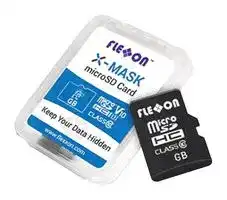
FDMM016GMG-XS00
Flash Memory Card, MicroSDHC Card, 16 GB
⚠️ Reference pricing provided. In case of supply shortages, we will connect you with our trusted procurement partners to ensure your project's continuity.
- Manufacturer: FLEXXON
- Product type: Flash Memory Cards
- SVHC: To Be Advised
- App Rating: -
- UHS Standard: -
- Product Range: X-Mask Series
- Memory Capacity: 16GB
- Video Speed Class: -
- Supply Voltage Nom: 3.3V
- Standard Speed Class: -
- Flash Memory Card Type: MicroSDHC Card
- Operating Temperature Max: 85°C
- Operating Temperature Min: -25°C
| Delivery and price | |
|---|---|
| Units per pack | 100 |
| Price | 24.4 € |
| Current stock | 10+ |
| Lead time | 30 days |
Datasheet

# **Industrial microSD 3.0 X-Mask Series (MLC)** ~~——$_~~ < **Version 1.2** Address: 28 Genting Ln, #09-03/04/05 Platinum 28, Singapore 349585 Tel: +65-6493 5035 Fax: +65-6493 5037 Website: http://www.flexxon.com Email: flexxon@flexxon.com ALL RIGHTS ARE STRICTLY RESERVED. ANY PORTION OF THIS PAPER SHALL NOT BE REPRODUCED, COPIED, OR TRANSLATED TO ANY OTHER FORMS WITHOUT PERMISSION FROM FLEXXON PTE LTD. ## **TABLE OF CONTENTS** ||**1. Contents**| |---|---| |**1.**|**GENERAL DESCRIPTION ................................................................................ 1**| ||Introduction ...................................................................................................................1<br>11| ||Product Overview ..........................................................................................................1<br>12| ||Workflow .......................................................................................................................2<br>13| |**2.**|**PRODUCT SPECIFICATIONS ........................................................................... 3**| ||Performance ...................................................................................................................3<br>2.1| ||Power .............................................................................................................................3<br>2.2| ||MTBF ............................................................................................................................3<br>2.3| |**3.**|**ENVIRONMENTAL SPECIFICATIONS ............................................................... 4**| |**4.**|**ELECTRICAL SPECIFICATIONS ........................................................................ 5**| ||DC Characteristics .........................................................................................................5<br>4.1| ||4.1.1<br>Bus Operation Conditions for 3.3V Signaling ................................................... 5| ||4.1.2<br>Bus Signal Line Load ........................................................................................ 6| ||AC Characteristic ..........................................................................................................7<br>4.2| ||4.2.1<br>microSD Interface timing (Default) .................................................................. 7| ||4.2.2<br>microSD Interface Timing (High-Speed Mode) ................................................ 8| |**5.**|4.2.3<br>microSD Interface timing (SDR12, SDR25, SDR50 and SDR104 Modes) .... 10<br>4.2.4<br>microSD Interface timing (DDR50 Modes) .................................................... 12<br>**PAD ASSIGNMENT ...................................................................................... 13**| |**6.** <br>**7.**|**REGISTERS .................................................................................................. 13**<br>**PHYSICAL DIMENSION ................................................................................ 13**| |**8.**|**ORDERING INFORMATION .......................................................................... 13**| ALL RIGHTS ARE STRICTLY RESERVED. ANY PORTION OF THIS PAPER SHALL NOT BE REPRODUCED, COPIED, OR TRANSLATED TO ANY OTHER FORMS WITHOUT PERMISSION FROM FLEXXON PTE LTD. ## **1. GENERAL DESCRIPTION** ## **Introduction** **FLEXXON X-Mask microSD Card** is compliant with SD 3.0 specification and provides excellent performance, good reliability and wide compatibility. User could mask the entire microSD card by special AP to prevent unauthorized access. **FLEXXON X-Mask microSD Card** provides security function to prevent the stored data from being stolen, tampered or modified by others. The stored data can only be access if the legitimate user can authenticate using the correct password. **FLEXXON X-Mask microSD Card** is suitable for users who want to store their private and valuable data in a flash storage without the risk of having it being read by unintended people. The mask function is an additional feature, which will not affect the standard product specification. **==> picture [70 x 28] intentionally omitted <==** **----- Start of picture text -----**<br> Product<br>Overview<br>**----- End of picture text -----**<br> - **Flash** **Support SD System** MLC **Specification 3.0** - **Capacity** **Support SD SPI Mode** 4GB to 128GB **Support Auto Read** - **Support Data Crypto Refreshment** - **Read disturbance** **Adaptive wear leveling** - **management** - **Support management of** **SMART function support** - **sudden power fails** - **Temperature Range** Operation (Gold): -25°C ~ 85°C Operation (Diamond): -40°C ~ 85°C - Storage: -40°C ~ 85°C 1 ALL RIGHTS ARE STRICTLY RESERVED. ANY PORTION OF THIS PAPER SHALL NOT BE REPRODUCED, COPIED, OR TRANSLATED TO ANY OTHER FORMS WITHOUT PERMISSION FROM FLEXXON PTE LTD. ## **Workflow** **FLEXXON X-Mask microSD Card** is a normal mode by default. User could set the password to enable mask mode. User is required to eject and re-insert the after set the password. User could access the data by the legal host with security tool and enter correct password. When user power off the host or reinsert the card, the card will return to masked mode. **==> picture [385 x 574] intentionally omitted <==** **----- Start of picture text -----**<br> Power On<br>Default Normal Mode<br>User use AP/ SDK to set password<br>Power Off/ unplug and plug in the card<br>Masked Mode<br>No<br>Legal Host?<br>Yes<br>Enter Password<br>No Correct<br>Password?<br>Yes<br>Normal Mode<br>Read/Write is possible,<br>Data Written is encrypted<br>and security controlled<br>z<br>Power Off<br>ALL RIGHTS ARE STRICTLY RESERVED. ANY PORTION OF THIS PAPER SHALL NOT BE REPRODUCED, COPIED,<br>OR TRANSLATED TO ANY OTHER FORMS WITHOUT PERMISSION FROM FLEXXON PTE LTD.<br>**----- End of picture text -----**<br> 2 ## **2. PRODUCT SPECIFICATIONS** | **==> picture [402 x 191] intentionally omitted <==** **----- Start of picture text -----**<br> Performance Capacity Sequential<br>Read (MB/s) Write (MB/s)<br>4GB 90 25<br>8GB 90 25<br>16GB 90 50<br>32GB 90 75<br>64GB 90 80<br>128GB 90 80<br>===<br>Table 2-1 Performance of X-Mask microSD<br>NOTES:<br>**----- End of picture text -----**<br> 1. The performance is obtained from TestMetrix 2. Performance may vary from flash configuration and platform. ## **Power** |**Capacity**|**Read**<br>**(mA)**|**Write**<br>**(mA)**|**Standby**<br>**(uA)**| |---|---|---|---| |4GB|180|90|220| |8GB|180|90|220| |16GB|190|120|250| |32GB|190|140|280| |64GB|190|170|320| |128GB|195|170|500| **Table 2-2 Typical Power Consumption of X-Mask microSD** ## **MTBF** MTBF, an acronym for Mean Time Between Failures, is a measure of a device’s reliability. Its value represents the average time between a repair and the next failure. The higher the MTBF value, the higher the reliability of the device. The predicted result of X-MASK microSD Card is more than 3,000,000 hours. 3 ALL RIGHTS ARE STRICTLY RESERVED. ANY PORTION OF THIS PAPER SHALL NOT BE REPRODUCED, COPIED, OR TRANSLATED TO ANY OTHER FORMS WITHOUT PERMISSION FROM FLEXXON PTE LTD. ## **3. ENVIRONMENTAL SPECIFICATIONS** |**Test Items**|**Test Conditions**| |---|---| |Storage Temperature|-40°C ~ 85°C| |Operating Temperature|Gold: -25°C ~ 85°C<br>Diamond: -40°C ~ 85°C| |Storage Humidity|40°C, 93% RH| |Operating Humidity|25°C, 95% RH| |Shock|1500G, Half Sin Pulse Duration 0.5ms| |Vibration|80Hz ~ 2000Hz/20G, 20Hz ~ 80Hz/1.52mm, 3<br>axis/30min| |Drop|150cm free fall, 6 face of each unit| |Bending|≥ 10N, Hold 1 min/5 times| |Torque|0.1N-m or +/-2.5 deg, Hold 30 seconds/5 times| |ESD|Contact: +/- 4KV each item 25 times<br>Air: +/- 8KV 10 times| **Table 3-1 Environmental Specification** 4 ALL RIGHTS ARE STRICTLY RESERVED. ANY PORTION OF THIS PAPER SHALL NOT BE REPRODUCED, COPIED, OR TRANSLATED TO ANY OTHER FORMS WITHOUT PERMISSION FROM FLEXXON PTE LTD. ## **4. ELECTRICAL SPECIFICATIONS** ## **DC Characteristics** ## **4.1.1 Bus Operation Conditions for 3.3V Signaling** |**Parameter**|**Symbol**|**Min.**|**Max**|**Unit**|**Condition**| |---|---|---|---|---|---| |SupplyVoltage|VDD|2.7|3.6|V|| |Output High Voltage|VOH|0.75*VDD||V|IOH=-2mA VDDMin| |Output Low Voltage|VOL||0.125*VDD|V|IOL=2mA VDDMin| |Input High Voltage|VIH|0.625*VDD|VDD+0.3|V|| |Input Low Voltage|VIL|VSS-0.3|0.25*VDD|V|| |Power Up Time|||250|ms|From 0V to VDDmin| **Table 4-1 Threshold Level for High Voltage Range** |**Parameter**|**Symbol**|**Min.**|**Max**|**Unit**|**Condition**| |---|---|---|---|---|---| |Supply Voltage|VDD|2.7|3.6|V|| |Regulator Voltage|VDDIO|1.7|1.95|V|Generated by VDD| |Output High Voltage|VOH|1.4|-|V|IOH=-2mA| |Output Low Voltage|VOL|-|0.45|V|IOL=2mA| |Input High Voltage|VIH|1.27|2.00|V|| |Input Low Voltage|VIL|Vss-0.3|0.58|V|| **Table 4-2 Threshold Level for 1.8V Signaling** |**Parameter**|**Symbol**|**Min**|**Max.**|**Unit**|**Remarks**| |---|---|---|---|---|---| |Input Leakage Current||-2|2|uA|DAT3 pull-up is<br>disconnected.| **Table 4-3 Input Leakage Current for 1.8V Signaling** 5 ALL RIGHTS ARE STRICTLY RESERVED. ANY PORTION OF THIS PAPER SHALL NOT BE REPRODUCED, COPIED, OR TRANSLATED TO ANY OTHER FORMS WITHOUT PERMISSION FROM FLEXXON PTE LTD. |**Parameter**|**Symbol**|**Min**|**Max.**|**Unit**|**Remarks**| |---|---|---|---|---|---| |Peak voltage on all lines||-0.3|VDD+0.3|V|| |**All Inputs**|||||| |Input Leakage Current||-10|10|uA|| |**All Outputs**|||||| |Output Leakage Current||-10|10|uA|| ## **Table 4-4 Peak Voltage and Leakage Current** ## **4.1.2 Bus Signal Line Load** ## **Bus Operation Conditions – Signal Line’s Load** Total Bus Capacitance = CHOST + CBUS + N CCARD |**Parameter**|**symbol**|**Min**|**Max**|**Unit**|**Remark**| |---|---|---|---|---|---| |Pull-up resistance|RCMD<br>RDAT|10|100|kΩ|to prevent bus floating| |Total bus capacitance for each<br>signal line|CL||40|pF|1 card<br>CHOST+CBUSshall<br>not exceed 30pF| |Card Capacitance for each signal<br>pin|CCARD||101|pF|| |Maximum signal line inductance|||16|nH|| |Pull-up resistance inside card<br>(pin1)|RDAT3|10|90|kΩ|May be used for card<br>detection| |Capacity Connected to Power<br>Line|CC||5|uF|To prevent inrush current| **Table 4-5 Peak Voltage and Leakage Current** 6 ALL RIGHTS ARE STRICTLY RESERVED. ANY PORTION OF THIS PAPER SHALL NOT BE REPRODUCED, COPIED, OR TRANSLATED TO ANY OTHER FORMS WITHOUT PERMISSION FROM FLEXXON PTE LTD. ## **AC Characteristic** ## **4.2.1 microSD Interface timing (Default)** 7 ALL RIGHTS ARE STRICTLY RESERVED. ANY PORTION OF THIS PAPER SHALL NOT BE REPRODUCED, COPIED, OR TRANSLATED TO ANY OTHER FORMS WITHOUT PERMISSION FROM FLEXXON PTE LTD. |**Parameter**|**Symbol**|**Min**|**Max**|**Unit**|**Remark**| |---|---|---|---|---|---| |**Clock CLK(All values are referred to min(VIH) and max(VIL)**|||||| |Clock frequency Data<br>Transfer Mode|fPP|0|25|MHz|Ccard≤ 10 pF<br>(1 card)| |Clock frequency<br>Identification Mode|fOD|0(1)/100|400|KHz|Ccard≤ 10 pF<br> (1 card)| |Clock low time|tWL|10||ns|Ccard≤ 10 pF<br> (1 card)| |Clock high time|tWH|10||ns|Ccard≤ 10 pF<br> (1 card)| |Clock rise time|tTLH||10|ns|Ccard≤ 10 pF<br> (1 card)| |Clock fall time|tTHL||10|ns|Ccard≤ 10 pF<br> (1 card)| |**Inputs CMD, DAT(referenced to CLK)**|||||| |Input set-up time|tISU|5||ns|Ccard≤ 10 pF<br> (1 card)| |Input hold time|tIH|5||ns|Ccard≤ 10 pF<br> (1 card)| |**Outputs CMD, DAT(referenced to CLK)**|||||| |Output Delay time during<br>Data Transfer Mode|tODLY|0|14|ns|CL≤ 40 pF<br>(1 card)| |Output Delay time during<br>Identification Mode|tODLY|0|50|ns|CL≤ 40 pF<br>(1 card)| - (1) 0Hz means to stop the clock. The given minimum frequency range is for cases where continues clock is required. ## **4.2.2 microSD Interface Timing (High-Speed Mode)** 8 ALL RIGHTS ARE STRICTLY RESERVED. ANY PORTION OF THIS PAPER SHALL NOT BE REPRODUCED, COPIED, OR TRANSLATED TO ANY OTHER FORMS WITHOUT PERMISSION FROM FLEXXON PTE LTD. |**Parameter**|**Symbol**|**Min**|**Max**|**Unit**|**Remark**| |---|---|---|---|---|---| |**Clock CLK(All values are referred to min(VIH) and max(VIL)**|||||| |Clock frequency Data Transfer<br>Mode|fPP|0|50|MHz|Ccard≤ 10 pF<br>(1 card)| |Clock low time|tWL|7||ns|Ccard≤ 10 pF<br> (1 card)| |Clock high time|tWH|7||ns|Ccard≤ 10 pF<br> (1 card)| |Clock rise time|tTLH||3|ns|Ccard≤ 10 pF<br> (1 card)| |Clock fall time|tTHL||3|ns|Ccard≤ 10 pF<br> (1 card)| |**Inputs CMD, DAT(referenced to CLK)**|||||| |Input set-up time|tISU|6||ns|Ccard≤ 10 pF<br> (1 card)| |Input hold time|tIH|2||ns|Ccard≤ 10 pF<br> (1 card)| |**Outputs CMD, DAT(referenced to CLK)**|||||| |Output Delay time during Data<br>Transfer Mode|tODLY||14|ns|CL≤ 40 pF<br>(1 card)| |Output Hold time|TOH|2.5||ns|CL≤ 15 pF<br>(1 card)| |Total System capacitance of<br>each line¹|CL||40|pF|CL ≤ 15 pF<br>(1 card)| (1) In order to satisfy severe timing, the host shall drive only one card. 9 ALL RIGHTS ARE STRICTLY RESERVED. ANY PORTION OF THIS PAPER SHALL NOT BE REPRODUCED, COPIED, OR TRANSLATED TO ANY OTHER FORMS WITHOUT PERMISSION FROM FLEXXON PTE LTD. ## **4.2.3 microSD Interface timing (SDR12, SDR25, SDR50 and SDR104 Modes)** ## _**Input:**_ |**Symbol**|**Min**|**Max**|**Unit**|**Remark**| |---|---|---|---|---| |tCLK|4.80|-|ns|208MHz (Max.), Between rising edge, VCT=<br>0.975V| |tCR, tCF|-|0.2* tCLK|ns|tCR, tCF< 0.96ns (max.) at 208MHz, CCARD=10pF<br>tCR, tCF< 2.00ns (max.) at 100MHz, CCARD=10pF<br>The absolute maximum value of tCR, tCFis 10ns<br>regardless of clock frequency| |Clock Duty|30|70|%|| ## **SDR50 and SDR104 Input Timing:** |**Symbol**|**Min**|**Max**|**Unit**|**SDR104 Mode**| |---|---|---|---|---| |tIS|1.40|-|ns|CCARD=10pF,VCT= 0.975V| |tIH|0.8|-|ns|CCARD= 5pF,VCT= 0.975V| |**Symbol**|**Min**|**Max**|**Unit**|**SDR50 Mode**| |tIS|3.00|-|ns|CCARD=10pF,VCT= 0.975V| |tIH|0.8|-|ns|CCARD= 5pF,VCT= 0.975V| 10 ALL RIGHTS ARE STRICTLY RESERVED. ANY PORTION OF THIS PAPER SHALL NOT BE REPRODUCED, COPIED, OR TRANSLATED TO ANY OTHER FORMS WITHOUT PERMISSION FROM FLEXXON PTE LTD. ## _**Output**_ **(SDR12, SDR25, SDR50)** _**:**_ |**Symbol**|**Min**|**Max**|**Unit**|**Remark**| |---|---|---|---|---| |tODLY|-|7.5|ns|tCLK>=10.0ns,CL=30pF,usingdriver Type B,for SDR50| |tODLY|-|14|ns|tCLK>=20.0ns, CL=40pF, using driver Type B, for SDR25<br>and SDR12,| |TOH|1.5|-|ns|Hold time at the tODLY (min.),CL=15pF| ## _**Output (SDR104 Mode):**_ |**Symbol**|**Min**|**Max**|**Unit**|**Remark**| |---|---|---|---|---| |tOP|0|2|Ul|Card Output Phase| |△tOP|-350|+1550|ps|Delayvariable due to temperature change after tuning| |tODW|0.60|-|Ul|tODW= 2.88ns at 208MHz| 11 ALL RIGHTS ARE STRICTLY RESERVED. ANY PORTION OF THIS PAPER SHALL NOT BE REPRODUCED, COPIED, OR TRANSLATED TO ANY OTHER FORMS WITHOUT PERMISSION FROM FLEXXON PTE LTD. ## **4.2.4 microSD Interface timing (DDR50 Modes)** |**Symbol**|**Min**|**Max**|**Unit**|**Remark**| |---|---|---|---|---| |tCLK|20|-|ns|50MHz(Max.),Between risingedge| |tCR,tCF|-|0.2* tCLK|ns|tCR,tCF< 4.00ns(max.)at 50MHz,CCARD=10pF| |Clock Duty|45|55|%|| 12 ALL RIGHTS ARE STRICTLY RESERVED. ANY PORTION OF THIS PAPER SHALL NOT BE REPRODUCED, COPIED, OR TRANSLATED TO ANY OTHER FORMS WITHOUT PERMISSION FROM FLEXXON PTE LTD. |**Parameter**<br>~~a~~|**Symbol**|**Min**|**Max**|**Unit**|**Remark**| |---|---|---|---|---|---| |**Input CMD**(referenced to CLK risingedge)<br>~~a~~<br>~~eeeeeeee~~<br>~~a~~|||||| |Input set-up time<br>~~a~~<br>~~a~~|tISU<br>~~ee~~<br>~~a~~|3<br>~~ee~~<br>~~ee~~|-<br>~~ee~~<br>~~ee~~|ns<br>~~ee~~<br>~~ee~~|Ccard≤ 10 pF<br> (1 card)<br>~~ee~~| |Input hold time<br>~~a ~~|tIH<br>~~ee ~~<br> ~~a~~|0.8<br> ~~ee~~<br>~~ee~~|-<br>~~ee ~~<br>~~ee~~|ns<br> ~~ee ~~<br>~~ee~~|Ccard≤ 10 pF<br> (1 card)<br> ~~ee~~| |**Output CMD**(referenced to CLK risingedge)<br> ~~a~~<br>~~ee ee~~|||||| |Output Delay time<br>during Data Transfer<br>Mode<br>~~a~~|tODLY<br>~~ee~~|~~ee~~|13.7<br>~~ee~~|ns<br>~~ee~~|CL≤ 30 pF<br>(1 card)| |Output Hold time<br>~~a~~|TOH<br>~~ee~~|1.5<br>~~ee~~|-<br>~~ee~~|ns<br>~~ee~~<br>~~NS~~|CL≥ 15 pF<br>(1 card)<br>~~NS~~| |**Inputs DAT**(referenced to CLK risingand fallingedges)<br>~~a ee~~<br>~~ee~~<br>~~ee~~<br>~~NS~~<br>~~eeee~~<br>~~ee~~|||||| |Input set-up time<br>~~es~~|tISU2x<br>~~es~~<br>~~ee~~<br>~~ee~~|3<br>~~es~~<br>~~ee~~<br>~~ee~~|-<br>~~es~~<br>~~ee~~<br>~~ee~~|ns<br>~~NS~~<br>~~es~~<br>~~ee~~|Ccard≤ 10 pF<br> (1 card)<br>~~NS~~<br>~~es~~<br>~~ee~~| |Input hold time<br>~~re~~|tIH2x<br>~~ee~~<br>~~re~~<br>~~ee~~|0.8<br>~~ee ~~<br>~~re~~<br>~~ee~~|-<br> ~~ee~~<br>~~re~~<br>~~ee~~|ns<br>~~ee~~<br>~~re~~|Ccard≤ 10 pF<br> (1 card)<br>~~ee~~<br>~~re~~| |**Outputs DAT**(referenced to CLK risingand fallingedges)<br>~~re~~<br>~~ee ee~~|||||| |Output Delay time<br>during Data Transfer<br>Mode|tODLY2x|-|7.0|ns|CL≤ 25 pF<br>(1 card)<br>~~ee~~| |Output Hold time<br>~~a ee~~|TOH2x<br>~~ee~~|1.5<br>~~ee~~|-<br>~~ee~~|ns<br>~~ee~~|CL≥ 15 pF<br>(1 card)<br>~~ee~~<br>~~ee~~| **Table 4-6 Bus Timings – Parameters Values (DDR50 Mode)** 13 ALL RIGHTS ARE STRICTLY RESERVED. ANY PORTION OF THIS PAPER SHALL NOT BE REPRODUCED, COPIED, OR TRANSLATED TO ANY OTHER FORMS WITHOUT PERMISSION FROM FLEXXON PTE LTD. ## **5. PAD ASSIGNMENT** Ps **==> picture [441 x 189] intentionally omitted <==** **----- Start of picture text -----**<br> SD Mode SPI Mode<br>Pin #<br>Name Type [1] Description Name Type Description<br>1 DAT2 I/O/PP Data Line[bit2] RSV<br>Fs 2 CD/DAT3 [2] I/O/PP [3] Card Detect/ Data CS I [3] Chip Select (neg<br>Line[bit3] true)<br>ee 3 CMD ee PP Command/Response DI I Data In<br>aeeee eee<br>FG 4 VDD S Supply voltage SO VDD S Supply voltage<br>5 CLK I Clock SCLK I Clock<br>LO<br>6 VSS S Supply voltage VSS S Supply voltage<br>ground ground<br>ssee 7 DAT0 I/O/PP ee Data Line[bit0] eee DO O/PP Data Out<br>Qs 8 DAT1 I/O/PP Data Line[bit1] RSV<br>**----- End of picture text -----**<br> **Table 5-1 microSD Pad Assignment** ## **NOTE:** - (1) S: power supply, I: input; O: output using push-pull drivers; PP: I/O using push-pull drivers - (2) The extended DAT lines (DAT1-DAT3) are input on power up. They start to operate as DAT lines after SET_BUS_WIDTH command. The Host shall keep its own DAT1-DAT3 lines in input mode, as well, while they are not used. It is defined so, in order to keep compatibility to MultiMedia Cards. - (3) At power up this line has a 50KOhm pull up enabled in the card. This resistor serves two functions: Card detection and Mode Selection. For Mode Selection, the host can drive the line high or let it be pulled high to select SD mode. If the host wants to select SPI mode it should drive the line low. For Card detection, the host detects that the line is pulled high. This pull-up should be disconnected by the user during regular data transfer period, with SET_CLR_CARD_DETECT (ACMD42) command. 14 ALL RIGHTS ARE STRICTLY RESERVED. ANY PORTION OF THIS PAPER SHALL NOT BE REPRODUCED, COPIED, OR TRANSLATED TO ANY OTHER FORMS WITHOUT PERMISSION FROM FLEXXON PTE LTD. ## **6. REGISTERS** |**Name**|**Width**|**Description**| |---|---|---| |CID|128bit|Card identification number; card individual number for<br>identification.| |RCA|16bit|Relative card address; local system address of a card,<br>dynamically suggested by the card and approved by the host<br>duringinitialization.| |DSR|16bit|Driver Stage Register; to configure the card’s output drivers.| |CSD|128bit|Card Specific Data; Information about the card operation<br>conditions.| |SCR|64bit|SD Configuration Register; Information about the SD<br>MemoryCard's Special Features capabilities| |OCR|32bit|Operation conditions register.| |SSR|512bit|SD Status; Information about the card proprietary features.| |OCR|32bit|Card Status; Information about the card status.| **Table 6-1 microSD Registers** 15 ALL RIGHTS ARE STRICTLY RESERVED. ANY PORTION OF THIS PAPER SHALL NOT BE REPRODUCED, COPIED, OR TRANSLATED TO ANY OTHER FORMS WITHOUT PERMISSION FROM FLEXXON PTE LTD. ## **7. PHYSICAL DIMENSION** ## **Dimension: 15mm (L) x 11mm (W) x 1mm (H)** ## Top View **==> picture [60 x 225] intentionally omitted <==** **----- Start of picture text -----**<br> Bottow View<br>Side View<br>**----- End of picture text -----**<br> 16 ALL RIGHTS ARE STRICTLY RESERVED. ANY PORTION OF THIS PAPER SHALL NOT BE REPRODUCED, COPIED, OR TRANSLATED TO ANY OTHER FORMS WITHOUT PERMISSION FROM FLEXXON PTE LTD. 17 ALL RIGHTS ARE STRICTLY RESERVED. ANY PORTION OF THIS PAPER SHALL NOT BE REPRODUCED, COPIED, OR TRANSLATED TO ANY OTHER FORMS WITHOUT PERMISSION FROM FLEXXON PTE LTD. ## **8. ORDERING INFORMATION** |**Capacity**|**MPN(Diamond Grade)**|**MPN (Gold Grade)**| |---|---|---| |4GB|FDMM004GME-XS00|FDMM004GMG-XS00| |8GB|FDMM008GME-XS00|FDMM008GMG-XS00| |16GB|FDMM016GME-XS00|FDMM016GMG-XS00| |32GB|FDMM032GME-XS00|FDMM032GMG-XS00| |64GB|FDMM064GME-XS00|FDMM064GMG-XS00| |128GB|FDMM128GME-XS00|FDMM128GMG-XS00| 18 ALL RIGHTS ARE STRICTLY RESERVED. ANY PORTION OF THIS PAPER SHALL NOT BE REPRODUCED, COPIED, OR TRANSLATED TO ANY OTHER FORMS WITHOUT PERMISSION FROM FLEXXON PTE LTD. ## **REVISION HISTORY** |**Revision**|**Date**|**History**| |---|---|---| |1.0|2020/08|First Release| |1.1|2020/09|Update Chapter 1| |1.2|2020/11|Update Workflow| 19 ALL RIGHTS ARE STRICTLY RESERVED. ANY PORTION OF THIS PAPER SHALL NOT BE REPRODUCED, COPIED, OR TRANSLATED TO ANY OTHER FORMS WITHOUT PERMISSION FROM FLEXXON PTE LTD.
Updated at June 3, 2026
About Novapart
Novapart is a B2B electronic component broker specialising in stock shortages and cost reduction. We source hard-to-find parts and identify compliant alternatives across a catalogue of 410,000+ components from 500+ manufacturers.
Learn more →Stock Shortage Specialist
When a component is unavailable, discontinued or has an unacceptable lead time, we tap into our network of vetted European and Asian distributors to source what you need — without compromising on quality or traceability.
Request a quote →Compliant Alternatives
We identify pin-to-pin, electrically equivalent substitutes that meet the same certifications (RoHS, AEC-Q100, REACH) as your original specification — validated against datasheets, not just part numbers. Often at a lower cost.
BOM Analysis service →