
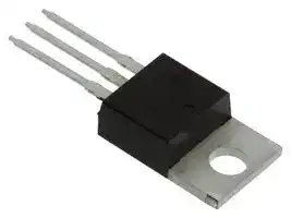


FCP190N60-GF102
Power MOSFET, N Channel, 600 V, 20.2 A, 0.199 ohm, TO-220, Through Hole
- Manufacturer: ONSEMI
- Product type: Single MOSFETs
- SVHC: No SVHC (15-Jan-2018)
- No. of Pins: 3Pins
- Channel Type: N Channel
- Product Range: SuperFET II
- Qualification: -
- Power Dissipation: 208W
- Transistor Mounting: Through Hole
- Rds(on) Test Voltage: 10V
- Transistor Case Style: TO-220
- Drain Source Voltage Vds: 600V
- Operating Temperature Max: 150°C
- Continuous Drain Current Id: 20.2A
- Drain Source On State Resistance: 0.199ohm
- Gate Source Threshold Voltage Max: 3.5V
| Delivery and price | |
|---|---|
| Units per pack | 800 |
| Price | 1.41 € |
| Current stock | 10+ |
| Lead time | 30 days |
## **Is Now Part of**

## **To learn more about ON Semiconductor, please visit our website at www.onsemi.com**

Please note: As part of the Fairchild Semiconductor integration, some of the Fairchild orderable part numbers will need to change in order to meet ON Semiconductor’s system requirements. Since the ON Semiconductor product management systems do not have the ability to manage part nomenclature that utilizes an underscore (_), the underscore (_) in the Fairchild part numbers will be changed to a dash (-). This document may contain device numbers with an underscore (_). Please check the ON Semiconductor website to verify the updated device numbers. The most current and up-to-date ordering information can be found at www.onsemi.com. Please email any questions regarding the system integration to Fairchild_questions@onsemi.com.

ON Semiconductor and the ON Semiconductor logo are trademarks of Semiconductor Components Industries, LLC dba ON Semiconductor or its subsidiaries in the United States and/or other countries. ON Semiconductor owns the rights to a number of patents, trademarks, copyrights, trade secrets, and other intellectual property. A listing of ON Semiconductor’s product/patent coverage may be accessed at www.onsemi.com/site/pdf/Patent-Marking.pdf. ON Semiconductor reserves the right to make changes without further notice to any products herein. ON Semiconductor makes no warranty, representation or guarantee regarding the suitability of its products for any particular purpose, nor does ON Semiconductor assume any liability arising out of the application or use of any product or circuit, and specifically disclaims any and all liability, including without limitation special, consequential or incidental damages. Buyer is responsible for its products and applications using ON Semiconductor products, including compliance with all laws, regulations and safety requirements or standards, regardless of any support or applications information provided by ON Semiconductor. “Typical” parameters which may be provided in ON Semiconductor data sheets and/or specifications can and do vary in different applications and actual performance may vary over time. All operating parameters, including “Typicals” must be validated for each customer application by customer’s technical experts. ON Semiconductor does not convey any license under its patent rights nor the rights of others. ON Semiconductor products are not designed, intended, or authorized for use as a critical component in life support systems or any FDA Class 3 medical devices or medical devices with a same or similar classification in a foreign jurisdiction or any devices intended for implantation in the human body. Should Buyer purchase or use ON Semiconductor products for any such unintended or unauthorized application, Buyer shall indemnify and hold ON Semiconductor and its officers, employees, subsidiaries, affiliates, and distributors harmless against all claims, costs, damages, and expenses, and reasonable attorney fees arising out of, directly or indirectly, any claim of personal injury or death associated with such unintended or unauthorized use, even if such claim alleges that ON Semiconductor was negligent regarding the design or manufacture of the part. ON Semiconductor is an Equal Opportunity/Affirmative Action Employer. This literature is subject to all applicable copyright laws and is not for resale in any manner.

## **December 2013**

## **N-Channel SuperFET[®] II MOSFET**

## **600 V, 20.2 A, 199 m** Ω

## **Features**

- 650 V @ TJ = 150°C

- Typ. RDS(on) = 170 m Ω

- Ultra Low Gate Charge (Typ. Qg = 57 nC)

- Low Effective Output Capacitance (Typ. Coss(eff.) = 160 pF)

- 100% Avalanche Tested

- RoHS Compliant

## **Application**

## **Description**

SuperFET[®] II MOSFET is Fairchild Semiconductor’s brand-new high voltage super-junction (SJ) MOSFET family that is utilizing charge balance technology for outstanding low on-resistance and lower gate charge performance. This technology is tailored to minimize conduction loss, provide superior switching performance, dv/dt rate and higher avalanche energy. Consequently, SuperFET II MOSFET is very suitable for the switching power applications such as PFC, server/telecom power, FPD TV power, ATX power and industrial power applications.

- LCD / LED / PDP TV Lighting

- Solar Inverter

- AC-DC Power Supply

**==> picture [225 x 96] intentionally omitted <==**

**----- Start of picture text -----**<br>
D<br>GDS G<br>TO-220<br>S<br>**----- End of picture text -----**<br>


**Absolute Maximum Ratings** TC = 25[o] C unless otherwise noted.

|**Absolute Maximum Ratings**<br>~~es~~|**Absolute Maximum Ratings  **TC = 25C = 25= 25[o]C unless otherwise noted.|**Absolute Maximum Ratings  **TC = 25C = 25= 25[o]C unless otherwise noted.|||
|---|---|---|---|---|
|**Symbol**<br>~~es~~<br>~~—————~——_~~|**Parameter**<br>**FCP190N60**<br>~~—————~——_~~<br>~~...©80..—SOlldCNdN)d)s)s§s§s§$:$s§s§s$$':$»=—Z”2z=_~~||**FCP190N60_GF102**<br>~~»=—Z”2z=_7~~|**Unit**|
|VDSS<br>~~es~~<br>~~—————~——_~~|Drain to Source Voltage<br>~~—————~——_~~<br>~~...©80..—SOlldCNdN)d)s)s§s§s§$:$s§s§s$$':$»=—Z”2z=_~~<br>~~a~~||600<br>~~»=—Z”2z=_7~~|V|
|VGSS<br>~~—————~——_~~|Gate to Source Voltage<br>~~—————~——_~~<br>~~. . ~~<br>~~a~~<br>~~a~~|- DC<br> ~~.©80..—SOlldCN dN) d)s)s§s§s§$:$s§s§s$$':$ »=—Z”2z=_~~<br>~~a~~|±20<br>~~»=—Z”2z=_7~~|V|
|||- AC                                                    (f > 1 Hz)<br>~~a~~<br>~~a~~|±30||
|ID|Drain Current<br>~~a~~<br>~~|~~|- Continuous (TC= 25oC)<br>~~a~~<br>~~|~~<br>~~...... »»»#_,~f~~~|20.2<br>~~ry|~~|A<br>~~|~~|
|||- Continuous(TC= 100oC)<br>~~a~~<br>~~|~~<br>~~...... »»»#_,~f~~~|12.7<br>~~ry|~~||
|IDM|Drain Current<br>~~|~~<br>~~”|)3]|=)3—COC——“‘“‘—sOS:—<“—<—C~C~~|- Pulsed(Note 1)<br>~~|~~<br>~~......  »» » # _,~f~ ~~<br>~~”|)3]|=)3—COC——“‘“‘—sOS:—<“—<—C~C~~|60.6<br> ~~ry |~~<br>~~”|)3]|=)3—COC——“‘“‘—sOS:—<“—<—C~C~~|A<br>~~|~~<br>~~”|)3]|=)3—COC——“‘“‘—sOS:—<“—<—C~C~~|
|EAS|Single Pulsed Avalanche Energy (Note 2)<br>~~|©—lt—“‘“COC~‘CONONOCCtitsi‘<(‘(“(‘C~~||400<br>~~|©—lt—“‘“COC~‘CONONOCCtitsi‘<(‘(“(‘C~~|mJ<br>~~|©—lt—“‘“COC~‘CONONOCCtitsi‘<(‘(“(‘C~~|
|IAR<br>~~x~~|Avalanche Current(Note 1)<br>~~LTE-—=S—=—“—~~<br>~~x~~||4.0<br>~~LTE-—=S—=—“—~~<br>~~==—«.~~|A<br>~~LTE-—=S—=—“—~~<br>~~=—«.~~|
|EAR<br>~~OO~~<br>~~x~~<br>~~__~~|Repetitive Avalanche Energy (Note 1)<br>~~OO~~<br>~~x~~<br>~~OSL~~<br>~~__~~||2.1<br>~~OO~~<br>~~==—«.~~<br>~~OSL~~<br>~~2~~<br>|mJ<br>~~OO~~<br>~~=—«.~~|
|dv/dt<br>~~x~~<br>~~__~~|MOSFET dv/dt<br>~~x~~<br>——ti‘“‘CWWOWUOU™€™€™F€™€™€™~*~™.U~C~COCOC<br>~~OSL~~<br>~~__~~<br>~~|~~||100<br>~~==—«.~~<br>——ti‘“‘CWWOWUOU™€™€™F€™€™€™~*~™.U~C~COCOC<br>~~OSL~~<br>~~2~~<br><br>~~|fa”7~~|V/ns<br>~~=—«.~~<br>~~2~~|
||Peak Diode Recoverydv/dt(Note 3)<br>~~x~~<br>~~OSL~~<br>~~__|~~<br>~~|~~<br>~~—~~<br>~~i2~~||20<br>~~==—«.~~<br>~~OSL~~<br>~~2~~<br>~~|~~<br>~~|fa”7~~<br>~~2~~||
|PD<br>~~__~~<br>~~i.~~<br>~~es~~|Power Dissipation<br>~~__~~<br>~~i.~~|(TC= 25oC)<br>~~OSL~~<br><br>~~|~~<br>~~i.~~<br>~~—~~<br>~~i2~~|208<br>~~OSL~~<br>~~2~~<br><br>~~| fa” 7~~<br>~~i.~~<br>~~2~~|W<br>~~i.~~<br>~~2~~|
|||- Derate Above 25oC<br>~~i.~~<br>~~—~~<br>~~i2~~<br>~~a~~|1.67<br>~~i.~~<br>~~2~~<br>~~a~~|W/oC<br>~~i.~~<br>~~2~~<br>~~a~~|
|TJ, TSTG<br>~~es~~<br>~~es~~|Operatingand Storage Temperature Range<br>~~—~~<br>~~i 2~~<br>~~a~~||-55 to +150<br>~~2~~<br>~~a~~|oC<br>~~2~~<br>~~a~~|
|TL<br>~~es~~<br>~~es~~|Maximum Lead Temperature for Soldering, 1/8” from Case for 5 Seconds<br>~~a~~||300<br>~~a~~|oC<br>~~a~~|


www.fairchildsemi.com

©2013 Fairchild Semiconductor Corporation FCP190N60_GF102 Rev. C1

**1**

## **Package Marking and Ordering Information**

**==> picture [453 x 20] intentionally omitted <==**

**----- Start of picture text -----**<br>
||||||||
|---|---|---|---|---|---|---|
|Part Number|Top Mark|Package|Packing Method|Reel Size|Tape Width|Quantity|
|FCP190N60_GF102|FCP190N60 GF102|TO-220|Tube|N/A|N/A|50 units|

**----- End of picture text -----**<br>


**Electrical Characteristics** TC = 25[o] C unless otherwise noted.

**Symbol Parameter Test Conditions Min. Typ. Max. Unit Off Characteristics** BVDSS Drain to Source Breakdown Voltage VVGSGS = 0 V, I = 0 V, IDD = 10 mA, T = 10 mA, TJJ = 25 = 150 ° C ° C 650600 -- -- V Δ / BV Δ TDSSJ Breakdown Voltage Temperature Coefficient ID = 10 mA, Referenced to 25[o] C - 0.67 - V/[o] C Drain to Source Avalanche Breakdown BVDS Voltage VGS = 0 V, ID = 20 A - 700 - V IDSS Zero Gate Voltage Drain Current VVDSDS = 480 V, V = 480 V, TC GS = 125= 0 V[o] C -- -- 101 μ A ~~Se~~ IGSS Gate to Body Leakage Current VGS = ±20 V, VDS = 0 V - - ±100 nA **On Characteristics** VGS(th) Gate Threshold Voltage VGS = VDS, ID = 250 μ A 2.5 - 3.5 V RDS(on) Static Drain to Source On Resistance VGS = 10 V, ID = 10 A - 0.17 0.199 Ω ~~———————~~ gFS Forward Transconductance VDS = 20 V, ID = 10 A - 21 - S **Dynamic Characteristics** Ciss Input Capacitance - 2220 2950 pF Coss Output Capacitance f = 1 MHzVDS = 25 V, VGS = 0 V, - 1630 2165 pF Crss Reverse Transfer Capacitance - 85 128 pF Coss Output Capacitance VDS = 380 V, VGS = 0 V, f = 1 MHz - 42 - pF Coss(eff.) Effective Output Capacitance VDS = 0 V to 480 V, VGS = 0 V - 160 - pF Qg(tot) Total Gate Charge at 10V VDS = 380 V, ID = 10 A, - 57 74 nC Qgs Gate to Source Gate Charge VGS = 10 V - 9 - nC Qgd Gate to Drain “Miller” Charge (Note  4) - 21 - nC ESR Equivalent Series Resistance f = 1 MHz - 1 - Ω **Switching Characteristics** ~~== man~~ td(on) Turn-On Delay Time - 20 50 ns ~~==~~ tr Turn-On Rise Time V ~~ae~~ DD = 380 V, ID = 10 A, - 10 30 ns td(off) Turn-Off Delay Time VGS = 10 V, Rg = 4.7 Ω - 64 138 ns tf Turn-Off Fall Time (Note 4) - 5 20 ns **Drain-Source Diode Characteristics** ~~=————~~ IS Maximum Continuous Drain to Source Diode Forward Current ~~===~~ - - 20.2 A ISM Maximum Pulsed Drain to Source Diode Forward Current - - 60.6 A VSD Drain to Source Diode Forward Voltage VGS = 0 V, ISD = 10 A - - 1.2 V trr Reverse Recovery Time VGS = 0 V, ISD = 10 A, - 280 - ns Qrr Reverse Recovery Charge dIF/dt = 100 A/ μ s - 3.8 - μ C **Notes:** ~~—[Se]~~ 1. Repetitive rating: pulse-width limited by maximum junction temperature. 2. IAS = 4 A, VDD = 50 V, RG = 25 Ω , starting TJ = 25 ° C.

3. ISD ≤ 10 A, di/dt ≤ 200 A/ μ s, VDD ≤ BVDSS, starting TJ = 25 ° C.

4. Essentially independent of operating temperature typical characteristics.

www.fairchildsemi.com

©2013 Fairchild Semiconductor Corporation FCP190N60_GF102 Rev. C1

**2**

## **Typical Performance Characteristics**

**Figure 1. On-Region Characteristics**

**==> picture [161 x 10] intentionally omitted <==**

**----- Start of picture text -----**<br>
Figure 2. Transfer Characteristics<br>**----- End of picture text -----**<br>


**==> picture [433 x 594] intentionally omitted <==**

**----- Start of picture text -----**<br>
50 100<br>V GS = 15.0V       *Notes:<br>           10.0V    1. V DS  = 20V<br>             8.0V    2. 250 μ s Pulse Test<br>             7.0V<br>             6.0V<br>10              5.5V 150oC<br>             5.0V<br>             4.5V<br>10 o<br>25 C<br>-55oC<br>1<br>*Notes:<br>   1. 250 μ s Pulse Test<br>   2. TC = 25 [o] C<br>0.3 7A) 1 eT<br>0.1 1 10 2 3 4 5 6 7 8<br>VDS, Drain to Source Voltage[V] VGS, Gate to Source Voltage[V]<br>Figure 3. On-Resistance Variation vs.  Figure 4. Body Diode Forward Voltage<br>                     Drain Current and Gate Voltage                  Variation vs. Source Current<br>                                                                                                               and Temperature<br>0.5 100<br>=<br>0.4<br> 150 [o] C<br>25 [o] C<br>0.3 10<br>V GS  = 10V<br>Wi<br>0.2<br>VGS = 20V *Notes:<br>1. VGS = 0V<br>0.1 *Note: TC = 25 [o] C 1 2. 250 μ s Pulse Test<br>0 10 20 30 40 50 0.2 0.4 0.6 0.8 1.0 1.2 1.4<br>ID, Drain Current [A] VSD, Body Diode Forward Voltage [V]<br>Figure 5. Capacitance Characteristics Figure 6. Gate Charge Characteristics<br>10000 10<br>Ciss<br>VDS = 120V<br>1000 8 VDS = 300V<br>VDS = 480V<br>6<br>100 Coss<br>* Note: 4<br>10    1. VGS = 0V<br>   2. f = 1MHz Crss 2<br>Ciss = Cgs + Cgd (Cds = shorted)<br>Coss = Cds + Cgd<br>1 Crss = Cgd *Note: ID = 10A<br>0.5 0<br>0.1 1 10 100 600 0 20 40 60<br>VDS, Drain to Source Voltage [V] Qg, Total Gate Charge [nC]<br>Pa Fe<br>, Drain Current[A] , Drain Current[A]<br>ID ID<br>],<br>Ω<br> [<br>DS(ON)<br>R<br>, Reverse Drain Current [A]<br>IS<br>Drain to Source On-Resistance<br>Capacitances [pF] , Gate to Source Voltage [V]<br>GS<br>V<br>**----- End of picture text -----**<br>


www.fairchildsemi.com

©2013 Fairchild Semiconductor Corporation FCP190N60_GF102 Rev. C1

**3**

## **Typical Performance Characteristics** (Continued)

**==> picture [449 x 602] intentionally omitted <==**

**----- Start of picture text -----**<br>
       Figure 7. Breakdown Voltage Variation                      Figure 8. On-Resistance Variation<br>                       vs. Temperature                                                             vs. Temperature<br>1.2 3.0<br>2.5 TS<br>1.1<br>2.0 EA<br>1.0 1.5 SEES anny 4ann<br>1.0<br>PEEP EESEE<br>0.9<br>*Notes: 0.5 *Notes:<br>   1. VGS = 0V    1. VGS = 10V<br>   2. ID = 10mA    2. ID = 10A<br>0.8 0.0 ereSSeaaeEe<br>-100 -50 0 50 100 150 200 -100 -50 0 50 100 150 200<br>TJ, Junction Temperature [ [o] C] TJ, Junction Temperature [ [o] C]<br>          Figure 9. Maximum Safe Operating Area                   Figure 10. Maximum Drain Current<br>                                                                                                                     vs. Case Temperature<br>100 25<br>10 μ s<br>100 μ s 20<br>10 Seay 1ms ETE<br>10ms<br>DC 15<br>1<br>Operation in This Area  : 10 anne<br>is Limited by R DS(on)<br>0.1 *Notes:<br>   1. TC = 25 [o] C 5<br>   2. T J  = 150 [o] C<br>   3. Single Pulse<br>0.01 sa 0 EEE<br>0.1 1 10 100 1000 25 50 75 100 125 150<br>VDS, Drain to Source Voltage [V] TC, Case Temperature  [ [o] C ]<br>   Figure 11. Eoss vs. Drain to Source Voltage<br>10<br>8<br>EEE<br>6<br>SEEaGREEZGs<br>4 pfA<br>2 aT<br>0 Ala tahecnen<br>0 100 200 300 400 500 600<br>VDS, Drain to Source Voltage  [ V ]<br>, [Normalized] , [Normalized]<br>BVDSS RDS(on)<br>Drain to Source On-Resistance<br>Drain to Source Breakdown Voltage<br>, Drain Current [A]<br>ID , Drain Current [A]<br>ID<br>]<br>J<br>[μ<br>,<br>OSS<br>E<br>**----- End of picture text -----**<br>


www.fairchildsemi.com

©2013 Fairchild Semiconductor Corporation FCP190N60_GF102 Rev. C1

**4**

## **Typical Performance Characteristics** (Continued)

**==> picture [297 x 172] intentionally omitted <==**

**----- Start of picture text -----**<br>
Figure 12. Transient Thermal Response Curve<br>1<br>0.5<br>ea<br>0.2<br>0.1 PDM<br>0.1<br>t1<br>0.05 t2<br>*Notes:<br>0.02 0.01    1. Z θ JC(t) = 0.6 [o] C/W Max.<br>   2. Duty Factor, D= t 1 /t 2<br>Single pulse<br>   3. TJM - TC = PDM * Z θ JC(t)<br>0.01 a<br>10-5 10-4 10-3 10-2 10-1 1<br>  tRectangular Pulse Duration [sec]1, Rectangular Pulse Duration<br>oC/W]  ] ZJC θ<br>[<br>(t), Thermal Response [<br>ZJC θ Thermal Response<br>**----- End of picture text -----**<br>


www.fairchildsemi.com

©2013 Fairchild Semiconductor Corporation FCP190N60_GF102 Rev. C1

**5**

**==> picture [392 x 401] intentionally omitted <==**

**----- Start of picture text -----**<br>
IG = const.<br>F<br>Charge<br> Figure 13. Gate Charge Test Circuit & Waveform<br>VDS RL VDS 90%<br>VGS VDD<br>RG<br>10%<br>V 10V GS DUT VGS<br>td(on) tr td(off) tf<br>=n wa t on 4S t off<br> Figure 14. Resistive Switching Test Circuit & Waveforms<br>Vos oy5 EASa“a Las?LIAS<br>lo oy} BVpss<br>of las<br>>in (ad) =F Von Ip (t)<br>VGS TL DUT Vop<br>**----- End of picture text -----**<br>


**Figure 15. Unclamped Inductive Switching Test Circuit & Waveforms**

www.fairchildsemi.com

©2013 Fairchild Semiconductor Corporation FCP190N60_GF102 Rev. C1

**6**

**==> picture [335 x 545] intentionally omitted <==**

**----- Start of picture text -----**<br>
DUT +<br>VDS<br>_<br>I SD<br>L<br>Driver<br>RG<br>Same Type<br>as DUT VDD<br>VGS • dv/dt controlled by  RG<br>• ISD controlled by pulse period<br>Gate Pulse Width<br>VGS D = --------------------------<br>Gate Pulse Period 10V<br>( Driver )<br>ff}<br>IFM , Body Diode Forward Current<br>I SD<br>( DUT ) di/dt<br>IRM<br>4 Ne<br>Body Diode Reverse Current<br>VDS<br>( DUT ) Body Diode Recovery dv/dt<br>VSD VDD<br>eerie<br>Body Diode<br>Forward Voltage Drop<br> Figure 16. Peak Diode Recovery dv/dt Test Circuit & Waveforms<br>**----- End of picture text -----**<br>


www.fairchildsemi.com

©2013 Fairchild Semiconductor Corporation FCP190N60_GF102 Rev. C1

**7**

**==> picture [543 x 331] intentionally omitted <==**

**----- Start of picture text -----**<br>
3.89<br>10.360 3.60<br>A<br>10.109 0.36 [M] B A C<br>B 8.89<br>2.860 1.41 6.477 6.86<br>2.660 1.17 6.121<br>7°<br>3°<br>12.878<br>15.215<br>12.190<br>14.757<br>15.97<br>8.787 15.89<br>8.587 5° 5°<br>3° 3°<br>1 3 3 1<br>2.755<br>13.894 1.650 3.962<br>2.555<br>12.941 1.250 [ (SEE NOTE E)] 3.505<br>1.91 0.889<br>0.787<br>0.36 [M] C B<br>0.457<br>2.640<br>0.357<br>2.440<br>5.180<br>4.980<br>**----- End of picture text -----**<br>


**==> picture [172 x 86] intentionally omitted <==**

**----- Start of picture text -----**<br>
5° 5°<br>3° 3°<br>4.672<br>4.472<br>**----- End of picture text -----**<br>


NOTES:

- A. PACKAGE REFERENCE: JEDEC TO220 VARIATION AB

- B. ALL DIMENSIONS ARE IN MILLIMETERS.

- C. DIMENSION AND TOLERANCE AS PER ASME Y14.5-2009.

- D. DIMENSIONS ARE EXCLUSIVE OF BURRS, MOLD FLASH AND TIE BAR PROTRUSIONS.

- E.  MAX WIDTH FOR F102 DEVICE = 1.35mm.

- F. DRAWING FILE NAME: TO220T03REV4.

- G. FAIRCHILD SEMICONDUCTOR.

ON Semiconductor and      are trademarks of Semiconductor Components Industries, LLC dba ON Semiconductor or its subsidiaries in the United States and/or other countries. ON Semiconductor owns the rights to a number of patents, trademarks, copyrights, trade secrets, and other intellectual property. A listing of ON Semiconductor’s product/patent coverage may be accessed at www.onsemi.com/site/pdf/Patent−Marking.pdf. ON Semiconductor reserves the right to make changes without further notice to any products herein. ON Semiconductor makes no warranty, representation or guarantee regarding the suitability of its products for any particular purpose, nor does ON Semiconductor assume any liability arising out of the application or use of any product or circuit, and specifically disclaims any and all liability, including without limitation special, consequential or incidental damages. Buyer is responsible for its products and applications using ON Semiconductor products, including compliance with all laws, regulations and safety requirements or standards, regardless of any support or applications information provided by ON Semiconductor. “Typical” parameters which may be provided in ON Semiconductor data sheets and/or specifications can and do vary in different applications and actual performance may vary over time. All operating parameters, including “Typicals” must be validated for each customer application by customer’s technical experts. ON Semiconductor does not convey any license under its patent rights nor the rights of others. ON Semiconductor products are not designed, intended, or authorized for use as a critical component in life support systems or any FDA Class 3 medical devices or medical devices with a same or similar classification in a foreign jurisdiction or any devices intended for implantation in the human body. Should Buyer purchase or use ON Semiconductor products for any such unintended or unauthorized application, Buyer shall indemnify and hold ON Semiconductor and its officers, employees, subsidiaries, affiliates, and distributors harmless against all claims, costs, damages, and expenses, and reasonable attorney fees arising out of, directly or indirectly, any claim of personal injury or death associated with such unintended or unauthorized use, even if such claim alleges that ON Semiconductor was negligent regarding the design or manufacture of the part. ON Semiconductor is an Equal Opportunity/Affirmative Action Employer. This literature is subject to all applicable copyright laws and is not for resale in any manner.

## **PUBLICATION ORDERING INFORMATION**

**N. American Technical Support** : 800−282−9855 Toll Free **ON Semiconductor Website** : **www.onsemi.com** USA/Canada

## **LITERATURE FULFILLMENT** :

Literature Distribution Center for ON Semiconductor

**Order Literature** : http://www.onsemi.com/orderlit For additional information, please contact your local Sales Representative

19521 E. 32nd Pkwy, Aurora, Colorado 80011 USA **Europe, Middle East and Africa Technical Support: Phone** : 303−675−2175 or 800−344−3860 Toll Free USA/Canada Phone: 421 33 790 2910 **Fax** : 303−675−2176 or 800−344−3867 Toll Free USA/Canada **Japan Customer Focus Center Email** : orderlit@onsemi.com Phone: 81−3−5817−1050

© Semiconductor Components Industries, LLC

www.onsemi.com

**www.onsemi.com**

**1**
Updated at March 10, 2026
onsemi is a premier global supplier of intelligent power and sensing technologies, driving disruptive innovations across the automotive, industrial, and cloud infrastructure markets. Recognized for their commitment to sustainability and reliable supply chains, the company accelerates advancements in vehicle electrification, industrial automation, and 5G networks by solving the industry's most complex design challenges. At the core of their portfolio is an industry-leading selection of discrete semiconductors. This extensive range features thousands of high-performance bipolar transistors, single and dual MOSFETs, and a comprehensive array of diodes, including Zener, Schottky, and fast-recovery rectifiers. Engineered for superior thermal performance and energy efficiency, these foundational components are critical for demanding power conversion, switching, and signal conditioning applications. Beyond essential discretes, onsemi provides a robust suite of advanced power management and circuit protection solutions. Their lineup includes intelligent power modules, single IGBTs, and transient voltage suppression (TVS) diodes designed to safeguard sensitive circuitry. Complimented by integrated passive filters, AC/DC LED driver ICs, and specialized sub-2.4GHz RF transceivers, onsemi equips engineers with the scalable, high-quality technologies needed to build a cleaner, smarter, and more connected world.
About Novapart
Novapart is a B2B electronic component broker specialising in stock shortages and cost reduction. We source hard-to-find parts and identify compliant alternatives across a catalogue of 540,000+ components from 500+ manufacturers.
Learn more →Stock Shortage Specialist
When a component is unavailable, discontinued or has an unacceptable lead time, we tap into our network of vetted European and Asian distributors to source what you need — without compromising on quality or traceability.
Request a quote →Compliant Alternatives
We identify pin-to-pin, electrically equivalent substitutes that meet the same certifications (RoHS, AEC-Q100, REACH) as your original specification — validated against datasheets, not just part numbers. Often at a lower cost.
BOM Analysis service →