


FCH125N60E
Power MOSFET, N Channel, 600 V, 29 A, 0.102 ohm, TO-247, Through Hole
- Manufacturer: ONSEMI
- Product type: Single MOSFETs
- No. of Pins: 3Pins
- Channel Type: N Channel
- Product Range: SuperFET II
- Power Dissipation: 278W
- Transistor Mounting: Through Hole
- Transistor Polarity: N Channel
- Power Dissipation Pd: 278W
- Rds(on) Test Voltage: 10V
- On Resistance Rds(on): 0.102ohm
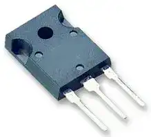
- Transistor Case Style: TO-247
- Drain Source Voltage Vds: 600V
- Operating Temperature Max: 150°C
- Continuous Drain Current Id: 29A
- Drain Source On State Resistance: 0.102ohm
- Gate Source Threshold Voltage Max: 3.5V
| Delivery and price | |
|---|---|
| Units per pack | 1000 |
| Price | 2.0 € |
| Current stock | 10+ |
| Lead time | 30 days |
## **Is Now Part of**

**To learn more about ON Semiconductor, please visit our website at www.onsemi.com**

ON Semiconductor and the ON Semiconductor logo are trademarks of Semiconductor Components Industries, LLC dba ON Semiconductor or its subsidiaries in the United States and/or other countries. ON Semiconductor owns the rights to a number of patents, trademarks, copyrights, trade secrets, and other intellectual property. A listing of ON Semiconductor’s product/patent coverage may be accessed at www.onsemi.com/site/pdf/Patent-Marking.pdf. ON Semiconductor reserves the right to make changes without further notice to any products herein. ON Semiconductor makes no warranty, representation or guarantee regarding the suitability of its products for any particular purpose, nor does ON Semiconductor assume any liability arising out of the application or use of any product or circuit, and specifically disclaims any and all liability, including without limitation special, consequential or incidental damages. Buyer is responsible for its products and applications using ON Semiconductor products, including compliance with all laws, regulations and safety requirements or standards, regardless of any support or applications information provided by ON Semiconductor. “Typical” parameters which may be provided in ON Semiconductor data sheets and/or specifications can and do vary in different applications and actual performance may vary over time. All operating parameters, including “Typicals” must be validated for each customer application by customer’s technical experts. ON Semiconductor does not convey any license under its patent rights nor the rights of others. ON Semiconductor products are not designed, intended, or authorized for use as a critical component in life support systems or any FDA Class 3 medical devices or medical devices with a same or similar classification in a foreign jurisdiction or any devices intended for implantation in the human body. Should Buyer purchase or use ON Semiconductor products for any such unintended or unauthorized application, Buyer shall indemnify and hold ON Semiconductor and its officers, employees, subsidiaries, affiliates, and distributors harmless against all claims, costs, damages, and expenses, and reasonable attorney fees arising out of, directly or indirectly, any claim of personal injury or death associated with such unintended or unauthorized use, even if such claim alleges that ON Semiconductor was negligent regarding the design or manufacture of the part. ON Semiconductor is an Equal Opportunity/Affirmative Action Employer. This literature is subject to all applicable copyright laws and is not for resale in any manner.

**==> picture [68 x 8] intentionally omitted <==**

**----- Start of picture text -----**<br>
November 2015<br>**----- End of picture text -----**<br>


## **FCH125N60E N-Channel SuperFET[® ] II Easy-Drive MOSFET**

## **600 V, 29 A, 125 m** Ω

## **Features**

## **Description**

**==> picture [489 x 572] intentionally omitted <==**

**----- Start of picture text -----**<br>
• 650 V @TJ = 150°C SuperFET [®]  II MOSFET is Fairchild Semiconductor’s brand-new<br>• Typ. RDS(on) = 102 mΩ  charge balance technology for outstanding low on-resistance high voltage super-junction (SJ) MOSFET family that is utilizing<br>• Ultra Low Gate Charge (Typ. Qg = 75 nC) and lower gate charge performance. This technology is tailored<br>• Low Effective Output Capacitance (Typ. Coss(eff) = 258 pF) to minimize conduction loss, provide superior switching performance, dv/dt rate and higher avalanche energy.<br>• 100% Avalanche Tested Consequently, SuperFET II MOSFET easy-drive series offers<br>• RoHS Compliant slightly slower rise and fall times compared to the SuperFET II<br>MOSFET series. Noted by the “E” part number suffix, this family<br>Applications helps manage EMI issues and allows for easier design<br>implementation. For faster switching in applications where<br>• Telecom / Sever Power Supplies switching losses must be at an absolute minimum, please<br>• Industrial Power Supplies consider the SuperFET II MOSFET series.<br>D<br>PP<br>G G<br>D<br>TO-247<br>S<br>S<br>Absolute Maximum Ratings TC = 25oC unless otherwise noted.<br>Symbol Parameter FCH125N60E Unit<br>VDSS Drain to Source Voltage 600 V<br> - DC ±20<br>VGSS Gate to Source Voltage  - AC                                               (f > 1 Hz) ±30 V<br>ID Drain Current  - Continuous  - Continuous ((TTCC = 25 = 100 [o] C [o] C) ) 1829 A<br>IDM Drain Current  - Pulsed                                        (Note 1) 87 A<br>EAS Single Pulsed Avalanche Energy (Note 2) 720 mJ<br>IAR Avalanche Current                                                                                         (Note 1) 6 A<br>EAR Repetitive Avalanche Energy (Note 1) 2.78 mJ<br>MOSFET dv/dt                                                                  100<br>dv/dt V/ns<br>Peak Diode Recovery dv/dt                                                                         (Note 3) 20<br>PD Power Dissipation  - Derate Above 25 (TC = 25 [o] C) [o] C 2782.2 W/W [o] C<br>TJ, TSTG Operating and Storage Temperature Range -55 to +150 oC<br>= TL = [eS] Maximum Lead Temperature for Soldering, 1/8” from Case for 5 Seconds 300 oC<br>Thermal Characteristics<br>Symbol Parameter FCH125N60E Unit<br>RθJC Thermal Resistance, Junction to Case, Max.            0.45 oC/W<br>ee RθJA Thermal Resistance, Junction to Ambient, Max.             40<br>©2015 Fairchild Semiconductor Corporation 1<br>FCH125N60E Rev.1.0<br>**----- End of picture text -----**<br>


www.fairchildsemi.com

## **Package Marking and Ordering Information**

|**Electrical Characteristics**TC= 25oC unless otherwise noted.<br>**Off Characteristics**<br>**On Characteristics**<br>**Dynamic Characteristics**<br>**Part Number**<br>**Top Mark**<br>**Package**<br>**Packing Method**<br>**Reel Size**<br>**Tape Width**<br>**Quantity**<br>FCH125N60E<br>FCH125N60E<br>TO-247<br>Tube<br>N/A<br>N/A<br>30 units<br>**Symbol**<br>**Parameter**<br>**Test Conditions**<br>**Min.**<br>**Typ.**<br>**Max.**<br>**Unit**<br>BVDSS<br>Drain to Source Breakdown Voltage<br>VGS= 0 V, ID= 10 mA, TJ= 25°C<br>600<br>-<br>-<br>V<br>VGS= 0 V, ID= 10 mA, TJ= 150°C<br>650<br>-<br>-<br>V<br>ΔBVDSS<br>/ΔTJ<br>Breakdown Voltage Temperature<br>Coefficient<br>ID= 10 mA, Referenced to 25oC<br>-<br>0.7<br>-<br>V/oC<br>IDSS<br>Zero Gate Voltage Drain Current<br>VDS= 600 V, VGS= 0 V<br>-<br>-<br>1<br>μA<br>VDS= 480 V, VGS= 0 V,TC= 125oC<br>-<br>2<br>-<br>IGSS<br>Gate to BodyLeakage Current<br>VGS= ±20 V, VDS= 0 V<br>-<br>-<br>±100<br>nA<br>VGS(th)<br>Gate Threshold Voltage<br>VGS= VDS, ID= 250μA<br>2.5<br>-<br>3.5<br>V<br>RDS(on)<br>Static Drain to Source On Resistance<br>VGS= 10 V, ID= 14.5 A<br>-<br>102<br>125<br>mΩ<br>gFS<br>Forward Transconductance<br>VDS= 20 V, ID= 14.5 A<br>-<br>25<br>-<br>S<br>Ciss<br>Input Capacitance<br>VDS= 380 V, VGS= 0 V,<br>f = 1 MHz<br>-<br>2250<br>2990<br>pF<br>Coss<br>Output Capacitance<br>-<br>60<br>80<br>pF<br>Crss<br>Reverse Transfer Capacitance<br>-<br>17<br>-<br>pF<br>Coss(eff.)<br>Effective Output Capacitance<br>VDS= 0 V to 480 V, VGS= 0 V<br>-<br>258<br>-<br>pF<br>Qg(tot)<br>Total Gate Charge at 10V<br>VDS= 380 V, ID= 14.5 A,<br>VGS= 10 V<br>(Note  4)<br>-<br>75<br>95<br>nC<br>Qgs<br>Gate to Source Gate Charge<br>-<br>10<br>-<br>nC<br>Qgd<br>Gate to Drain “Miller” Charge<br>-<br>33<br>-<br>nC<br>~~ee~~<br>~~——————————~~|
|---|
|ESR<br>Equivalent Series Resistance<br>f = 1 MHz<br>-<br>3.5<br>-<br>Ω|
|**Switching Characteristics**|
|**Drain-Source Diode Characteristics**<br>td(on)<br>Turn-On DelayTime<br>VDD= 380 V, ID= 14.5 A,<br>VGS= 10 V, Rg= 4.7Ω<br>(Note 4)<br>-<br>23<br>56<br>ns<br>tr<br>Turn-On Rise Time<br>-<br>20<br>50<br>ns<br>td(off)<br>Turn-Off DelayTime<br>-<br>106<br>222<br>ns<br>tf<br>Turn-Off Fall Time<br>-<br>23<br>56<br>ns<br>~~==—~~<br>~~BE~~|
|IS<br>Maximum Continuous Drain to Source Diode Forward Current<br>-<br>-<br>29<br>A<br>ISM<br>Maximum Pulsed Drain to Source Diode Forward Current<br>-<br>-<br>87<br>A<br>VSD<br>Drain to Source Diode Forward Voltage<br>VGS= 0 V, ISD= 14.5 A<br>-<br>-<br>1.2<br>V<br>trr<br>Reverse RecoveryTime<br>VGS= 0 V, ISD= 14.5 A,<br>dIF/dt = 100 A/μs<br>-<br>376<br>-<br>ns<br>Qrr<br>Reverse RecoveryCharge<br>-<br>6.5<br>-<br>μC<br>~~Se~~|


**Notes:**

1. Repetitive rating: pulse width limited by maximum junction temperature.

2. IAS = 6.0 A, RG = 25 Ω, Starting TJ = 25°C

3. ISD ≤ 14.5 A, di/dt ≤ 200 A/μs, VDD ≤ 380 V, Starting TJ = 25°C

4. Essentially independent of operating temperature.

©2015 Fairchild Semiconductor Corporation FCH125N60E Rev. 1.0

www.fairchildsemi.com

**2**

## **Typical Performance Characteristics**

**==> picture [456 x 604] intentionally omitted <==**

**----- Start of picture text -----**<br>
Figure 1. On-Region Characteristics Figure 2. Transfer Characteristics<br>100 100<br>*Notes:<br>   1. VDS = 20V<br>   2. 250 μ s Pulse Test<br>10 10<br>ae V            8.0VGS = 10.0V       Lu 150 o C<br>            7.0V            6.0V 25 o C<br>*Notes:             5.5V<br>   1. 250   2. TC = 25 μ s Pulse Test [o] C             5.0V            4.5V -55oC<br>1 “| 1 LA [|<br>0.3 1 10 2 3 4 5 6 7<br>VDS, Drain-Source Voltage[V] VGS, Gate-Source Voltage[V]<br>Figure 3. On-Resistance Variation vs.  Figure 4. Body Diode Forward Voltage<br>                     Drain Current and Gate Voltage                  Variation vs. Source Current<br>                                                                                                               and Temperature<br>100<br>0.3 *Notes:<br>*Note: TC = 25 [o] C 1. VGS = 0V<br>10 2. 250 μ s Pulse Test<br>0.2  150 [o] C<br>alae 1 TF<br>25 [o] C<br>VGS = 10V 0.1<br>0.1 VGS = 20V -55 o C<br>0.01<br>0.001<br>0.0 HHH 0.0 By 0.3 0.6 EREEEE 0.9 1.2 1.5<br>0 20 40 60 80 100<br>ID, Drain Current [A] VSD, Body Diode Forward Voltage [V]<br>Figure 5. Capacitance Characteristics Figure 6. Gate Charge Characteristics<br>100000 10<br>*Note: ID = 14.5A<br>10000 8 VDS = 120V<br>Ciss<br>1000 SS, FEE VDS = 300V<br>6<br>Coss<br>100 VDS = 480V<br>4<br>*Note:<br>10    1. VGS = 0V<br>   2. f = 1MHz<br>2<br>1 eS C iss  = C gs  + C gd  (C ds  = shorted) Crss<br>Coss = Cds + Cgd<br>0.1 Crss = Cgd 0 Pe<br>-1 2 3 0 16 32 48 64 80<br>10 1 10 10 10<br>ee VDS, Drain-Source Voltage [V] b= Annee Qg, Total Gate Charge [nC]<br>, Drain Current[A] , Drain Current[A]<br>ID ID<br>],<br>Ω<br> [<br>DS(ON)<br>R<br>, Reverse Drain Current [A]<br>IS<br>Drain-Source On-Resistance<br>, Gate-Source Voltage [V]<br>Capacitances [pF] GS<br>V<br>**----- End of picture text -----**<br>


©2015 Fairchild Semiconductor Corporation FCH125N60E Rev. 1.0

www.fairchildsemi.com

**3**

## **Typical Performance Characteristics** (Continued)

**==> picture [457 x 602] intentionally omitted <==**

**----- Start of picture text -----**<br>
       Figure 7. Breakdown Voltage Variation                      Figure 8. On-Resistance Variation<br>                        vs. Temperature                                                            vs. Temperature<br>1.2 2.5<br>*Notes: *Notes:<br>   1. VGS = 0V    1. VGS = 10V<br>   2. ID = 10mA    2. ID = 14.5A<br>1.1 2.0<br>| tty tA<br>1.0 1.5<br>EapaGn feta<br>0.9 1.0<br>“Gun Gavan<br>0.8 0.5<br>-100 PEP -50 0 50 EEE 100 150 200 -100 ty -50 0 50 100 150 200<br>TJ, Junction Temperature [ [o] C] TJ, Junction Temperature [ [o] C]<br>          Figure 9. Maximum Safe Operating Area                   Figure 10. Maximum Drain Current<br>                                                                                                                     vs. Case Temperature<br>100 30<br>10 μ s<br>100 μ s 24<br>10 PN) PERE<br>18<br>cali SE 1ms NSE<br>Operation in This Area  DC<br>is Limited by R DS(on) 12<br>1 *Notes: a TNS<br>TC = 25 [o] C . 6 TN<br>T J  = 150 [o] C<br>R θ JC = 0.45 [o] C/W<br>0.1 i 0 foeen<br>1 10 100 1000 25 50 75 100 125 150<br>VDS, Drain-Source Voltage [V] TC, Case Temperature [ [o] C]<br>   Figure 11. Eoss vs. Drain to Source Voltage<br>15129 EnnaCTT TZ<br>6<br>annp? ae<br>3<br>ir  ane [TT]<br>0 (AGnanEGe<br>0 120 240 360 480 600<br>VDS, Drain to Source Voltage [V]<br>, [Normalized] , [Normalized]<br>DSS DS(on)<br>BV R<br>Drain-Source On-Resistance<br>Drain-Source Breakdown Voltage<br>, Drain Current [A]<br>ID , Drain Current [A]<br>ID<br>J]<br>μ<br>, [<br>OSS<br>E<br>**----- End of picture text -----**<br>


©2015 Fairchild Semiconductor Corporation FCH125N60E Rev. 1.0

www.fairchildsemi.com

**4**

## **Typical Performance Characteristics** (Continued)

**==> picture [300 x 180] intentionally omitted <==**

**----- Start of picture text -----**<br>
1<br>ss<br>0.5<br>0.1 0.2 PDM<br>0.1 t1<br>0.05 t 2<br>*Notes:<br>0.02<br>0.01    1. Z θ JC(t) = 0.45 [o] C/W Max.<br>0.01 Single pulse    2. Duty Factor, D= t1/t2<br>   3. TJM - TC = PDM * Z θ JC(t)<br>0.00510 SS -5 iieecsieeearieease 10-4 10-3 10-2 10-1 1 10<br>t1, Rectangular Pulse Duration [sec]<br>oC/W]Thermal Response [<br>(t),<br>ZJC θ<br>**----- End of picture text -----**<br>


©2015 Fairchild Semiconductor Corporation FCH125N60E Rev. 1.0

www.fairchildsemi.com

**5**

**==> picture [392 x 412] intentionally omitted <==**

**----- Start of picture text -----**<br>
IG = const.<br>a<br>Charge<br> Figure 13. Gate Charge Test Circuit & Waveform<br>VDS RL VDS 90%<br>VGS VDD<br>RG<br>10%<br>V 10V GS DUT VGS<br>td(on) tr td(off) tf<br>te wa t on LS t off<br> Figure 14. Resistive Switching Test Circuit & Waveforms<br>Vos ryA EAS™a“5 Las?“IAS<br>lo on} BVpss<br>oF las<br>: R (ie) =F Voo lo (t)<br>VGS<br>q t DUT Vop<br>**----- End of picture text -----**<br>


**Figure 15. Unclamped Inductive Switching Test Circuit & Waveforms**

©2015 Fairchild Semiconductor Corporation FCH125N60E Rev. 1.0

www.fairchildsemi.com

**6**

**==> picture [305 x 476] intentionally omitted <==**

**----- Start of picture text -----**<br>
DUT +<br>VDS<br>_<br>I SD<br>L<br>Driver<br>RG<br>Same Type<br>as DUT VDD<br>VGS • dv/dt controlled by  RG<br>• ISD controlled by pulse period<br>Gate Pulse Width<br>VGS D = --------------------------Gate Pulse Period 10V<br>( Driver )<br>——<br>IFM , Body Diode Forward Current<br>I SD<br>( DUT ) di/dt<br>IRM<br>4 Nee<br>Body Diode Reverse Current<br>VDS<br>( DUT ) Body Diode Recovery dv/dt<br>VSD VDD<br>TT<br>Body Diode<br>Forward Voltage Drop<br>**----- End of picture text -----**<br>


**Figure 16. Peak Diode Recovery dv/dt Test Circuit & Waveforms**

©2015 Fairchild Semiconductor Corporation FCH125N60E Rev. 1.0

www.fairchildsemi.com

**7**

## **Mechanical Dimensions**

**==> picture [15 x 349] intentionally omitted <==**

**----- Start of picture text -----**<br>
FCH125N60E — N-Channel SuperFET<br>®<br> II Easy-Drive<br>MOSFET<br>**----- End of picture text -----**<br>


## **Figure 17. TO-247, Molded, 3-Lead, Jedec Variation AB**

_Package drawings are provided as a service to customers considering Fairchild components. Drawings may change in any manner without notice. Please note the revision and/or date on the drawing and contact a Fairchild Semiconductor representative to verify or obtain the most recent revision. Package specifications do not expand the terms of Fairchild’s worldwide terms and conditions, specifically the warranty therein, which covers Fairchild products._

_Always visit Fairchild Semiconductor’s online packaging area for the most recent package drawings:_

_http://www.fairchildsemi.com/package/packageDetails.html?id=PN_TO247-003_

©2015 Fairchild Semiconductor Corporation FCH125N60E Rev. 1.0

www.fairchildsemi.com

**8**

## **TRADEMARKS**

The following includes registered and unregistered trademarks and service marks, owned by Fairchild Semiconductor and/or its global subsidiaries, and is not intended to be an exhaustive list of all such trademarks.

AccuPower™ F-PFS™ OPTOPLANAR[®] ®* AttitudeEngine™ FRFET[®] [Ecevent Awinda[®] Global Power Resource[SM] tm[®] AX-CAP[®] * GreenBridge™ Power Supply WebDesigner™ TinyBoost[®] BitSiC™ Green FPS™ PowerTrench[®] TinyBuck[®] Build it Now™ Green FPS™ e-Series™ PowerXS™ TinyCalc™ CorePLUS™ G _max_ ™ Programmable Active Droop™ TinyLogicTINYOPTO™[®] CorePOWER™ GTO™ QFET[®] _CROSSVOLT_ ™ IntelliMAX™ QS™ TinyPower™ CTL™ ISOPLANAR™ Quiet Series™ TinyPWM™ TinyWire™ Current Transfer Logic™DEUXPEED[®] Marking Small Speakers Sound Louder and Better™ RapidConfigure™™ TranSiC™ TriFault Detect™ Dual Cool™ MegaBuck™ o) TRUECURRENT[®] * EcoSPARKEfficentMax™[®] MICROCOUPLER™MicroFET™ Saving our world, 1mW/W/kW at a time™SignalWise™ μSerDes™ ESBC™ MicroPak™ SmartMax™ ® MicroPak2™ SMART START™ MillerDrive™ Solutions for Your Success™ UHC[®] ~~so~~ "WZ... Fairchild[®] MotionMax™ SPM[®] Ultra FRFET™ Fairchild Semiconductor[®] MotionGrid[®] STEALTH™ UniFET™ FACT Quiet Series™ MTi[®] SuperFET[®] VCX™ FACT[®] MTx[®] SuperSOT™-3 VisualMax™ FastvCore™ MVN[®] SuperSOT™-6 VoltagePlus™ FETBench™ mWSaver[®] SuperSOT™-8 XS™ FPS™ OptoHiT™ SupreMOS[®] Xsens™ OPTOLOGIC[®] SyncFET™ 仙童[®] Sync-Lock™

*Trademarks of System General Corporation, used under license by Fairchild Semiconductor.

**DISCLAIMER** FAIRCHILD SEMICONDUCTOR RESERVES THE RIGHT TO MAKE CHANGES WITHOUT FURTHER NOTICE TO ANY PRODUCTS HEREIN TO IMPROVE RELIABILITY, FUNCTION, OR DESIGN. TO OBTAIN THE LATEST, MOST UP-TO-DATE DATASHEET AND PRODUCT INFORMATION, VISIT OUR WEBSITE AT HTTP://WWW.FAIRCHILDSEMI.COM. FAIRCHILD DOES NOT ASSUME ANY LIABILITY ARISING OUT OF THE APPLICATION OR USE OF ANY PRODUCT OR CIRCUIT DESCRIBED HEREIN; NEITHER DOES IT CONVEY ANY LICENSE UNDER ITS PATENT RIGHTS, NOR THE RIGHTS OF OTHERS. THESE SPECIFICATIONS DO NOT EXPAND THE TERMS OF FAIRCHILD’S WORLDWIDE TERMS AND CONDITIONS, SPECIFICALLY THE WARRANTY THEREIN, WHICH COVERS THESE PRODUCTS.

**AUTHORIZED USE** Unless otherwise specified in this data sheet, this product is a standard commercial product and is not intended for use in applications that require extraordinary levels of quality and reliability. This product may not be used in the following applications, unless specifically approved in writing by a Fairchild officer: (1) automotive or other transportation, (2) military/aerospace, (3) any safety critical application – including life critical medical equipment – where the failure of the Fairchild product reasonably would be expected to result in personal injury, death or property damage. Customer’s use of this product is subject to agreement of this Authorized Use policy. In the event of an unauthorized use of Fairchild’s product, Fairchild accepts no liability in the event of product failure. In other respects, this product shall be subject to Fairchild’s Worldwide Terms and Conditions of Sale, unless a separate agreement has been signed by both Parties.

## **ANTI-COUNTERFEITING POLICY**

Fairchild Semiconductor Corporation's Anti-Counterfeiting Policy. Fairchild's Anti-Counterfeiting Policy is also stated on our external website, www.fairchildsemi.com, under Terms of Use Counterfeiting of semiconductor parts is a growing problem in the industry. All manufacturers of semiconductor products are experiencing counterfeiting of their parts. Customers who inadvertently purchase counterfeit parts experience many problems such as loss of brand reputation, substandard performance, failed applications, and increased cost of production and manufacturing delays. Fairchild is taking strong measures to protect ourselves and our customers from the proliferation of counterfeit parts. Fairchild strongly encourages customers to purchase Fairchild parts either directly from Fairchild or from Authorized Fairchild Distributors who are listed by country on our web page cited above. Products customers buy either from Fairchild directly or from Authorized Fairchild Distributors are genuine parts, have full traceability, meet Fairchild’s quality standards for handling and storage and provide access to Fairchild’s full range of up-to-date technical and product information. Fairchild and our Authorized Distributors will stand behind all warranties and will appropriately address and warranty issues that may arise. Fairchild will not provide any warranty coverage or other assistance for parts bought from Unauthorized Sources. Fairchild is committed to combat this global problem and encourage our customers to do their part in stopping this practice by buying direct or from authorized distributors.

## **PRODUCT STATUS DEFINITIONS**

**Definition of Terms**

|**Definition of Terms**|||
|---|---|---|
|**Datasheet Identification**|**Product Status**|**Definition**|
|Advance Information|Formative / In Design|Datasheet contains the design specifications for product development. Specifications<br>may change in any manner without notice.|
|Preliminary|First Production|Datasheet contains preliminary data; supplementary data will be published at a later<br>date. Fairchild Semiconductor reserves the right to make changes at any time without<br>notice to improve design.|
|No Identification Needed|Full Production|Datasheet contains final specifications. Fairchild Semiconductor reserves the right to<br>make changes at any time without notice to improve the design.|
|Obsolete|Not In Production|Datasheet contains specifications on a product that is discontinued by Fairchild<br>Semiconductor. The datasheet is for reference information only.|


Rev. I77

www.fairchildsemi.com

©2015 Fairchild Semiconductor Corporation FCH125N60E Rev. 1.0

**9**

ON Semiconductor and      are trademarks of Semiconductor Components Industries, LLC dba ON Semiconductor or its subsidiaries in the United States and/or other countries. ON Semiconductor owns the rights to a number of patents, trademarks, copyrights, trade secrets, and other intellectual property. A listing of ON Semiconductor’s product/patent coverage may be accessed at www.onsemi.com/site/pdf/Patent−Marking.pdf. ON Semiconductor reserves the right to make changes without further notice to any products herein. ON Semiconductor makes no warranty, representation or guarantee regarding the suitability of its products for any particular purpose, nor does ON Semiconductor assume any liability arising out of the application or use of any product or circuit, and specifically disclaims any and all liability, including without limitation special, consequential or incidental damages. Buyer is responsible for its products and applications using ON Semiconductor products, including compliance with all laws, regulations and safety requirements or standards, regardless of any support or applications information provided by ON Semiconductor. “Typical” parameters which may be provided in ON Semiconductor data sheets and/or specifications can and do vary in different applications and actual performance may vary over time. All operating parameters, including “Typicals” must be validated for each customer application by customer’s technical experts. ON Semiconductor does not convey any license under its patent rights nor the rights of others. ON Semiconductor products are not designed, intended, or authorized for use as a critical component in life support systems or any FDA Class 3 medical devices or medical devices with a same or similar classification in a foreign jurisdiction or any devices intended for implantation in the human body. Should Buyer purchase or use ON Semiconductor products for any such unintended or unauthorized application, Buyer shall indemnify and hold ON Semiconductor and its officers, employees, subsidiaries, affiliates, and distributors harmless against all claims, costs, damages, and expenses, and reasonable attorney fees arising out of, directly or indirectly, any claim of personal injury or death associated with such unintended or unauthorized use, even if such claim alleges that ON Semiconductor was negligent regarding the design or manufacture of the part. ON Semiconductor is an Equal Opportunity/Affirmative Action Employer. This literature is subject to all applicable copyright laws and is not for resale in any manner.

## **PUBLICATION ORDERING INFORMATION**

**N. American Technical Support** : 800−282−9855 Toll Free **ON Semiconductor Website** : **www.onsemi.com** USA/Canada

## **LITERATURE FULFILLMENT** :

Literature Distribution Center for ON Semiconductor

**Order Literature** : http://www.onsemi.com/orderlit For additional information, please contact your local Sales Representative

19521 E. 32nd Pkwy, Aurora, Colorado 80011 USA **Europe, Middle East and Africa Technical Support: Phone** : 303−675−2175 or 800−344−3860 Toll Free USA/Canada Phone: 421 33 790 2910 **Fax** : 303−675−2176 or 800−344−3867 Toll Free USA/Canada **Japan Customer Focus Center Email** : orderlit@onsemi.com Phone: 81−3−5817−1050

© Semiconductor Components Industries, LLC

www.onsemi.com

**www.onsemi.com**

**1**
Updated at February 9, 2023
onsemi is a premier global supplier of intelligent power and sensing technologies, driving disruptive innovations across the automotive, industrial, and cloud infrastructure markets. Recognized for their commitment to sustainability and reliable supply chains, the company accelerates advancements in vehicle electrification, industrial automation, and 5G networks by solving the industry's most complex design challenges. At the core of their portfolio is an industry-leading selection of discrete semiconductors. This extensive range features thousands of high-performance bipolar transistors, single and dual MOSFETs, and a comprehensive array of diodes, including Zener, Schottky, and fast-recovery rectifiers. Engineered for superior thermal performance and energy efficiency, these foundational components are critical for demanding power conversion, switching, and signal conditioning applications. Beyond essential discretes, onsemi provides a robust suite of advanced power management and circuit protection solutions. Their lineup includes intelligent power modules, single IGBTs, and transient voltage suppression (TVS) diodes designed to safeguard sensitive circuitry. Complimented by integrated passive filters, AC/DC LED driver ICs, and specialized sub-2.4GHz RF transceivers, onsemi equips engineers with the scalable, high-quality technologies needed to build a cleaner, smarter, and more connected world.
About Novapart
Novapart is a B2B electronic component broker specialising in stock shortages and cost reduction. We source hard-to-find parts and identify compliant alternatives across a catalogue of 540,000+ components from 500+ manufacturers.
Learn more →Stock Shortage Specialist
When a component is unavailable, discontinued or has an unacceptable lead time, we tap into our network of vetted European and Asian distributors to source what you need — without compromising on quality or traceability.
Request a quote →Compliant Alternatives
We identify pin-to-pin, electrically equivalent substitutes that meet the same certifications (RoHS, AEC-Q100, REACH) as your original specification — validated against datasheets, not just part numbers. Often at a lower cost.
BOM Analysis service →