
Image not available
Illustrative purposes only

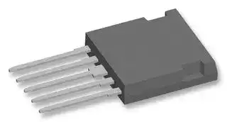
FBE22-06N1
Bridge Rectifier, Single Phase, 600 V, 22 A, i4-Pac, 5 Pins, 2.35 V
⚠️ Reference pricing provided. In case of supply shortages, we will connect you with our trusted procurement partners to ensure your project's continuity.
- Manufacturer: IXYS SEMICONDUCTOR
- Product type: Bridge Rectifier Diodes
- SVHC: No SVHC (12-Jan-2017)
- No. of Pins: 5Pins
- No. of Phases: Single Phase
- Product Range: HiPerFRED Series
- Forward Voltage Max: 2.35V
- Forward Surge Current: 50A
- Average Forward Current: 22A
- Bridge Rectifier Mounting: Through Hole
- Operating Temperature Max: 150°C
- Bridge Rectifier Case Style: i4-Pac
- Repetitive Peak Reverse Voltage: 600V
| Delivery and price | |
|---|---|
| Units per pack | 250 |
| Price | 7.63 € |
| Current stock | 10+ |
| Lead time | 30 days |
Datasheet

**FBE22-06N1**

## **HiPerFRED**

**VRRM** _**=**_ **600 V I DAV** _**=**_ **22 A t rr** _**=**_ **30 ns**

High Performance Fast Recovery Diode Low Loss and Soft Recovery 1~ Rectifier Bridge

## **Part number**

## **FBE22-06N1**

Backside: isolated

**==> picture [158 x 8] intentionally omitted <==**

**----- Start of picture text -----**<br>
2 5 4 1<br>**----- End of picture text -----**<br>


## **Features / Advantages:**

- Planar passivated chips

- Very low leakage current

- Very short recovery time

- Improved thermal behaviour

- Very low Irm-values

- Very soft recovery behaviour

- Avalanche voltage rated for reliable operation

- Soft reverse recovery for low EMI/RFI

## **Applications:**

- Rectifiers in switch mode power supplies (SMPS)

## **Package:** i4-Pac

   - Isolation Voltage:          V~3000

   - Industry convenient outline

   - RoHS compliant

   - Epoxy meets UL 94V-0

   - Soldering pins for PCB mounting

   - Backside: DCB ceramic

   - Reduced weight

   - Advanced power cycling

- Low Irm reduces:

- Power dissipation within the diode

- Turn-on loss in the commutating switch

## **Disclaimer Notice**

Information furnished is believed to be accurate and reliable. However, users should independently evaluate the suitability of and test each product selected for their own applications. Littelfuse products are not designed for, and may not be used in, all applications. Read complete Disclaimer Notice at www.littelfuse.com/disclaimer-electronics.

IXYS reserves the right to change limits, conditions and dimensions.

Data according to IEC 60747and per semiconductor unless otherwise specified

20191211b

© 2019 IXYS all rights reserved

**FBE22-06N1**

|**Fast Diode**|**Fast Diode**|**Ratings**<br>**typ.**<br>**max.**<br>**min.**<br>**Unit**|**Ratings**<br>**typ.**<br>**max.**<br>**min.**<br>**Unit**|**Ratings**<br>**typ.**<br>**max.**<br>**min.**<br>**Unit**|**Ratings**<br>**typ.**<br>**max.**<br>**min.**<br>**Unit**|**Ratings**<br>**typ.**<br>**max.**<br>**min.**<br>**Unit**|
|---|---|---|---|---|---|---|
|**Symbol**<br>**Definition**<br>**Conditions**|||||||
|**VRSM**<br>_max. non-repetitive reverse blocking voltage_||T    =   25°C<br>VJ|||600|V|
|**VRRM**<br>_max. repetitive reverse blocking voltage_||T    =   25°C<br>VJ|||600|V|
|**I R**<br>_reverse current, drain current_|V    =          V<br>R<br>V    =          V<br>R<br>600<br>600|T    =   25°C<br>VJ<br>T    =       °C<br>VJ<br>150|||60<br>0.25|mA<br>µA|
|**VF**<br>_forward voltage drop_|I  =          A<br>F<br>11<br>I  =          A<br>F<br>22|T    =   25°C<br>VJ|||2.13<br>2.35|V<br>V|
||I  =          A<br>F<br>11<br>I  =          A<br>F<br>22|T    =       °C<br>VJ<br>150|||1.44<br>1.71|V<br>V|
|**I**<br>**DAV**<br>_bridge output current_|T  =       °C<br>C<br>115<br>d =<br>rectangular<br>0.5|T    =       °C<br>VJ<br>175|||22|A|
|**VF0**<br>**rF**<br>_threshold voltage_<br>_slope resistance_<br>_for power loss calculation only_||T    =       °C<br>VJ<br>175|||1.04<br>24|V<br>mΩ|
|**R**<br>_thermal resistance junction to case_<br>**thJC**|||||3|K/W|
|**R**<br>_thermal resistance case to heatsink_<br>**thCH**||||0.2||K/W|
|**Ptot**<br>_total power dissipation_||T    =   25°C<br>C|||50|W|
|**IFSM**<br>t = 10 ms; (50 Hz), sine;<br>_max. forward surge current_<br>V  = 0 V<br>R||T    =   45°C<br>VJ|||50|A|
|**CJ**<br>_junction capacitance_<br>V  =         V<br>400<br>f = 1 MHz<br>R||T    =   25°C<br>VJ||6||pF|
|_reverse recovery time_<br>**IRM**<br>_max. reverse recovery current_<br>IF =<br>A;<br>10<br>-diF<br>=<br>A/µs<br>200<br>/dt<br>**trr**<br>VR =<br>V<br>300||TVJ =<br>°C<br>25<br>T<br>=<br>100°C<br>VJ||3.5<br>6||A<br>A|
|||TVJ =<br>°C<br>25<br>T<br>=<br>100°C<br>VJ||30<br>90||ns<br>ns|


IXYS reserves the right to change limits, conditions and dimensions.

Data according to IEC 60747and per semiconductor unless otherwise specified

20191211b

© 2019 IXYS all rights reserved

**FBE22-06N1**

|**Ratings**<br>**Package**<br>**i4-Pac**|**Ratings**<br>**Package**<br>**i4-Pac**|**Ratings**<br>**Package**<br>**i4-Pac**|**Ratings**<br>**Package**<br>**i4-Pac**|**Ratings**<br>**Package**<br>**i4-Pac**|
|---|---|---|---|---|
|**Symbol**<br>**Definition**<br>**Conditions**|**min.**|**typ.**|**max.**|**Unit**|
|**I RMS**<br>_RMS current_<br>per terminal|||35|A|
|**TVJ**<br>_virtual junction temperature_|-55||175|°C|
|**Top**<br>_operation temperature_|-55||150|°C|
|**Tstg**<br>_storage temperature_|-55||150|°C|
|**Weight**||9||g|
|**FC**<br>_mounting force with clip_|20||120|N|
|**dSpp/App**<br>_creepage distance on surface | striking distance through air_<br>**dSpb/Apb**<br>_terminal to backside_<br>_terminal to terminal_|1.7|||mm<br>mm|
||5.1||||
|**V**<br>t = 1 second<br>t = 1 minute<br>_isolation voltage_<br>50/60 Hz, RMS; I≤1 mA<br>ISOL<br>**ISOL**|3000||V<br>V||
||2500||||


**==> picture [192 x 144] intentionally omitted <==**

**----- Start of picture text -----**<br>
Product Marking<br>UL<br>Logo IXYS ®<br>ISOPLUS®<br>Part Number XXXXXXXXX<br>Date Code yywwZ 1234<br>Location<br>Lot#<br>**----- End of picture text -----**<br>


**==> picture [215 x 78] intentionally omitted <==**

|**rdering**|**Ordering Number**|**Marking on Product**|**Delivery Mode**|**Quantity**|**Code No.**|
|---|---|---|---|---|---|
|tandard|FBE22-06N1|FBE22-06N1|Tube|25|484954|


**==> picture [341 x 68] intentionally omitted <==**

**----- Start of picture text -----**<br>
 Equivalent Circuits for Simulation * on die level T    =VJ 175°C<br>I V0 R 0 Fast<br>Diode<br>V 0 max threshold voltage 1.04 V<br>R0 max slope resistance * 21 mΩ<br>**----- End of picture text -----**<br>


IXYS reserves the right to change limits, conditions and dimensions.

Data according to IEC 60747and per semiconductor unless otherwise specified

20191211b

© 2019 IXYS all rights reserved

**FBE22-06N1**

## **Outlines i4-Pac**

||||b4<br>4x e<br>E<br>W<br>A<br>A2<br>A1<br>c<br>4x b2<br>5x b<br>E1<br>D1<br>D2<br>Q<br>**2**<br>**5**<br>**3**<br>**4**<br>D3<br>Die konvexe Form des Substrates ist typ. < 0.05 mm über<br>der Kunststoffoberflächeder Bauteilunterseite<br>_The convexbow of substrate is typ. < 0.05 mmover plastic_<br>_surface level ofdevice bottom side_<br>min<br>max<br>min<br>max<br>4.83<br>5.21<br>0.190<br>0.205<br>2.59<br>3.00<br>0.102<br>0.118<br>1.17<br>2.16<br>0.046<br>0.085<br>1.14<br>1.40<br>0.045<br>0.055<br>1.47<br>1.73<br>0.058<br>0.068<br>2.54<br>2.79<br>0.100<br>0.110<br>0.51<br>0.74<br>0.020<br>0.029<br>0.80<br>21.34<br>0.819<br>0.840<br>4.99<br>15.75<br>0.590<br>0.620<br>1.65<br>2.03<br>0.065<br>0.080<br>0.30<br>20.70<br>0.799<br>0.815<br>9.56<br>20.29<br>0.770<br>0.799<br>6.76<br>17.53<br>0.660<br>0.690<br>3.81 BSC<br>0.150 BSC<br>9.81<br>21.34<br>0.780<br>0.840<br>2.11<br>2.59<br>0.083<br>0.102<br>5.33<br>6.20<br>0.210<br>0.244<br>2.54<br>4.57<br>0.100<br>0.180<br>-<br>0.10<br>-<br>0.004<br>Millimeter<br>Inches|b4<br>4x e<br>E<br>W<br>A<br>A2<br>A1<br>c<br>4x b2<br>5x b<br>E1<br>D1<br>D2<br>Q<br>**2**<br>**5**<br>**3**<br>**4**<br>D3<br>Die konvexe Form des Substrates ist typ. < 0.05 mm über<br>der Kunststoffoberflächeder Bauteilunterseite<br>_The convexbow of substrate is typ. < 0.05 mmover plastic_<br>_surface level ofdevice bottom side_<br>min<br>max<br>min<br>max<br>4.83<br>5.21<br>0.190<br>0.205<br>2.59<br>3.00<br>0.102<br>0.118<br>1.17<br>2.16<br>0.046<br>0.085<br>1.14<br>1.40<br>0.045<br>0.055<br>1.47<br>1.73<br>0.058<br>0.068<br>2.54<br>2.79<br>0.100<br>0.110<br>0.51<br>0.74<br>0.020<br>0.029<br>0.80<br>21.34<br>0.819<br>0.840<br>4.99<br>15.75<br>0.590<br>0.620<br>1.65<br>2.03<br>0.065<br>0.080<br>0.30<br>20.70<br>0.799<br>0.815<br>9.56<br>20.29<br>0.770<br>0.799<br>6.76<br>17.53<br>0.660<br>0.690<br>3.81 BSC<br>0.150 BSC<br>9.81<br>21.34<br>0.780<br>0.840<br>2.11<br>2.59<br>0.083<br>0.102<br>5.33<br>6.20<br>0.210<br>0.244<br>2.54<br>4.57<br>0.100<br>0.180<br>-<br>0.10<br>-<br>0.004<br>Millimeter<br>Inches|b4<br>4x e<br>E<br>W<br>A<br>A2<br>A1<br>c<br>4x b2<br>5x b<br>E1<br>D1<br>D2<br>Q<br>**2**<br>**5**<br>**3**<br>**4**<br>D3<br>Die konvexe Form des Substrates ist typ. < 0.05 mm über<br>der Kunststoffoberflächeder Bauteilunterseite<br>_The convexbow of substrate is typ. < 0.05 mmover plastic_<br>_surface level ofdevice bottom side_<br>min<br>max<br>min<br>max<br>4.83<br>5.21<br>0.190<br>0.205<br>2.59<br>3.00<br>0.102<br>0.118<br>1.17<br>2.16<br>0.046<br>0.085<br>1.14<br>1.40<br>0.045<br>0.055<br>1.47<br>1.73<br>0.058<br>0.068<br>2.54<br>2.79<br>0.100<br>0.110<br>0.51<br>0.74<br>0.020<br>0.029<br>0.80<br>21.34<br>0.819<br>0.840<br>4.99<br>15.75<br>0.590<br>0.620<br>1.65<br>2.03<br>0.065<br>0.080<br>0.30<br>20.70<br>0.799<br>0.815<br>9.56<br>20.29<br>0.770<br>0.799<br>6.76<br>17.53<br>0.660<br>0.690<br>3.81 BSC<br>0.150 BSC<br>9.81<br>21.34<br>0.780<br>0.840<br>2.11<br>2.59<br>0.083<br>0.102<br>5.33<br>6.20<br>0.210<br>0.244<br>2.54<br>4.57<br>0.100<br>0.180<br>-<br>0.10<br>-<br>0.004<br>Millimeter<br>Inches|b4<br>4x e<br>E<br>W<br>A<br>A2<br>A1<br>c<br>4x b2<br>5x b<br>E1<br>D1<br>D2<br>Q<br>**2**<br>**5**<br>**3**<br>**4**<br>D3<br>Die konvexe Form des Substrates ist typ. < 0.05 mm über<br>der Kunststoffoberflächeder Bauteilunterseite<br>_The convexbow of substrate is typ. < 0.05 mmover plastic_<br>_surface level ofdevice bottom side_<br>min<br>max<br>min<br>max<br>4.83<br>5.21<br>0.190<br>0.205<br>2.59<br>3.00<br>0.102<br>0.118<br>1.17<br>2.16<br>0.046<br>0.085<br>1.14<br>1.40<br>0.045<br>0.055<br>1.47<br>1.73<br>0.058<br>0.068<br>2.54<br>2.79<br>0.100<br>0.110<br>0.51<br>0.74<br>0.020<br>0.029<br>0.80<br>21.34<br>0.819<br>0.840<br>4.99<br>15.75<br>0.590<br>0.620<br>1.65<br>2.03<br>0.065<br>0.080<br>0.30<br>20.70<br>0.799<br>0.815<br>9.56<br>20.29<br>0.770<br>0.799<br>6.76<br>17.53<br>0.660<br>0.690<br>3.81 BSC<br>0.150 BSC<br>9.81<br>21.34<br>0.780<br>0.840<br>2.11<br>2.59<br>0.083<br>0.102<br>5.33<br>6.20<br>0.210<br>0.244<br>2.54<br>4.57<br>0.100<br>0.180<br>-<br>0.10<br>-<br>0.004<br>Millimeter<br>Inches|b4<br>4x e<br>E<br>W<br>A<br>A2<br>A1<br>c<br>4x b2<br>5x b<br>E1<br>D1<br>D2<br>Q<br>**2**<br>**5**<br>**3**<br>**4**<br>D3<br>Die konvexe Form des Substrates ist typ. < 0.05 mm über<br>der Kunststoffoberflächeder Bauteilunterseite<br>_The convexbow of substrate is typ. < 0.05 mmover plastic_<br>_surface level ofdevice bottom side_<br>min<br>max<br>min<br>max<br>4.83<br>5.21<br>0.190<br>0.205<br>2.59<br>3.00<br>0.102<br>0.118<br>1.17<br>2.16<br>0.046<br>0.085<br>1.14<br>1.40<br>0.045<br>0.055<br>1.47<br>1.73<br>0.058<br>0.068<br>2.54<br>2.79<br>0.100<br>0.110<br>0.51<br>0.74<br>0.020<br>0.029<br>0.80<br>21.34<br>0.819<br>0.840<br>4.99<br>15.75<br>0.590<br>0.620<br>1.65<br>2.03<br>0.065<br>0.080<br>0.30<br>20.70<br>0.799<br>0.815<br>9.56<br>20.29<br>0.770<br>0.799<br>6.76<br>17.53<br>0.660<br>0.690<br>3.81 BSC<br>0.150 BSC<br>9.81<br>21.34<br>0.780<br>0.840<br>2.11<br>2.59<br>0.083<br>0.102<br>5.33<br>6.20<br>0.210<br>0.244<br>2.54<br>4.57<br>0.100<br>0.180<br>-<br>0.10<br>-<br>0.004<br>Millimeter<br>Inches|b4<br>4x e<br>E<br>W<br>A<br>A2<br>A1<br>c<br>4x b2<br>5x b<br>E1<br>D1<br>D2<br>Q<br>**2**<br>**5**<br>**3**<br>**4**<br>D3<br>Die konvexe Form des Substrates ist typ. < 0.05 mm über<br>der Kunststoffoberflächeder Bauteilunterseite<br>_The convexbow of substrate is typ. < 0.05 mmover plastic_<br>_surface level ofdevice bottom side_<br>min<br>max<br>min<br>max<br>4.83<br>5.21<br>0.190<br>0.205<br>2.59<br>3.00<br>0.102<br>0.118<br>1.17<br>2.16<br>0.046<br>0.085<br>1.14<br>1.40<br>0.045<br>0.055<br>1.47<br>1.73<br>0.058<br>0.068<br>2.54<br>2.79<br>0.100<br>0.110<br>0.51<br>0.74<br>0.020<br>0.029<br>0.80<br>21.34<br>0.819<br>0.840<br>4.99<br>15.75<br>0.590<br>0.620<br>1.65<br>2.03<br>0.065<br>0.080<br>0.30<br>20.70<br>0.799<br>0.815<br>9.56<br>20.29<br>0.770<br>0.799<br>6.76<br>17.53<br>0.660<br>0.690<br>3.81 BSC<br>0.150 BSC<br>9.81<br>21.34<br>0.780<br>0.840<br>2.11<br>2.59<br>0.083<br>0.102<br>5.33<br>6.20<br>0.210<br>0.244<br>2.54<br>4.57<br>0.100<br>0.180<br>-<br>0.10<br>-<br>0.004<br>Millimeter<br>Inches|b4<br>4x e<br>E<br>W<br>A<br>A2<br>A1<br>c<br>4x b2<br>5x b<br>E1<br>D1<br>D2<br>Q<br>**2**<br>**5**<br>**3**<br>**4**<br>D3<br>Die konvexe Form des Substrates ist typ. < 0.05 mm über<br>der Kunststoffoberflächeder Bauteilunterseite<br>_The convexbow of substrate is typ. < 0.05 mmover plastic_<br>_surface level ofdevice bottom side_<br>min<br>max<br>min<br>max<br>4.83<br>5.21<br>0.190<br>0.205<br>2.59<br>3.00<br>0.102<br>0.118<br>1.17<br>2.16<br>0.046<br>0.085<br>1.14<br>1.40<br>0.045<br>0.055<br>1.47<br>1.73<br>0.058<br>0.068<br>2.54<br>2.79<br>0.100<br>0.110<br>0.51<br>0.74<br>0.020<br>0.029<br>0.80<br>21.34<br>0.819<br>0.840<br>4.99<br>15.75<br>0.590<br>0.620<br>1.65<br>2.03<br>0.065<br>0.080<br>0.30<br>20.70<br>0.799<br>0.815<br>9.56<br>20.29<br>0.770<br>0.799<br>6.76<br>17.53<br>0.660<br>0.690<br>3.81 BSC<br>0.150 BSC<br>9.81<br>21.34<br>0.780<br>0.840<br>2.11<br>2.59<br>0.083<br>0.102<br>5.33<br>6.20<br>0.210<br>0.244<br>2.54<br>4.57<br>0.100<br>0.180<br>-<br>0.10<br>-<br>0.004<br>Millimeter<br>Inches|
|---|---|---|---|---|---|---|---|---|---|
||||E|||||||
|D<br>|R|||||Q||||
|||||||||||
|L|L1|||||||||
||**1**|||||||||
||Dim.||Millimeter||Inches|||||
||||min|max|min||max|||
||A<br>||4.83|5.21|0.190||0.205|||
||A1<br>||2.59|3.00|0.102||0.118|||
||A2<br>||1.17|2.16|0.046||0.085|||
||b<br>||1.14|1.40|0.045||0.055|||
||b2<br>||1.47|1.73|0.058||0.068|||
||b4<br>||2.54|2.79|0.100||0.110|||
||c<br>||0.51|0.74|0.020||0.029|||
||D<br>2||0.80<br>|21.34|0.819||0.840|||
||D1<br>1||4.99<br>|15.75|0.590||0.620|||
||D2<br>||1.65|2.03|0.065||0.080|||
||D3<br>2||0.30<br>|20.70|0.799||0.815|||
||E<br>1||9.56<br>|20.29|0.770||0.799|||
||E1<br>1||6.76<br>|17.53|0.660||0.690|||
||e||3.81 BSC||0.150 BSC|||||
||L<br>1||9.81<br>|21.34|0.780||0.840|||
||L1<br>||2.11|2.59|0.083||0.102|||
||Q<br>||5.33|6.20|0.210||0.244|||
||R<br>||2.54|4.57|0.100||0.180|||
||W||-|0.10|-||0.004|||
|||||||||||
||||2<br>5<br>1<br>4|||||||


IXYS reserves the right to change limits, conditions and dimensions.

Data according to IEC 60747and per semiconductor unless otherwise specified

20191211b

© 2019 IXYS all rights reserved

**FBE22-06N1**

## **Fast Diode**

**==> picture [508 x 660] intentionally omitted <==**

**----- Start of picture text -----**<br>
30 1.4 40<br>25 1.2 TVVJR = 100°C= 300 V TVVJR = 100°C= 300 V<br>T VJ = 150°C 1.0 30<br>20 T VJ = 100°C IF = 20 A<br>IF TVJ = 25 ° C 0.8 IF = 20 A IRM IF = 10 A<br>15 Qr IF = 10 A 20 I F  =  5 A<br>[A] 0.6 I F  = 5 A [A]<br>10 [μC]<br>0.4<br>10<br>5<br>0.2<br>0 0.0 0<br>0.0 0.5 1.0 1.5 2.0 2.5 100 1000 0 200 400 600 800 1000<br>VF [V] -diF [/dt] [[A/μs]] -diF /dt [A/μs]<br>Fig. 1 Forward current Fig. 2  Typ. reverse recov. charge Fig. 3 Typ. peak reverse current<br>IF versus VF Qr versus -diF /dt IRM versus -diF /dt<br>2.0 120 20 1.2<br>110 TVVJR = 100°C= 300 V TVJ IF= 100°C= 10 A<br>1.5 15 0.9<br>100 I F = 20 A<br>Kf 1.0 trr 90 IIFF = 10 A = 5 A VFR10 0.6tfr<br>[V] [μs]<br>[ns]<br>IRM 80<br>0.5 5 0.3<br>VFR trr<br>Qr 70<br>0.0 0 0.0<br>0 40 80 120 160 0 200 400 600 800 1000 0 200 400 600 800 1000<br>TVJ [°C] -diF /dt [A/μs] -diF [/dt] [[A/μs]]<br>Fig. 4 Dynamic parameters Fig. 5 Typ. recovery time Fig. 6 Typ. peak forward voltage<br>Qr, IRM versus TVJ trr versus -diF /dt VFR and tfr versus diF /dt<br>10<br>Constants for ZthJC calculation:<br>1 i Rthi [K/W] ti [s]<br>ZthJC 1 1.3590 0.1015<br>2 0.4651 0.1026<br>[K/W] 3 0.8473 0.4919<br>0.1 4 0.8473 0.6200<br>0.01<br>1 10 100 1000 10000<br>t [ms]<br>Fig. 7 Transient thermal impedance junction to case<br>**----- End of picture text -----**<br>


IXYS reserves the right to change limits, conditions and dimensions.

Data according to IEC 60747and per semiconductor unless otherwise specified

20191211b

© 2019 IXYS all rights reserved
Updated at June 4, 2026
About Novapart
Novapart is a B2B electronic component broker specialising in stock shortages and cost reduction. We source hard-to-find parts and identify compliant alternatives across a catalogue of 410,000+ components from 500+ manufacturers.
Learn more →Stock Shortage Specialist
When a component is unavailable, discontinued or has an unacceptable lead time, we tap into our network of vetted European and Asian distributors to source what you need — without compromising on quality or traceability.
Request a quote →Compliant Alternatives
We identify pin-to-pin, electrically equivalent substitutes that meet the same certifications (RoHS, AEC-Q100, REACH) as your original specification — validated against datasheets, not just part numbers. Often at a lower cost.
BOM Analysis service →