


EZAST61AAAJ
RC NETWORK, SMD 1608, 1000R, 22PF
- Manufacturer: PANASONIC
- Product type:
- Capacitance:22pF; Filter Type:EMI, RFI; Current Rating:-; Filter Terminals:SMD; Inductance Min:-; Leakage Current Max:-; SVHC:No SVHC (07-Jul-2017); Bleed Resistor Resistance:1kohm
- Product Range: EZAST Series
- Current Rating: -
| Delivery and price | |
|---|---|
| Units per pack | 4000 |
| Price | 0.214 € |
| Current stock | 10+ |
| Lead time | 30 days |
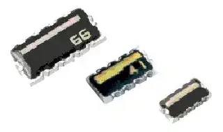
Chip RC Networks

## **Chip RC Networks**

## Type: **EZACT**

## Type: **EZASTB/SSB**

## **EZADT EZAST/SS EZANT**

**==> picture [143 x 7] intentionally omitted <==**

**----- Start of picture text -----**<br>
GND GND<br>**----- End of picture text -----**<br>


**==> picture [110 x 8] intentionally omitted <==**

**----- Start of picture text -----**<br>
GND GND<br>**----- End of picture text -----**<br>


## ■ Features

Smallest SMD R/C networks

- 4 popular noise reduction circuits made

- EZACT : 2.0 mm 1.2 mm 0.6 mm, 0.5 mm pitch (Flat terminal type) EZADT : 3.2 mm 1.6 mm 0.65 mm, 0.635 mm pitch (Concave terminal type) EZAST/SS : 4.0 mm 2.1 mm 0.65 mm, 0.8 mm pitch (Concave terminal type) EZASTB/SSB : 4.0 mm 2.1 mm 0.65 mm, 0.65 mm pitch (Convex terminal type) EZANT : 6.4 mm 3.1 mm 0.80 mm, 1.27 mm pitch (Concave terminal type)

- Takes up less space than discrete chip resistor & chip capacitor EZACT:25 % of 0402 inches (1.0 mm 0.5 mm) chips placing area EZADT:50 % of 0402 inches (1.0 mm 0.5 mm) chips placing area EZAST/SS, EZASTB/SSB:70 % of 0402 inches (1.0 mm 0.5 mm) chips placing area EZANT:55 % of 0805 inches (2.0 mm 1.2 mm) chips placing area

●RoHS compliant

<Effect of high density placing, PWB space saving>

**==> picture [496 x 259] intentionally omitted <==**

**----- Start of picture text -----**<br>
RC Low pass fi lter AC Terminator<br>I/O I/O I/O I/O<br>a HA A Bel litre]<br>Chip RC Network<br>(EZACT, EZADT, EZAST/SS, EZANT)<br>I/O I/O I/O I/O Chip RC Network<br>(EZACT, EZADT, EZAST/SS, EZANT)<br>ifii 6@] .<br>Discrete Chips<br>I/O I/O Discrete Chips I/O I/O<br>anor<br>eae<br>Chip RC Network<br>(EZASTB/SSB) lsli[il l e)]<br>Chip RC Network<br>(EZASTB/SSB)<br>**----- End of picture text -----**<br>


## ■ Recommended Applications

- Digital equipment such as PCs, printers, HDD, PCMCIA cards, PDAs, and word processors

- Communication equipment, digital cordless phones, automobile phones, GSM, PHS, DECT

- Digital audio and video equipment

- Electronic musical instruments, and other digital devices

Design and specifi cations are each subject to change without notice.  Ask factory for the current technical specifi cations before purchase and/or use. Should a safety concern arise regarding this product, please be sure to contact us immediately.

00 Sep. 2010

– 261 –

Chip RC Networks

## ■ Explanation of Part Numbers

- EZACT[•] EZADT[•] EZAST[•] EZANT (R/C Standard Combination)

**==> picture [463 x 154] intentionally omitted <==**

**----- Start of picture text -----**<br>
1 2 3 4 5 6 7 8 9 10 11 12<br>E Z A S T 3 3 A A A J<br>Common Code Dimension and R/C Standard Combination Design Resistance Suffix for Special<br>Circuit Configuration Configuration Tolerance Requirement<br>Thick Film NoiseSuppression and CT 2.0 mm�1.2 mm Resistance ValueConfiguration ✽1 Capacitance ValueConfiguration ✽2 AAA Standard J ±5 %<br>3.2 mm<br>FilteringComponents DT �1.6 mm Chip RC 01 1022 � � 01 10 pF22 pF<br>ST 4.0 mm�2.1 mm Networks 2 47 � 2 47 pF<br>3 100 � 3 100 pF<br>NT 6.4 mm 4 220 � 4 220 pF<br>�3.1 mm<br>5 470 � 5 470 pF<br>6 1 k � 6 1000 pF<br>**----- End of picture text -----**<br>


- ✽1 22 � to 1 k� available for EZADT, EZAST, and EZANT

- ✽2 10 pF and 22 pF available for EZACT. 22 pF to 100 pF available for EZAST, EZADT. 220 pF to 1000 pF available for EZANT.

## ● EZACT[•] EZADT[•] EZASS[•] EZANT (R/C Except the standard Combination)

**==> picture [440 x 176] intentionally omitted <==**

**----- Start of picture text -----**<br>
1 2 3 4 5 6 7 8 9 10 11 12<br>E Z A S S 7 0 1 Y A J<br>Common Code Dimension and Design Number Resistance Suffix for Special<br>Circuit Configuration Tolerance Requirement<br>Thick Film NoiseSuppression and CT 2.0 mm�1.2 mm CT Resistance Value : 10Capacitance Value : 10 pF to 33 pFIn above-mentioned range, it is possible to � to 100 k� J ±5 %<br>Filtering DT 3.2 mm choose optional R/C.<br>Components �1.6 mm Chip RC Resistance Value : 10 � to 100 k�<br>4.0 mm Networks DT Capacitance Value : 10 pF to 100 pF<br>SS In above-mentioned range, it is possible to<br>�2.1 mm choose optional R/C.<br>6.4 mm Resistance Value : 10 � to 100 k�<br>NT �3.1 mm SS Capacitance Value : 10 pF to 180 pFIn above-mentioned range, it is possible to<br>choose optional R/C.<br>Resistance Value : 10 � to 100 k�<br>NT Capacitance Value : 220 pF to 1000 pFIn above-mentioned range, it is possible to<br>choose optional R/C.<br>**----- End of picture text -----**<br>


## ● EZASTB (R/C Standard Combination)

**==> picture [464 x 278] intentionally omitted <==**

**----- Start of picture text -----**<br>
1 2 3 4 5 6 7 8 9 10 11 12<br>E Z A S T B 3 3 A A J<br>Common Code Dimension and R/C Standard Combination Design Resistance Suffix for Special<br>Circuit Configuration Configuration Tolerance Requirement<br>Thick Film Noise Convex Resistance Value Capacitance Value AA Standard J ±5 %<br>Suppression and 4.0 mm terminal type Configuration Configuration<br>STB<br>Filtering �2.1 mm Chip RC 1 22 � 1 22 pF<br>Components Networks 2 47 � 2 47 pF<br>3 100 � 3 100 pF<br>4 220 �<br>5 470 �<br>6 1 k �<br> EZASSB (R/C Except the standard Com bi na tion)<br>1 2 3 4 5 6 7 8 9 10 11 12<br>E Z A S S B 7 0 1 A J<br>Common Code Dimension and Design Number Resistance Suffix for Special<br>Circuit Configuration Tolerance Requirement<br>Thick Film Noise Convex Resistance Value : 10 � to 100 k� J ±5 %<br>Suppression and 4.0 mm terminal type Capacitance Value : 10 pF to 180 pF<br>SSB<br>Filtering �2.1 mm Chip RC In above-mentioned range, it is possible to<br>Components Networks choose optional R/C.<br>**----- End of picture text -----**<br>


## ● EZASSB (R/C Except the standard Com bi na tion)

Design and specifi cations are each subject to change without notice.  Ask factory for the current technical specifi cations before purchase and/or use. Should a safety concern arise regarding this product, please be sure to contact us immediately.

00 Sep. 2010

– 262 –

Chip RC Networks

## ■ Construction

**==> picture [493 x 261] intentionally omitted <==**

**----- Start of picture text -----**<br>
EZACT EZADT EZAST/SS<br>Marking Alumina substrate Marking Alumina substrate Marking<br>Protective coating Alumina substrate GND<br>GND Electrode<br>Electrode (Outer) 33<br>(Outer)<br>GND GND GND<br>Electrode Electrode Electrode<br>Electrode (Outer) Protective coating Electrode (Outer) Protective coating Electrode (Outer)<br>(Outer) (Outer) (Outer)<br>EZANT EZASTB/SSB<br>Marking Alumina substrate<br>Alumina substrate Marking<br>GND GND<br>Electrode Electrode<br>(Outer) G ND (Outer) 33<br>Electrode GND<br>(Outer) Electrode<br>(Outer)<br>Protective coating Electrode Protective coating Electrode<br>(Outer)<br>(Outer)<br>**----- End of picture text -----**<br>


## ■ Circuit Confi guration

**==> picture [493 x 132] intentionally omitted <==**

**----- Start of picture text -----**<br>
EZACT EZADT [•] EZAST/SS [•] EZANT EZASTB/SSB<br>10 9 8 7 10 9 8 7 12 11 10 9 8 7<br>R1 R2 R3 R4 R1 R2 R3 R4 R1 R2 R3 R4<br>GND 1 6 GND GND 1 6 GND<br>C1 C2 C3 C4 C1 C2 C3 C4<br>C1 C2 C3 C4<br>2 3 4 5 2 3 4 5 1 2 3 4 5 6<br>R1=R2=R3=R4 R1=R2=R3=R4 GND R1=R2=R3=R4 GND<br>C1=C2=C3=C4 C1=C2=C3=C4 C1=C2=C3=C4<br>**----- End of picture text -----**<br>


Design and specifi cations are each subject to change without notice.  Ask factory for the current technical specifi cations before purchase and/or use. Should a safety concern arise regarding this product, please be sure to contact us immediately.

00 Sep. 2010

– 263 –

Chip RC Networks

## ■ Dimensions in mm(not to scale)

**==> picture [493 x 692] intentionally omitted <==**

**----- Start of picture text -----**<br>
EZACT EZADT<br>0.33±0.10<br>10 9 8 7<br>10 9 8 7<br>1 6<br>1 6<br>2 3 4 5 (0.635) 2 3 4 5<br>(0.5) 3.20±0.15 0.65+–0.200.10<br>2.0±0.1 0.55±0.10<br>0.20±0.15 0.30±0.15 0.35±0.15 0.35±0.10<br>                                                  Size : 0805 inches                                                   Size : 1206 inches<br>(   ) Reference                         Mass (Weight) [1000 pcs.] :4 g (   ) Reference                         Mass (Weight) [1000 pcs.] :11 g<br>EZAST/SS EZANT<br>0.5±0.2<br>10 9 8 7 10 9 8 7<br>1 6<br>1 33 6<br>2 3 4 5<br>2 3 4 5 (1.27) 0.65±0.20<br>(0.8)<br>4.0±0.2 0.65+– [0.20] 0.10 6.4±0.2 0.80 [+] – [0.20] 0.10<br>0.4±0.2 0.45±0.20 0.5±0.2 0.75±0.20<br>                                                  Size : 1608 inches                                                   Size : 2512 inches<br>(   ) Reference                         Mass (Weight) [1000 pcs.] :17 g (   ) Reference                         Mass (Weight) [1000 pcs.] :55 g<br>EZASTB/SSB<br>0.58±0.2 0.4±0.2 0.25±0.15<br>12 11 10 9 8 7<br>33<br>1 2 3 4 5 6<br>(0.65)<br>4.0±0.2 0.65+– [0.20] 0.10<br>0.275+– [0.200] 0.100 0.2+– [0.2] 0.1<br>                                                  Size : 1608 inches<br>(   ) Reference                         Mass (Weight) [1000 pcs.] :18 g<br>0.10 0.15± 0.1± 0.15±<br>± 0.40 0.2 1.60<br>1.25<br>0.15± 0.15 0.15± 0.15±<br>0.40 ± 0.45 0.40<br>0.25<br>0.2 0.20± 0.2 0.2± 0.20± 0.2±<br>0.5± 0.25 2.1± 0.8 0.25 3.1<br>0.2 0.2± 0.2± 0.20±<br>0.5± 0.4 0.9 0.55<br>0.2<br>± 0.2<br>0.3 ±<br>2.2<br>0.20<br>±<br>0.35<br>**----- End of picture text -----**<br>


Design and specifi cations are each subject to change without notice.  Ask factory for the current technical specifi cations before purchase and/or use. Should a safety concern arise regarding this product, please be sure to contact us immediately.

00 Sep. 2010

– 264 –

Chip RC Networks

## ■ Ratings

||Item|Specif cation|
|---|---|---|
|||10�to 100 k�|
||Resistance Values|EZAC Standard : 10�, 22�, 47�, 100�, 220�, 470�, 1 k�|
|Resistor|Resistance Tolerance<br>Temperature Coeff cient of Resistance (T.C.R.)<br>Rated Power|EZAD/S/N Standard : 22�, 47�, 100�, 220�, 470�, 1 k�<br>±5 %<br>±200�10–6/°C<br>EZAC : 0.031 W(<70 °C(1))<br>EZAD/S/N : 0.063 W(<70 °C(1))|
||Limiting Element Voltage|25 V(2)|
|||EZAC : 10 pF to 33 pF|
|||Standard : 10 pF, 22 pF|
||Capacitance Values<br>(25 °C, 1 kHz(3), 1 Vrms)|EZAD : 10 pF to 100 pF<br>EZAS : 10 pF to 180 pF<br>Standard : 22 pF, 47 pF, 100 pF|
|Capacitor|Capacitance Tolerance<br>Capacitance Temperature Characteristics<br>Dissipation Factor|EZAN : 220 pF to 1000 pF<br>Standard : 220 pF, 470 pF, 1000 pF<br>+30 %/–20 %<br>E Characteristic: +20 %/–55 %(–25 to +85 °C)<br>Less than 3 %(25, 1 kHz(3), 1 Vrms)|
|||EZAC, EZAD : 12 V|
||Rated Voltage|EZAS : 25 V|
|||EZAN : 50 V|
||Category Temperature Range|–25 °C to +85 °C|


(1)  For resistors operated in ambient temperature above 70 °C, rated power shall be derated. (“Power Derating Curve” is shown below)

(2)  Rated Voltage for resistor shall be determined from �Rated Power�Resistance Value, or Limiting Element Voltage whichever less.

(3)  In measuring at 1 MHz, Capacitance and Dissipation Factor are different.

**==> picture [491 x 437] intentionally omitted <==**

**----- Start of picture text -----**<br>
70 °C<br>100<br>Power Derating Curve 80<br>For resistors operated in ambient temperatures above<br>60<br>70 °C, power rating shall be derated in accordance<br>with the fi gure on the right. 40<br>20 85 °C<br>0<br>30 20 10 0 10 20 30 40 50 60 70 80 90<br>Ambient Temperature (°C)<br>■ Attenuation Characteristics<br>●EZACT ●EZADT<br>10<br>0 0<br>–10 10<br>–20 20<br>–30 30<br>–40 40<br>–50 50<br>1M 10M 100M 1G 3G 1M 10M 100M 1G 3G<br>Frequency (Hz) Frequency (Hz)<br>●EZST  [•]  EZASTB ●EZANT<br>0<br>0<br>10<br>10 20<br>30<br>20<br>40<br>30 50<br>60<br>40<br>70<br>80<br>501 M 10 M 100 M 1 G 3 G 1M 10M 100M 1G<br>Frequency (Hz) Frequency (Hz)<br>Measurement Circuit EZACT<br>EZADT<br>50 � EZAST<br>EZASTB<br>EZANT<br>~ 50 �<br>1 k�/ 1000 pF<br>1 k�/ 330 pF<br>100 �/ 10 pF<br>100 �/ 22 pF<br>100 �/ 22 pF<br>100 �/ 22 pF<br>100 �/ 47 pF<br>100 �/ 100 pF<br>100 �/ 100 pF<br>100 �/ 47 pF<br>�<br>Rated Load (%)<br>Attenuation (dB) Attenuation (dB)<br>Attenuation (dB) Attenuation (dB)<br>**----- End of picture text -----**<br>


Design and specifi cations are each subject to change without notice.  Ask factory for the current technical specifi cations before purchase and/or use. Should a safety concern arise regarding this product, please be sure to contact us immediately.

00 Sep. 2010

– 265 –

Chip RC Networks

## ■ Packaging Methods (Taping)

## ● Standard Quantity

|●Standard Quantity||||
|---|---|---|---|
|Type|Kind of Taping|Pitch (P1)|Quantity|
|EZACT||||
|EZADT|Punched Carrier Taping||5000 pcs./reel|
|EZAST/SS||4 mm||
|EZASTB/SSB|Embossed Carrier Taping||4000 pcs./reel|
|EZANT||||


## ● Carrier Tape

**==> picture [408 x 109] intentionally omitted <==**

**----- Start of picture text -----**<br>
(Unit : mm)<br>P1 P2 P0<br>φ D0<br>T T A<br>E<br>F<br>W<br>B<br>**----- End of picture text -----**<br>


_φ_ D1 (Only Emboss)

|Type|A|B|W|F|E|P1|P2|P0|_φ_D0|T|_φ_D1|
|---|---|---|---|---|---|---|---|---|---|---|---|
|EZACT<br>EZADT|1.55±0.15<br>2.00±0.20|2.30±0.20<br>3.60±0.20|8.00±0.20|3.50±0.05|1.75±0.10|||||0.85±0.05|—|
|EZAST/SS<br>EZASTB/SSB|2.50±0.20|4.40±0.20|12.00±0.30|5.50±0.20|1.75±0.20|4.00±0.10|2.00±0.05|4.00±0.10|1.50+0.10<br>−0|1.15±0.20|1.50+0.10<br>−0|
|EZANT|3.50±0.20|6.80±0.20||||||||1.30±0.20||


## ● Taping Reel

**==> picture [233 x 181] intentionally omitted <==**

**----- Start of picture text -----**<br>
φ C<br>W1<br>φ A W2<br>N<br>φ<br>**----- End of picture text -----**<br>


||(Unit : mm)|(Unit : mm)|(Unit : mm)|(Unit : mm)|(Unit : mm)|
|---|---|---|---|---|---|
|Type|_φ_A|_φ_N|_φ_C|W1|W2|
|EZACT|180.0–1.5<br>+0|60+1.0<br>–0|13.0±0.2|9.0+1.0<br>–0|11.4±1.0|
|EZADT||||||
|EZAST/SS||||13.0+1.0<br>–0|15.4±1.0|
|EZASTB/SSB||||||
|EZANT||||||


Design and specifi cations are each subject to change without notice.  Ask factory for the current technical specifi cations before purchase and/or use. Should a safety concern arise regarding this product, please be sure to contact us immediately.

00 Sep. 2010

– 266 –

Chip RC Networks

## ■ Recommended Land Pattern Design

**==> picture [481 x 686] intentionally omitted <==**

**----- Start of picture text -----**<br>
●EZACT<br>b g P Land pattern<br>a b c d<br>Dimensions<br>0.75 0.25 1.70 0.35<br>(mm)<br>c e h g P<br>h<br>Dimensions<br>1.85 2.60 0.25 0.50<br>(mm)<br>●EZADT P b Land pattern<br>a b c d<br>Dimensions<br>0.9 to 1.1 0.2 to 0.3 2.6 to 2.8 0.3 to 0.4<br>(mm)<br>f g P<br>Dimensions<br>2.0 to 2.6 3.6 to 4.2 0.635<br>c (mm)<br>g<br>●EZAST/SS Solder resistant<br>f2<br>c<br>Land pattern<br>a b c d<br>Dimensions<br>1.2 to 1.4 0.4   3.1 to 3.3 0.4 to 0.5<br>(mm)<br>GND<br>e f1 f2 P<br>Dimensions<br>0.8 2.9 to 3.3 4.8 to 5.2 0.8<br>(mm)<br>b P<br>●EZASTB/SSB<br>f2 Land pattern<br>a b c d<br>Dimensions<br>1.4 to 1.6 0.35 0.45 0.3<br>(mm)<br>GND<br>f1 f2 P<br>Dimensions<br>2.7 to 3.5 3.8 0.65<br>(mm)<br>c d b P<br>●EZANT<br>b P<br>Land pattern<br>a b c d<br>Dimensions<br>2.3 to 2.5 0.4 to 0.6 5.6 to 5.8 0.4 to 0.8<br>(mm)<br>f g P<br>Dimensions<br>4.3 to 4.7 7.6 to 8.0 1.27<br>c (mm)<br>g<br>• Design to make GND pattern as large as possible, because high<br>  frequency noise is removed from GND terminals of chip RC network.<br>d a e<br>d a f<br>d<br>f1 a e<br>f1 a<br>d a f<br>**----- End of picture text -----**<br>


Design and specifi cations are each subject to change without notice.  Ask factory for the current technical specifi cations before purchase and/or use. Should a safety concern arise regarding this product, please be sure to contact us immediately.

00 Sep. 2010

– 267 –

Chip RC Networks

## ■ Recommended  Soldering Conditions

Recommendations and precautions are described below.

- Recommended soldering conditions for refl ow

|●Recommended soldering conditions for ref ow||||
|---|---|---|---|
|Preheating<br>Peak<br>Heating<br>Temperature<br>Time<br>●Flow Soldering<br>·Ref ow soldering shall be performed a maximum of<br>two times.<br>·Please contact us for additional information when<br>used in conditions other than those specif ed.<br>·Please measure the temperature of the terminals and<br>study every kind of solder and printed circuit board<br>for solderability be fore actual use.|For soldering (Example : Sn/Pb)|||
|||Temperature|Time|
||Preheating|140 °C to 160 °C|60 s to120 s|
||Main heating|Above 200 °C|30 s to 40 s|
||Peak|235 ± 5 °C|max. 10 s|
||For lead-free soldering (Example : Sn/Ag/Cu)|||
|||Temperature|Time|
||Preheating|150 °C to 180 °C|60 s to 120 s|
||Main heating|Above 230 °C|30 s to 40 s|
||Peak|max. 260 °C|max. 10 s|
||This product has circuits on both sides. Therefore, do not use<br>adhesives because they may impair the products characteristics.|||


This product has circuits on both sides. Therefore, do not use adhesives because they may impair the products characteristics.

- We do not recommend fl ow soldering to the prod uct, because solder bridging may occur due to the narrow pitch of the terminals and the characteristics of the product may be badly affected when using

## Safety Precautions

The following are precautions for individual products. Please also refer to the common precautions shown on page 4 of this catalog.

1. Take measures against mechanical stress during and after mounting of Chip RC Networks (hereafter called the RC networks) so as not to damage their electrodes and protective coatings.

- Be careful not to misplace the RC networks on the land patterns. Otherwise, solder bridging may occur.

2. Do not use halogen-based or other high-activity fl ux. Otherwise, the residue may impair the RC networks' performance and/or reliability.

3. Perform suffi cient preheating so that the difference of the solder temperature and the RC networks chip surface temperature becomes 100 °C or less. Maintain the temperature difference within 100 °C during rapid cooling by immersion into solvent after soldering.

4. When soldering with a soldering iron, never touch the RC networks' bodies with the tip of the soldering iron. When using a soldering iron with a high temperature tip, fi nish soldering as quickly as possible (within three seconds at 350 °C max.).

5. As the amount of applied solder becomes larger, the mechanical stress applied to the RC networks increases, causing problems such as cracks and faulty characteristics. Avoid applying an excessive amounts of solder.

6. Do not apply shock to the RC networks or pinch them with a hard tool (e.g. pliers and tweezers). Otherwise, the RC networks' protective coatings and bodies may be chipped, affecting their performance.

7. Avoid excessive bending of printed circuit boards in order to protect the RC networks from abnormal stress.

8. The static capacitance may decrease by a few percent from the time of shipment due to the characteristics peculiar to dielectric materials having a high dielectric constant.

Design and specifi cations are each subject to change without notice.  Ask factory for the current technical specifi cations before purchase and/or use. Should a safety concern arise regarding this product, please be sure to contact us immediately.

00 Sep. 2010

– 268 –

Safety Precautions (Common precautions for Fixed Resistors, Noise Suppression Device, ESD Suppressor, fuses, and MR Sensors)

- When using our products, no matter what sort of equipment they might be used for, be sure to make a written agreement on the specifi cations with us in advance. The design and specifi cations in this catalog are subject to change without prior notice.

- Do not use the products beyond the specifi cations described in this catalog.

- This catalog explains the quality and performance of the products as individual components. Before use, check and evaluate their operations when installed in your products.

- Install the following systems for a failsafe design to ensure safety if these products are to be used in equip ment where a defect in these products may cause the loss of human life or other signifi cant dam age, such as damage to vehicles (automobile, train, vessel), traffi c lights, medical equipment, aerospace equipment, electric heating appliances, combustion/gas equipment, rotating equipment, and disaster/crime prevention equipment.

- ✽ Systems equipped with a protection circuit and a protection device

- ✽ Systems equipped with a redundant circuit or other system to prevent an unsafe status in the event of a sin gle fault

## (1) Precautions for use

- These products are designed and manufactured for general and standard use in general elec tron ic equipment (e.g. AV equipment, home electric appliances, offi ce equipment, information and communication equipment)

- These products are not intended for use in the following special conditions. Before using the products, carefully check the effects on their quality and performance, and determine whether or not they can be used. 1. In liquid, such as water, oil, chemicals, or organic solvent

2. In direct sunlight, outdoors, or in dust

3. In salty air or air with a high concentration of corrosive gas, such as Cl2, H2S, NH3, SO2, or NO2 4. Electric Static Discharge (ESD) Environment (except ESD Suppressors)

   - These components are sensitive to static electricity and can be damaged under static shock (ESD). Please take measures to avoid any of these environments.

   - Smaller components are more sensitive to ESD environment.

5. Electromagnetic Environment

   - Avoid any environment where strong electromagnetic waves exist.

6. In an environment where these products cause dew condensation

7. Sealing or coating of these products or a printed circuit board on which these products are mounted, with resin or other materials

- These products generate Joule heat when energized. Carefully position these products so that their heat will not affect the other components (except Thermal Cutoffs).

- Carefully position these products so that their temperatures will not exceed the category temperature range due to the effects of neighboring heat-generating components. Do not mount or place heat-generating components or infl ammables, such as vinyl-coated wires, near these products (except Thermal Cutoffs).

- Note that non-cleaning solder, halogen-based highly active fl ux, or water-soluble fl ux may deteriorate the performance or reliability of the products.

- Carefully select a fl ux cleaning agent for use after soldering. An unsuitable agent may deteriorate the performance or reliability. In particular, when using water or a water-soluble cleaning agent, be careful not to leave water residues. Otherwise, the insulation performance may be deteriorated.

## (2) Precautions for storage

The performance of these products, including the solderability, is guaranteed for a year from the date of ar riv al at your company, provided that they remain packed as they were when delivered and stored at a tem per a ture of 5 °C to 35 °C and a relative humidity of 45 % to 85 %. The performance of EMI Filters is guaranteed for 6 months or a year after our delivery, provided that they are stored at a temperature of -5 °C to +40 °C and a relative humidity of 40 % to 60 %. Check the guarantee period in the specifi cations. The performance of Thermal Cut offs is guaranteed for a year after our delivery, provided that they are stored at a temperature of -10 °C to +40 °C and a relative humidity of 30 % to 75 %.

Even within the above guarantee periods, do not store these products in the following conditions. Otherwise, their electrical performance and/or solderability may be deteriorated, and the packaging materials (e.g. taping materials) may be deformed or deteriorated, resulting in mounting failures.

1. In salty air or in air with a high concentration of corrosive gas, such as Cl2, H2S, NH3, SO2, or NO2

2. In direct sunlight

## <Package markings>

Package markings include the product number, quantity, and country of origin. In principle, the country of origin should be indicated in English.

00 Sep. 2010

– 4 –
Updated at June 10, 2026
Panasonic Industry is a global leader in the design and manufacture of high-quality electronic components. Renowned for a commitment to continuous innovation, the company provides the essential building blocks that empower modern engineering. From industrial automation to consumer electronics, Panasonic's components are trusted worldwide for their outstanding reliability, efficiency, and long-term performance. The extensive portfolio is anchored by a massive selection of passive components, featuring an industry-leading range of aluminium electrolytic, film, and polymer capacitors. Alongside these advanced capacitance solutions, engineers rely on Panasonic's robust power inductors and a highly versatile array of electromechanical devices, including solid-state, power, and signal relays engineered to excel in demanding environments. Beyond core passives and switching solutions, the offering encompasses critical circuit protection devices such as TVS varistors and NTC thermistors, as well as sophisticated thermal management materials. Panasonic also delivers precision light and motion sensors, highly reliable batteries, and advanced Bluetooth and WLAN connectivity modules, providing a comprehensive ecosystem of components to support next-generation technological design.
About Novapart
Novapart is a B2B electronic component broker specialising in stock shortages and cost reduction. We source hard-to-find parts and identify compliant alternatives across a catalogue of 410,000+ components from 500+ manufacturers.
Learn more →Stock Shortage Specialist
When a component is unavailable, discontinued or has an unacceptable lead time, we tap into our network of vetted European and Asian distributors to source what you need — without compromising on quality or traceability.
Request a quote →Compliant Alternatives
We identify pin-to-pin, electrically equivalent substitutes that meet the same certifications (RoHS, AEC-Q100, REACH) as your original specification — validated against datasheets, not just part numbers. Often at a lower cost.
BOM Analysis service →