
Image not available
Illustrative purposes only

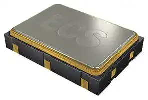
ETXO-L33CL-100.000
TCXO, 100 MHz, 2.5 ppm, SMD, 3.2mm x 2.5mm, LVDS, 3.3 V, ECSpressCON ETXO-L Series
⚠️ Reference pricing provided. In case of supply shortages, we will connect you with our trusted procurement partners to ensure your project's continuity.
- Manufacturer: ECS INC INTERNATIONAL
- Product type: Temperature Compensated - TCXO Oscillators
- SVHC: No SVHC (25-Jun-2025)
- Frequency Nom: 100MHz
- Product Range: ECSpressCON ETXO-L Series
- Supply Voltage Nom: 3.3V
- Frequency Stability + / -: 2.5ppm
- Operating Temperature Max: 85°C
- Operating Temperature Min: -30°C
- Oscillator Case / Package: SMD, 3.2mm x 2.5mm
- Oscillator Output Compatibility: LVDS
| Delivery and price | |
|---|---|
| Units per pack | 250 |
| Price | 8.27 € |
| Current stock | 10+ |
| Lead time | 30 days |
Datasheet

## **ECSpressCON[TM]**

ETXO-L2 (2.5V) and ETXO-L3 (3.3V) low jitter, low current SMD Temperature Compensated Crystal Oscillators (TCXO).

## **ETXO-L LVDS TCXO**

**Request a Sample** —J

## **OPERATING CONDITIONS / ELECTRICAL CHARACTERISTICS**

|**Parameters**|**Conditions**|**ETXO-L2 (+2.5V)**|**ETXO-L2 (+2.5V)**|**ETXO-L2 (+2.5V)**|**ETXO-L3 (+3.3V)**|**ETXO-L3 (+3.3V)**|**ETXO-L3 (+3.3V)**|**Units**|
|---|---|---|---|---|---|---|---|---|
|||**MIN**|**TYP**|**MAX**|**MIN**|**TYP**|**MAX**||
|**Frequency Range**<br>~~eS~~|~~eS~~|10.000<br>~~eS~~|~~eS~~|1500.00<br>~~eS~~|10.000<br>~~eS~~|~~eS~~|1500.00<br>~~eS~~|MHz<br>~~eS~~|
|**Operating Temperature**<br>~~eS~~|Standard (L Option)<br>~~eS~~|-30<br>~~eS~~|~~eS~~|+85<br>~~eS~~|-30<br>~~eS~~|~~eS~~|+85<br>~~eS~~|°C<br>~~eS~~|
||Extended (N Option)<br>~~eS~~|-40<br>~~eS~~|~~eS~~|+85<br>~~eS~~|-40<br>~~eS~~|~~eS~~|+85<br>~~eS~~|°C<br>~~eS~~|
|**Storage Temperature**<br>~~eS~~|~~eS~~|-55<br>~~eS~~|~~eS~~|+125<br>~~eS~~|-55<br>~~eS~~|~~eS~~|+125<br>~~eS~~|°C<br>~~eS~~|
|**Supply Voltage**<br>~~SS~~|VDD<br>~~SS~~|+2.375<br>~~SS~~|+2.5<br>~~SS~~|+2.625<br>~~SS~~|+3.135<br>~~SS~~|+3.3<br>~~SS~~|+3.465<br>~~SS~~|VDC<br>~~SS~~|
|**Frequency Stability ***<br>~~SS~~|Option A<br>~~SS~~|~~SS~~|~~SS~~|±2.5<br>~~SS~~|~~SS~~|~~SS~~|±2.5<br>~~SS~~|ppm<br>~~SS~~|
||Option B*<br>~~SS~~|~~SS~~|~~SS~~|±1.0<br>~~SS~~|~~SS~~|~~SS~~|±1.0<br>~~SS~~|ppm<br>~~SS~~|
|**Initial Calibration Tolerance**<br>~~SS~~|@+25°C ±2°C<br>~~SS~~|~~SS~~|~~SS~~|±1.0<br>~~SS~~|~~SS~~|~~SS~~|±1.0<br>~~SS~~|ppm<br>~~SS~~|
|**Current with output disabled**<br>~~SS~~|~~SS~~|~~SS~~|18<br>~~SS~~|~~SS~~|~~SS~~|18<br>~~SS~~|~~SS~~|mA<br>~~SS~~|
|**Input Current**|10.0~156.0 MHz|||22|||25|mA|
||156.1~600.0 MHz|||28|||30|mA|
||600.1~800.0 MHz|||30|||32|mA|
||800.1~1500.0 MHz|||34|||36|mA|
|**Duty Cycle**|@ 50% VCClevel|||45/55|||45/55|%|
|**Output Load**|Differential||||||||
|**Output Enable**|Pin 2**|0.7%|||0.7%|||Vdd|
|**Output Disable**|Pin 2**|||0.3%|||0.3%|Vdd|
|**Disable Current**|||18|||18||mA|
|**Output Enable Time**||||200|||200|ns|
|**Output Disable Time**|Pin 2=VIL|||50|||50|ns|
|**“0” Level**|VOL|0.9|1.1||0.9|1.1||V|
|**“1” Level**|VOH||1.4|1.6||1.4|1.6|V|
|**Rise and Fall Times**|10% VDD to 90% level|200||400|200||400|pS|
|**Aging**|@ +25°C (first year)|||±1|||±1|ppm|
|**Start-up Time**||||5|||5|ms|
|**Phase Jitter, rms**|12 KHz to 20 MHz band||1.0|||1.0||pS|
|**Absolute Voltage Range**||||+3.63|||+3.63|VDC|
|**Moisture Sensitivity Level**||1|||||||
|**Termination Finish**||Au|||||||
|**ESD Sensitivity**|Human BodyModel|3kV Max.|||||||


_*Note: Consult ECS for availability_

_**Note: Internal pull-up resistor active output if pin 2 is left open._

|**Part Number Guide: Example ETXO-L33CL-156.250**<br>**Series**<br>**Voltage**<br>**Package**<br>**Size (mm)**<br>**Stability**<br>**Operating**<br>**Temperature**<br>**-**<br>**Frequency**|**Part Number Guide: Example ETXO-L33CL-156.250**<br>**Series**<br>**Voltage**<br>**Package**<br>**Size (mm)**<br>**Stability**<br>**Operating**<br>**Temperature**<br>**-**<br>**Frequency**|**Part Number Guide: Example ETXO-L33CL-156.250**<br>**Series**<br>**Voltage**<br>**Package**<br>**Size (mm)**<br>**Stability**<br>**Operating**<br>**Temperature**<br>**-**<br>**Frequency**|**Part Number Guide: Example ETXO-L33CL-156.250**<br>**Series**<br>**Voltage**<br>**Package**<br>**Size (mm)**<br>**Stability**<br>**Operating**<br>**Temperature**<br>**-**<br>**Frequency**|**Part Number Guide: Example ETXO-L33CL-156.250**<br>**Series**<br>**Voltage**<br>**Package**<br>**Size (mm)**<br>**Stability**<br>**Operating**<br>**Temperature**<br>**-**<br>**Frequency**|**Part Number Guide: Example ETXO-L33CL-156.250**<br>**Series**<br>**Voltage**<br>**Package**<br>**Size (mm)**<br>**Stability**<br>**Operating**<br>**Temperature**<br>**-**<br>**Frequency**|**Part Number Guide: Example ETXO-L33CL-156.250**<br>**Series**<br>**Voltage**<br>**Package**<br>**Size (mm)**<br>**Stability**<br>**Operating**<br>**Temperature**<br>**-**<br>**Frequency**|
|---|---|---|---|---|---|---|
|ETXO-L<br>(LVDS<br>Output)|2 = +2.5V<br>3 = +3.3V|3 = 3.2 x 2.5|B = ± 1.0 ppm*<br>C = ± 2.5 ppm|L =   -30 ~ +85°C<br>M =  -20 ~ +70°C<br>N =   -40 ~ +85°C|-|Customer Specified|


**==> picture [70 x 39] intentionally omitted <==**

**----- Start of picture text -----**<br>
RO =|S<br>COMPLIANT<br>**----- End of picture text -----**<br>


## **ECSpressCON[TM] ETXO-L LVDS TCXO**

**Phase Noise and Jitter Data (typical)**

|**SSB**<br>**Phase**<br>**Noise**<br>**Data**<br>**(dBc/Hz**<br>**typical)**|**Frequency**<br>**(offset)**|**77.760**|**122.880**|**125.00**|**156.250**|**212.5**|
|---|---|---|---|---|---|---|
||10Hz|-64|-68|-63|-63|-62|
||100 Hz|-84|-99|-94|-91|-93|
||1 KHz|-118|-113|-113|-109|-105|
||10KHz|-128|-119|-118|-115|-113|
||100KHz|-137|-120|-119|-116|-115|
||1 MHz|-145|-140|-137|-138|-135|
||5MHz|-152|-142|-146|-147|-143|
|**Phase Jitter pS**<br>**12 KHz ~ 20 MHz,**<br>**RMS**||0.9|0.8|1.1|1.0|1.0|


**Phase Noise Plot of ETXO-L33CL-156.250 (typical)**

Single ~~pO~~ **Package Data Item Description** Lid Metal Base Ceramic Source Plating Gold/Nickel Surface/Under

## RoHS

**ECSpressCON[TM] ETXO-L LVDS TCXO**

## **Dimensions (mm)**

**==> picture [89 x 80] intentionally omitted <==**

**----- Start of picture text -----**<br>
3.2401<br>ste")<br>2.0402<br>**----- End of picture text -----**<br>


**==> picture [109 x 57] intentionally omitted <==**

**----- Start of picture text -----**<br>
==<br>tee:<br>~ Seo<br>1.28+>+-1.28<br>**----- End of picture text -----**<br>


**Pin Connections** Pin # Function ~~a a~~ 1 No Connect ~~ee~~ 2 Output Enable ~~a~~ 3 Ground 4 Differential Output 5 Complementary Output 6 Supply Voltage ~~ee a~~

_Figure 1) Top, Side, Bottom & Land_
Updated at April 16, 2026
About Novapart
Novapart is a B2B electronic component broker specialising in stock shortages and cost reduction. We source hard-to-find parts and identify compliant alternatives across a catalogue of 420,000+ components from 500+ manufacturers.
Learn more →Stock Shortage Specialist
When a component is unavailable, discontinued or has an unacceptable lead time, we tap into our network of vetted European and Asian distributors to source what you need — without compromising on quality or traceability.
Request a quote →Compliant Alternatives
We identify pin-to-pin, electrically equivalent substitutes that meet the same certifications (RoHS, AEC-Q100, REACH) as your original specification — validated against datasheets, not just part numbers. Often at a lower cost.
BOM Analysis service →