
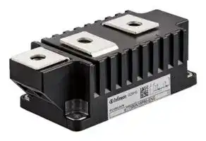


ETT630N18P60HPSA1
Thyristor Diode Module, 1.8 kV, 700 A, 2 V Vgt, 0.25 A Igt, 20 kA Itsm
- Manufacturer: INFINEON
- Product type: Thyristors - SCR Modules
- SVHC: No SVHC (25-Jun-2025)
- No. of Pins: 7Pins
- Product Range: -
- SCR Module Type: Series Connected - SCRs
- Thyristor Mounting: Panel
- On State RMS Current: 700A
- Thyristor Case Style: Module
- Average Forward Current: 628A
- Gate Trigger Current Max: 250mA
- Gate Trigger Voltage Max: 2V
- Operating Temperature Max: 135°C
- Repetitive Peak Reverse Voltage: 1.8kV
- Peak Repetitive Off State Voltage: 1.8kV
| Delivery and price | |
|---|---|
| Units per pack | 5 |
| Price | 230.39 € |
| Current stock | 10+ |
| Lead time | 30 days |
**Technische Information / technical information**
## **Netz-Thyristor-Modul Phase Control Thyristor Module**
## **eTT630N18P60**
## **Key Parameters**
VDRM / VRRM 1800V ITAVM 628A (TC=85°C) ITSM 20000A VT0 0,8V rT 0,341mΩ RthJC 0,0575K/W Base plate 60mm
For type designation please refer to actual short form catalog
http://www.ifbip.com/catalog
## **Merkmale**
- Druckkontakt-Technologie für hohe Zuverlässigkeit
- Advanced Medium Power Technology (AMPT)
- Industrie-Standard-Gehäuse
- Elektrisch isolierte Bodenplatte
## **Features**
- Pressure contact technology for high reliability
- Advanced Medium Power Technology (AMPT)
- Industrial standard package
- Electrically insulated base plate
## **Typische Anwendungen**
- Sanftanlasser
- Gleichrichter für Antriebsapplikationen
- Kurzschließer-Applikationen
- Leistungssteller
- Gleichrichter für UPS
- Batterieladegleichrichter
- Statische Umschalter
- Bypass-Schalter
## **Typical Applications**
- Soft starter
- Rectifier for drives applications
- Crowbar applications
- Power controllers
- Rectifiers for UPS
- Battery chargers
- Static switches
- Bypass switches
~~Se|~~ content of customer DMX code DMX code DMX code digit digit quantity ~~a~~ serial number 1..5 5 ~~a~~ SAP material number 6..12 7 ~~a~~ Internal production order number 13..20 8 ~~a~~ datecode (production year) 21..22 2 ~~a~~ datecode (production week) 23..24 2
**==> picture [132 x 55] intentionally omitted <==**
**----- Start of picture text -----**<br>
TT TD<br>www.ifbip.com<br>-<br>a support@infineon bip.com<br>**----- End of picture text -----**<br>
Date of Publication 2021-02-24
1/11
Seite/page
Revision: 3.1
## **Technische Information / technical information**
## **Netz-Thyristor-Modul**
## **Phase Control Thyristor Module**
## **eTT630N18P60**
**eTT630N18P60**
**eTD630N18P60**
||**Technische Information /**<br>**technical information**|**Technische Information /**<br>**technical information**|**Technische Information /**<br>**technical information**|o-..<br>Cinfineon|o-..<br>Cinfineon|
|---|---|---|---|---|---|
|**Netz-Thyristor-Modul**<br>**Phase Control Thyristor Module**|**eTT630N18P60**|||Infineon Technologies Bipolar<br>GmbH & Co. KG||
|**Elektrische Eigenschaften / Electrical properties**<br>HöchstzulässigeWerte /Maximum ratedvalues<br>**eTT630N18P60**<br>**eTD630N18P60**<br>Periodische Vorwärts- und Rückwärts-Spitzensperrspannung<br>repetitive peak forward off-state and reverse voltages<br>Tvj= -40°C... Tvj max<br>VDRM,VRRM <br>1800 V<br>Vorwärts-Stoßspitzensperrspannung<br>non-repetitive peak forward off-state voltage<br>Tvj= -40°C... Tvj max<br>VDSM<br>1800<br>V<br>Rückwärts-Stoßspitzensperrspannung<br>non-repetitive peak reverse voltage<br>Tvj= +25°C... Tvj max<br>VRSM<br>1900<br>V<br>Durchlaßstrom-Grenzeffektivwert<br>maximum RMS on-state current<br>ITRMSM<br>700 A<br>Dauergrenzstrom<br>average on-state current<br>TC= 85°C<br>ITAVM<br>628<br>A<br>Stoßstrom-Grenzwert<br>surge current<br>Tvj= 25°C, tP= 10ms<br>Tvj= Tvj max, tP= 10ms<br>ITSM<br>20000<br>16800<br>A<br>A<br>Grenzlastintegral<br>I²t-value<br>Tvj= 25°C, tP= 10ms<br>Tvj= Tvj max, tP= 10ms<br>I²t<br>2000000<br>1411200<br>A²s<br>A²s<br>Kritische Stromsteilheit<br>critical rate of rise of on-state current<br>DIN IEC 747-6<br>f = 50Hz, iGM= 1A, diG/dt = 1A/µs<br>(diT/dt)cr<br>200 A/µs<br>Kritische Spannungssteilheit<br>critical rate of rise of off-state voltage<br>Tvj= Tvj max, vD= 0,67 VDRM<br>(dvD/dt)cr<br>1000 V/µs<br>CharakteristischeWerte / Characteristicvalues<br>Durchlaßspannung<br>on-state voltage<br>Tvj= Tvj max, iT= 1500 A<br>vT<br>max.<br>1,45<br>V<br>Schleusenspannung<br>threshold voltage<br>Tvj= Tvj max<br>V(TO)<br>max.<br>0,8 V<br>Ersatzwiderstand<br>slope resistance<br>Tvj= Tvj max<br>rT<br>max. 0,341 mΩ<br>Zündstrom<br>gate trigger current<br>Tvj= 25°C, vD= 12V<br>IGT<br>max.<br>250 mA<br>Zündspannung<br>gate trigger voltage<br>Tvj= 25°C, vD= 12V<br>VGT<br>max.<br>2 V<br>Nicht zündender Steuerstrom<br>gate non-trigger current<br>Tvj= Tvj max, vD= 12V<br>Tvj= Tvj max, vD= 0,5 VDRM<br>IGD<br>max.<br>max.<br>10<br>5<br>mA<br>mA<br>Nicht zündende Steuerspannung<br>gate non-trigger voltage<br>Tvj= Tvj max, vD= 0,5 VDRM<br>VGD<br>max.<br>0,25 V<br>Haltestrom<br>holding current<br>Tvj= 25°C, vD= 12V, RA= 1Ω<br>IH<br>max.<br>300 mA<br>Einraststrom<br>latching current<br>Tvj= 25°C, vD= 12V, RGK≥ 10Ω<br>iGM= 1A, diG/dt = 1A/µs, tg= 20µs<br>IL<br>max.<br>1500 mA<br>Vorwärts- und Rückwärts-Sperrstrom<br>forward off-state and reverse current<br>Tvj= Tvj max<br>vD= VDRM, vR= VRRM<br>iD, iR<br>max.<br>110 mA<br>Zündverzug<br>gate controlled delay time<br>DIN IEC 747-6<br>Tvj= 25°C, iGM= 1A, diG/dt = 1A/µs<br>tgd<br>max.<br>4 µs<br>prepared by: AG<br>date of publication: 2021-02-24<br>approved by: ML<br>revision:<br>3.1||||||
|Date of Publication 2021-02-24||Revision: 3.1|Seite/page||2/11|
2/11
Seite/page
Date of Publication 2021-02-24
Revision: 3.1
## **Technische Information / technical information**
## **Netz-Thyristor-Modul Phase Control Thyristor Module**
## **eTT630N18P60**
||**Technische Information /**<br>**technical information**|**Technische Information /**<br>**technical information**|**Technische Information /**<br>**technical information**|o-..<br>Cinfineon|o-..<br>Cinfineon|
|---|---|---|---|---|---|
|**Netz-Thyristor-Modul**<br>**Phase Control Thyristor Module**|**eTT630N18P60**|||Infineon Technologies Bipolar<br>GmbH & Co. KG||
|ThermischeEigenschaften<br>Mechanische Eigenschaften<br>**Elektrische Eigenschaften / Electrical properties**<br>Charakteristische Werte / Characteristic values<br>Freiwerdezeit<br>circuit commutated turn-off time<br>Tvj= Tvj max, iTM= ITAVM<br>vRM= 100 V, vDM= 0,67 VDRM<br>dvD/dt = 20 V/µs, -diT/dt = 10 A/µs<br>tq<br>typ.<br>270<br>µs<br>Isolations-Prüfspannung<br>insulation test voltage<br>RMS, f = 50 Hz, t = 1min<br>RMS, f = 50 Hz, t = 1sec<br>VISOL<br>3,0<br>3,6<br>kV<br>kV<br>**Thermische Eigenschaften / Thermal properties**<br>Innerer Wärmewiderstand<br>thermal resistance, junction to case<br>pro Modul / per Module, Θ = 180° sin<br>pro Zweig / per arm, Θ = 180° sin<br>pro Modul / per Module, DC<br>pro Zweig / per arm, DC<br>RthJC<br>max.<br>max.<br>max.<br>max.<br>0,030<br>0,060<br>0,0288<br>0,0575<br>K/W<br>K/W<br>K/W<br>K/W<br>Übergangs-Wärmewiderstand<br>thermal resistance, case to heatsink<br>pro Modul / per Module<br>pro Zweig / per arm<br>RthCH<br>typ.<br>typ.<br>0,015<br>0,030<br>K/W<br>K/W<br>Höchstzulässige Sperrschichttemperatur<br>maximum junction temperature<br>Tvj max<br>135 °C<br>Betriebstemperatur<br>operating temperature<br>Tc op<br>-40...+135 °C<br>Lagertemperatur<br>storage temperature<br>Tstg<br>-40...+135 °C<br>**Mechanische Eigenschaften / Mechanicalproperties**<br>Gehäuse, siehe Anlage<br>case, see annex<br>Seite 4<br>page 4<br>Si-Element mit Druckkontakt<br>Si-pellet with pressure contact<br>Innere Isolation<br>internal insulation<br>Basisisolierung (Schutzklasse 1, EN61140)<br>Basic insulation (class 1, IEC61140)<br>AlN<br>Anzugsdrehmoment für mechanische Anschlüsse<br>mounting torque<br>Toleranz / Tolerance ± 15%<br>M1<br>6<br>Nm<br>Anzugsdrehmoment für elektrische Anschlüsse<br>terminal connection torque<br>Toleranz / Tolerance ± 10%<br>M2<br>12<br>Nm<br>Steueranschlüsse<br>control terminals<br>DIN 46 244<br>A 2,8 x 0,8<br>Gewicht<br>weight<br>G<br>typ.<br>830 g<br>Kriechstrecke<br>creepage distance<br>19 mm<br>Schwingfestigkeit<br>vibration resistance<br>f = 50 Hz<br>50 m/s²<br>file-No.<br>E 83335<br>.<br>A||||||
|Date of Publication 2021-02-24||Revision: 3.1|Seite/page||3/11|
3/11
Seite/page
Date of Publication 2021-02-24
Revision: 3.1
**Technische Information / technical information**
d **Netz-Thyristor-Modul Phase Control Thyristor Module**
## **eTT630N18P60**
**==> picture [461 x 449] intentionally omitted <==**
**----- Start of picture text -----**<br>
screwing depth max.18 plug A 2.8x0.8<br>Ly ar a r ty | 4 | H E gl |<br>|_|J H HH EH YHLr / IL| p f le! li} L<br>6.5±0.2<br>(44) 50±0.5 44±0.5<br>M10<br>13±0.5<br>30±1<br>S ET atk te icy)<br>25±0.3 25±0.3<br>112±0.3<br>124±0.5 base plate<br>127.5±1.5<br>145.6 [+2]<br>-1<br>1 2 3 1 2 3<br>4 5 7 6 4 5<br>TT TD<br>52±1<br>10±0.2<br>late<br>p<br>36±1<br>48±0.3 36±1 28±0.3 64±1.5<br>60±0.5 base<br>**----- End of picture text -----**<br>
4/11
Seite/page
Date of Publication 2021-02-24
Revision: 3.1
**Technische Information / technical information**
## **Netz-Thyristor-Modul Phase Control Thyristor Module** a
## **eTT630N18P60**
**Analytische Elemente des transienten Wärmewiderstandes ZthJC für DC Analytical elements of transient thermal impedance ZthJC for DC**
|**Netz-Thyristor-Modul**<br>**Phase Control Thyristor Module**<br>**eTT630N18P60**<br>a<br>“ermH Co K“_<br>GmbH & Co. KG|**Netz-Thyristor-Modul**<br>**Phase Control Thyristor Module**<br>**eTT630N18P60**<br>a<br>“ermH Co K“_<br>GmbH & Co. KG|**Netz-Thyristor-Modul**<br>**Phase Control Thyristor Module**<br>**eTT630N18P60**<br>a<br>“ermH Co K“_<br>GmbH & Co. KG|**Netz-Thyristor-Modul**<br>**Phase Control Thyristor Module**<br>**eTT630N18P60**<br>a<br>“ermH Co K“_<br>GmbH & Co. KG|**Netz-Thyristor-Modul**<br>**Phase Control Thyristor Module**<br>**eTT630N18P60**<br>a<br>“ermH Co K“_<br>GmbH & Co. KG|**Netz-Thyristor-Modul**<br>**Phase Control Thyristor Module**<br>**eTT630N18P60**<br>a<br>“ermH Co K“_<br>GmbH & Co. KG|**Netz-Thyristor-Modul**<br>**Phase Control Thyristor Module**<br>**eTT630N18P60**<br>a<br>“ermH Co K“_<br>GmbH & Co. KG|**Netz-Thyristor-Modul**<br>**Phase Control Thyristor Module**<br>**eTT630N18P60**<br>a<br>“ermH Co K“_<br>GmbH & Co. KG|
|---|---|---|---|---|---|---|---|
|**Analytische Elemente des transienten Wärmewiderstandes ZthJC für DCthJC für DC für DC**<br>**Analytical elements of transient thermal impedance ZthJC for DCthJC for DC for DC**||||||||
|Pos. n|1|2|3|4|5|6|7|
|Rthn[K/W]|0,011|0,0159|0,02255|0,00811||||
|τn[s]|5,6|2,56939|0,8|0,00165||||
|Analytische Funktion / Analytical function:<br><br><br><br>max<br>n<br>n=1<br>thn<br>thJC<br>n<br>– t<br>- e<br>1<br>R<br>Z||||||||
**Erhöhung des Zth DC bei Sinus und Rechteckströmen mit unterschiedlichen Stromflusswinkeln Θ Rise of Zth DC for sinewave and rectangular current with different current conduction angles Θ ΔZth Θ rec / ΔZth Θ sin**
||Θ = 180°|Θ = 120°|Θ = 90°|Θ = 60°|Θ = 30°|
|---|---|---|---|---|---|
|ΔZth Θ rec<br>[K/W]|0,00825|0,01604|0,02304|0,03443|0,05412|
|ΔZth Θ sin<br>[K/W]|0,00251|0,00570|0,01102|0,02157|0,04358|
Zth Θ rec = Zth DC + Zth Θ rec
Zth Θ sin = Zth DC + Zth Θ sin
5/11
Seite/page
Date of Publication 2021-02-24
Revision: 3.1
## **Technische Information / technical information**
## **Diagramme Netz-Thyristor-Modul Phase Control Thyristor Module**
## **eTT630N18P60**
**==> picture [491 x 232] intentionally omitted <==**
**----- Start of picture text -----**<br>
0,070 SBGO<br>poeee eee<br>0,060 ROBBBspoBO OOOssO OOOO Osee [OO] OO [OO] OOOO OOG [e] G OO<br>PoePoeSeeeeeTT<br>0,050 PoeaBOsOeeeSee [eee] OO2eedOkeee [eee] eeQO<br>BBss GO Oe ee<br>BOEe es OO OoOO<br>0,040 poaaeea eeee eeeeee eeee02 eeeeee ee eeeeeeeeeeeee eeeeee<br>po e eeeee<br>0,030 esesessO BO OO OOA sOOO<br>po OO OG OO<br>BBBBssBOOOGO2 02424 OOOOOOOOOOOO OS OGOG OO<br>0,020<br>po BO es<br>OO OO ee<br>0,010 poOeaaOOBsa SS SSaaes ee ereee aOOae ee Sseee PeeesHOa esOOOOeOeeeOe eeOOsOOO e GDOQO e ee ONGOe OOOO ee 0eeGGeI eeSG<br>0,000<br>0,01 0,1 t [s] 1 10 100<br>[K/W]<br>(th)JC<br>Z<br>**----- End of picture text -----**<br>
**Transienter innerer Wärmewiderstand je Zweig / Transient thermal impedance per arm ZthJC = f(t)**
**==> picture [497 x 329] intentionally omitted <==**
**----- Start of picture text -----**<br>
Durchgangsverluste<br>Parameter: Stromflußwinkel Θ / Current conduction angle Θ<br>100 —ee(SSee<br>po<br>po<br>10 c<br>a STS<br>aes b SS<br>po eer a S= Se<br>ee eers ee ee ee ee Nee TT<br>po ee = ae<br>a enee ee<br>1<br>a————— 2 Aeeee ee<br>——zr_eee—aueeeeee eeeeee e AlFea| ace acea(GGOees ee ee<br>BE Albee<br>0,1<br>10 100 iG [mA] 1000 10000<br>Steuercharakteristik vG = f (iG) mit Zündbereichen für VD = 12 V<br>Gate characteristic vG = f (iG) with triggering area for VD = 12 V<br> [V]<br>G<br>v = -40 CTvj<br> = = +25 CTvj<br>vj max<br>T +135 C<br>**----- End of picture text -----**<br>
Höchstzulässige Spitzensteuerverlustleistung / Maximum rated peak gate power dissipation PGM = f (tg) :
a - 20W/10ms b - 40W/1ms c - 60W/0,5ms
6/11
Seite/page
Date of Publication 2021-02-24
Revision: 3.1
## **Technische Information /**
## **technical information**
## **Netz-Thyristor-Modul Phase Control Thyristor Module**
## **eTT630N18P60**
**==> picture [497 x 571] intentionally omitted <==**
**----- Start of picture text -----**<br>
800<br>DC<br>700 REE PtE tT {Tt t_ tt ttt cE TdT TC TcrE rE TT rE rE TT ET ceEE<br>ee<br>600 Pi tt tt] tT tt dt dT Ttee{Tt eee 180 rec ||PrittAe<br>180 sin<br>Pt 120 rec [| i<br>500 Pt tt eet tt tt tt 90 rec L Lat | | | ft tt<br>Pt | {ttt| te tT ttyttt ff 60 rec Aa |Zaprl 2g| | ttteeetteeett<br>400 Q = 30 rec<br>H e ZW Zac an eee eee<br>Pt | | ty Ve7Z2e 4 eee eee<br>300 SRR RRR Ae ZZ eeeeee<br>SRR eee<br>SRR 22 Z Aeeee<br>200<br>See 272 Zee eee eee eee<br>| DW Gehäusetemperatur bei Rechteck 2 ee eee eee<br>100 | | | aA et TT ET TTT<br>Bna2<br>0 rast tT | dT fT TT ET] TT | | fT fT EET TT ET fT fT<br>0 100 200 300 400 500 600 700 800<br>ITAV [A]<br>Durchlassverlustleistung je Zweig / On-state power loss per arm PTAV = f(ITAV)<br>Strombelastung je Zweig / Current load per arm<br>Berechnungsgrundlage PTAV (Schaltverluste gesondert berücksichtigen)<br>Calculation base PTAV (switching losses should be considered separately)<br>Parameter: Stromflußwinkel / Current conduction angle Θ<br>140<br>ee ee eee<br>120<br>Sa SS == Se ee Re eee<br>Pt | PN eeRSSseesereet Ett Pty Ty ey tt<br>100<br>SERERERNERNa Ss te See eee<br>Se ee<br>Oe ee eee<br>80<br>ee Ee ee<br>Oe eeeee<br>60<br>180 sin<br>40 S RRS Eeeee LEEeeEE EL EL<br>20 || | | {| y Q = 30 rec 60 rec 90 rec 120 rec 180 rec Fit| tty DC | |fy<br>0 100 200 300 400 500 600 700 800<br>ITAVM [A]<br>[W]<br>TAV<br>P<br>[°C]<br>C<br>T<br>**----- End of picture text -----**<br>
## **Höchstzulässige Gehäusetemperatur / Maximum allowable case temperature TC = f(ITAVM)**
Strombelastung je Zweig / Current load per arm
**Berechnungsgrundlage PTAV (Schaltverluste gesondert berücksichtigen) Calculation base PTAV (switching losses should be considered separately)**
Parameter: Stromflußwinkel Θ / Current conduction angle Θ
7/11
Seite/page
Date of Publication 2021-02-24
Revision: 3.1
**==> picture [146 x 23] intentionally omitted <==**
**----- Start of picture text -----**<br>
Technische Information /<br>technical information<br>**----- End of picture text -----**<br>
## **Netz-Thyristor-Modul Phase Control Thyristor Module eTT630N18P60**
**==> picture [508 x 217] intentionally omitted <==**
**----- Start of picture text -----**<br>
2800<br>2600 0,10 aa ee RthCA [K/W] - B2 => ID pi SRR | | | f | Pe | pe<br>+<br>2400 po aNT pt ty || PP| tT Pe tp PPpT<br>2200 EE 0,12 IN-TN| TT ~ PittSREYtT | tT Pe te PP PhP TT<br>pt UN N pit ty tp pe Pt | |<br>2000 0,15 R-Last<br>RY ptt | Pt | | AA | |<br>R-load<br>1800 P|ENN NENT - pit | Pe PP Ye| | |<br>1600 0,20<br>R R ptt | | tT Pe tT PP Pt tt TT yy<br>NA NNR ENN IIRO T Pipt t t Ty yyte eePP Pr PP Tt Ve L-Last ||<br>1400 0,25 | Sh NTN IR Pi i | tt PP Pr Pe L-load =<br>1200 0,30 SPSS NSONSET]' FERREZr<br>1000<br>0,40 PSSST— [SS PEE 7PA<br>800<br>S SS] EEE<br>0,60<br>600<br>0,80 PSSST][———. —_] a N FEES& |<br>400 1,00<br>200 2,00<br>0<br>20 40 60 80 100 120 0 200 400 600 800 1000<br>1,00 2,00 T A [°C] I D [A]<br> [W]<br> tot<br>P<br>Achsentitel<br>**----- End of picture text -----**<br>
## **Höchstzulässiger Ausgangsstrom / Maximum rated output current ID**
B2- Zweipuls-Brückenschaltung / Two-pulse bridge circuit
Gesamtverlustleistung der Schaltung / Total power dissipation at circuit Ptot
Parameter:
Wärmewiderstand pro Element zwischen den Gehäusen und Umgebung / Thermal resistance per chip cases to ambient RthCA
**==> picture [507 x 218] intentionally omitted <==**
**----- Start of picture text -----**<br>
3500 po S 0,10 [ NfSTT R thCA [K/W] B6 — ID + pot=FRERREESSEeeeof ft pp ep EEE EEE<br>0,12 {oN e eee<br>SeeNE DN ee 3~ pot fy fp fp yp a eee<br>3000 pT NN eee<br>[NNT eee<br>S 0,15 S - eee<br>2500 popoa N 0,20 INfo[ONTENIENTENE [N] NNNNNENTeSN eee [NR] NN ee [ee] =e eeT potpotpot e eeeeefyfyfy fpftfp ppPppppp epedeeaa e eeaeee eeeeeeeaeee.eeee eee eeeeeeeeeeee<br>2000 PSPS 0,25 NOON| WSNOS OSSNIINNNNIK potpopeefttf tppppppp ppaeaAee eee<br>1500 PORN 0,30 ORR] EERE<br>0,40 PSS ORS FERRE<br>> a N N N a<br>0,50<br>1000<br>0,60 S SSNeeoe eeeee<br>SSR eee eeeeee<br>0,80 eS FEE<br>500 1,00 es— eeT—-ee eeeEES OSSSSSRSAACee, DON ASS poyaeeyy rae ee<br>1,502,00 eS , SESESSIR OSEee ee ee ee eee<br>0 a ce ee eee<br>20 40 60 80 100 120 0 100 200 300 400 500 600 700 800 900 1000 1100 1200 1300<br>T A [°C] ID [A]<br> [W]<br> tot<br>P<br>**----- End of picture text -----**<br>
## **Höchstzulässiger Ausgangsstrom / Maximum rated output current ID**
B6- Sechspuls-Brückenschaltung / Six-pulse bridge circuit Gesamtverlustleistung der Schaltung / Total power dissipation at circuit Ptot Parameter: Wärmewiderstand pro Element zwischen den Gehäusen und Umgebung / Thermal resistance per chip cases to ambient RthCA
8/11
Seite/page
Date of Publication 2021-02-24
Revision: 3.1
**==> picture [146 x 23] intentionally omitted <==**
**----- Start of picture text -----**<br>
Technische Information /<br>technical information<br>**----- End of picture text -----**<br>
## **Netz-Thyristor-Modul Phase Control Thyristor Module eTT630N18P60**
**==> picture [506 x 652] intentionally omitted <==**
**----- Start of picture text -----**<br>
1600<br>1500 0,08 R thCA K/W] W~1C<br>1400 p Aj o | _ ' IRMS PTPitttT tT tTtT TTTT tTiT tte tt EE EEEE ETET ff<br>13001200 0,10 PKNEN| [fdtT | | PittPi tittT tttTTT tttt_t_ tt tT ttEEE Tt]ET tf|<br>0,12<br>1100 ~<br>NININGE TT Pitt tT TT tt tTrT EE EE EE<br>1000 0,15<br>900 ————EmNmENN Nf] PittPEt TTPtT Tt tTTT tttTP eT EEAEE<br>800 0,20 POI NNN et LELELELE ELE ELL LLL LL EL<br>700 0,25 Wn NUNN PT TTT TT TT TT ee ee<br>600 0,30 MOKA NNT Pitt; Tit TTT TT ree<br>500 MASA NANA EEEEe<br>0,40<br>400 0,50 TEA SS AT Pitt TT tT Trlr EE EE EE<br>300 0,60 SS SN Pitt tt} ee TE EE Tt<br>0,80<br>200 1,00 — SSS Pit tere<br>100 2,00 SSE oO Bp ae<br>0 >a<br>20 40 60 80 100 120 0 100 200 300 400 500 600 700 800 900 1000 1100<br>TA [°C] I RMS [A]<br>Höchstzulässiger Effektivstrom / Maximum rated RMS current IRMS<br>W1C - Einphasen-Wechselwegschaltung / Single-phase inverse parallel circuit<br>Gesamtverlustleistung der Schaltung / Total power dissipation at circuit Ptot<br>Parameter:<br>Wärmewiderstand pro Element zwischen den Gehäusen und Umgebung /<br>Thermal resistance per chip cases to ambient RthCA<br>5000<br>W3C<br>ee R thCA [K/W] ; ~ ~ ~ TL LLLLELLELLLIELLLLLLILLLL<br>4500 0,08 IRMS<br>esNTL : PEELEFCOEEEEELELELELLELELE I<br>4000 0,10<br>P EN ~ ~ ~ LL LLL<br>NIN FOE EEEEEEEEEEEEEE LEE]<br>3500 0,12 PCE EEE EEE ELLE LL]<br>Pp NNN) [SON] e s ee<br>3000 0,15<br>pONOSRNIR OePCEESEEEE ELLE ELLE<br>2500<br>0,20<br>P NAS PEPER PEPE PEPE yer<br>SS<br>2000 0,25 PKESSA] Eee<br>0,30 SNCS) See eee<br>1500 NES OR ENSAN] EEE eae<br>0,40 TT SN SAASRT<br>0,50<br>1000 0,60 We TOPCE<br>0,80 SSS ESSS-SSS S S SSSASA] EEEOPCEEE<br>500 1,00 SSSR:<br>2,00 OOSSSESRRRqEqQEBEQQRSSAA TOEeOST LEe e e<br>0 ES SESS SCeee<br>20 40 60 80 100 120 0 100 200 300 400 500 600 700 800 900 1000 1100<br>T A [°C] I RMS [A]<br>Höchstzulässiger Effektivstrom / Maximum rated RMS current IRMS<br>W3C - Dreiphasen-Wechselwegschaltung / Three-phase inverse parallel circuit<br>Gesamtverlustleistung der Schaltung / Total power dissipation at circuit Ptot<br>Parameter:<br>Wärmewiderstand pro Element zwischen den Gehäusen und Umgebung /<br>Thermal resistance per chip cases to ambient RthCA<br>[W]<br> tot<br>P<br> [W]<br> tot<br>P<br>**----- End of picture text -----**<br>
9/11
Seite/page
Date of Publication 2021-02-24
Revision: 3.1
## **Technische Information / technical information**
**Netz-Thyristor-Modul Phase Control Thyristor Module eTT630N18P60**
**==> picture [482 x 308] intentionally omitted <==**
**----- Start of picture text -----**<br>
10000<br>esa GGes a eeSS GS(GSOcc OO<br>popo iTM =<br>po er<br>pf EYa<br>re ee anee ee<br>|peeee<br>1000<br>ce =e} Pt tt<br>ne ee (<br>a aen Bae Baa Beee Beee ieBe Beee Rses<br>ne ee ee ree ie Bie lie Mes ne ee es es ed<br>a a i a ee a es ee es Qe GD<br>es es OO Qe Qe<br>100<br>1 10 -di/dt [A/µs] 100<br>Sperrverzögerungsladung / Recovered charge Qr = f(-di/dt)<br>Tvj = Tvjmax, vR ≤ 0,5 VRRM, vRM = 0,8 VRRM<br>Parameter: Durchlaßstrom / On-state current iTM<br>Q [µAs]r<br>**----- End of picture text -----**<br>
**==> picture [19 x 75] intentionally omitted <==**
**----- Start of picture text -----**<br>
iTM =<br>1000A<br>500A<br>200A<br>100A<br>50A<br>**----- End of picture text -----**<br>
**==> picture [489 x 323] intentionally omitted <==**
**----- Start of picture text -----**<br>
11.000<br>po<br>po<br>10.000<br>a<br>9.000 poa a ee ee ee pF —}a—_}_+_}ee ee eee++}<br>ars ee a ee ee ee A GD<br>8.000 ee 7 TA = 35 C | fT [ft]<br>Ds | | | |<br>7.000 es | |<br>a GO OG Ns RG<br>poST<br>6.000<br>apoa ee CODs SOOO<br>5.000<br>poZENE<br>PoEE<br>4.000<br>po<br>3.000 aeee a ee es es Oe es a es ee<br>Poepee<br>2.000 pooptd<br>po Ne tr<br>1.000 poaN<br>e b n TA = 45 C<br>0 ees es Oe Oe a aan<br>0,01 0,1 1<br>t [s]<br>Grenzstrom / Maximum overload on-state current IT(OV)M = f(t), vRM = 0,8 VRRM<br>a: Leerlauf / No-load conditions<br>b: nach Belastung mit ITAVM / after load with ITAVM<br>TA = 35°C, verstärkte Luftkühlung / Forced air cooling<br>TA = 45°C, Luftselbstkühlung / Natural air cooling<br>[A]<br>IT(OV)M<br>**----- End of picture text -----**<br>
10/11
Seite/page
Date of Publication 2021-02-24
Revision: 3.1
**Technische Information / technical information**
**Netz-Thyristor-Modul Phase Control Thyristor Module**
## **eTT630N18P60**
## Nutzungsbedingungen
Die in diesem Produktdatenblatt enthaltenen Daten sind ausschließlich für technisch geschultes Fachpersonal bestimmt. Die Beurteilung der Eignung dieses Produktes für Ihre Anwendung sowie die Beurteilung der Vollständigkeit der bereitgestellten Produktdaten für diese Anwendung obliegt Ihnen bzw. Ihren technischen Abteilungen.
In diesem Produktdatenblatt werden diejenigen Merkmale beschrieben, für die wir eine liefervertragliche Gewährleistung übernehmen. Eine solche Gewährleistung richtet sich ausschließlich nach Maßgabe der im jeweiligen Liefervertrag enthaltenen Bestimmungen. Garantien jeglicher Art werden für das Produkt und dessen Eigenschaften keinesfalls übernommen.
Sollten Sie von uns Produktinformationen benötigen, die über den Inhalt dieses Produktdatenblatts hinausgehen und insbesondere eine spezifische Verwendung und den Einsatz dieses Produktes betreffen, setzen Sie sich bitte mit dem für Sie zuständigen Vertriebsbüro in Verbindung. Für Interessenten halten wir Application Notes bereit.
Aufgrund der technischen Anforderungen könnte unser Produkt gesundheitsgefährdende Substanzen enthalten. Bei Rückfragen zu den in diesem Produkt jeweils enthaltenen Substanzen setzen Sie sich bitte ebenfalls mit dem für Sie zuständigen Vertriebsbüro in Verbindung.
Sollten Sie beabsichtigen, das Produkt in gesundheits- oder lebensgefährdenden oder lebenserhaltenden Anwendungsbereichen einzusetzen, bitten wir um Mitteilung. Wir weisen darauf hin, dass wir für diese Fälle
- die gemeinsame Durchführung eines Risiko- und Qualitätsassessments;
- den Abschluss von speziellen Qualitätssicherungsvereinbarungen;
- die gemeinsame Einführung von Maßnahmen einer laufenden Produktbeobachtung dringend empfehlen und gegebenenfalls die Belieferung von der Umsetzung solcher Maßnahmen abhängig machen.
Soweit erforderlich, bitten wir Sie, entsprechende Hinweise an Ihre Kunden zu geben.
Inhaltliche Änderungen dieses Produktdatenblatts bleiben vorbehalten.
## Terms & Conditions of usage
The product data contained in this product data sheet is exclusively intended for technically trained staff. You and your technical departments will have to evaluate the suitability of the product for the intended application and the completeness of the product data with respect to such application.
This product data sheet is describing the specifications of this product for which a warranty is granted. Any such warranty is granted exclusively pursuant the terms and conditions of the supply agreement. There will be no guarantee of any kind for the product and its specifications.
Should you require product information in excess of the data given in this product data sheet or which concerns the specific application of our product, please contact the sales office, which is responsible for you. For those that are specifically interested we may provide application notes.
Due to technical requirements our product may contain dangerous substances. For information on the types in question please contact the sales office, which is responsible for you.
Should you intend to use the Product in health or live endangering or life support applications, please notify. Please note, that for any such applications we urgently recommend
- to perform joint Risk and Quality Assessments;
- the conclusion of Quality Agreements;
- to establish joint measures of an ongoing product survey, and that we may make delivery depended on the realization of any such measures.
If and to the extent necessary, please forward equivalent notices to your customers.
Changes of this product data sheet are reserved.
11/11
Seite/page
Date of Publication 2021-02-24
Revision: 3.1
Updated at June 7, 2026
Infineon Technologies is a globally recognized leader in semiconductor solutions, renowned for driving innovation in power management, energy efficiency, and modern mobility. With a strong legacy of engineering excellence, the company provides highly reliable components designed to meet the rigorous demands of industrial, automotive, and advanced commercial applications. The core of our Infineon portfolio is centered on their industry-leading discrete semiconductors. We offer an extensive selection of single and dual MOSFETs, alongside a robust range of single IGBTs and advanced IGBT modules. These flagship power transistors are essential for high-efficiency power conversion and motor control, providing engineers with superior thermal performance and minimized switching losses. Beyond advanced field-effect transistors, the selection includes a comprehensive array of diodes and rectifiers, heavily featuring Schottky diodes, as well as fast-recovery and RF/PIN diodes. This power foundation is further supported by bipolar transistors, intelligent power modules, and thyristor SCR modules, delivering the critical building blocks required for complex power system designs. To support broader system integration, the portfolio also encompasses specialized solutions such as solid-state relays, AC/DC LED driver ICs, and Bluetooth communications modules. From high-power industrial rectifiers to wireless connectivity adapters, Infineon equips designers with the precision components needed to build efficient, scalable, and fully connected electronic systems.
About Novapart
Novapart is a B2B electronic component broker specialising in stock shortages and cost reduction. We source hard-to-find parts and identify compliant alternatives across a catalogue of 410,000+ components from 500+ manufacturers.
Learn more →Stock Shortage Specialist
When a component is unavailable, discontinued or has an unacceptable lead time, we tap into our network of vetted European and Asian distributors to source what you need — without compromising on quality or traceability.
Request a quote →Compliant Alternatives
We identify pin-to-pin, electrically equivalent substitutes that meet the same certifications (RoHS, AEC-Q100, REACH) as your original specification — validated against datasheets, not just part numbers. Often at a lower cost.
BOM Analysis service →