


ESD9L5.0ST5G
TVS Diode, ESD9L, Unidirectional, 5 V, 9.8 V, SOD-923, 2 Pins
- Manufacturer: ONSEMI
- Product type: TVS Diodes
- No. of Pins: 2Pins
- TVS Polarity: Unidirectional
- Product Range: ESD9L
- Qualification: AEC-Q101
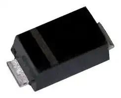
- Diode Mounting: Surface Mount
- Diode Case Style: SOD-923
- Clamping Voltage Max: 9.8V
- Reverse Standoff Voltage: 5V
- Maximum Breakdown Voltage: 5.4V
- Minimum Breakdown Voltage: 5.4V
- Operating Temperature Max: 150°C
| Delivery and price | |
|---|---|
| Units per pack | 500 |
| Price | 0.062 € |
| Current stock | 1000+ |
| Lead time | 7 days |
## ESD9L, SESD9L Series

## Transient Voltage Suppressors **ESD Protection Diodes with Ultra−Low Capacitance**

The ESD9L Series is designed to protect voltage sensitive components that require ultra−low capacitance from ESD and transient voltage events. Excellent clamping capability, low capacitance, low leakage, and fast response time, make these parts ideal for ESD protection on designs where board space is at a premium. Because of its low capacitance, it is suited for use in high frequency designs such as USB 2.0 high speed and antenna line applications.

## **Specification Features:**

- Ultra Low Capacitance 0.5 pF

- Low Clamping Voltage

- Small Body Outline Dimensions: 0.039″ x 0.024″ (1.00 mm x 0.60 mm)

- Low Body Height: 0.016″ (0.4 mm)

**==> picture [100 x 153] intentionally omitted <==**

**----- Start of picture text -----**<br>
www.onsemi.com<br>1 2<br>o—\¢—_o<br>PIN 1. CATHODE<br>2. ANODE<br>2<br>©<br>1<br>SOD−923<br>CASE 514AB<br>**----- End of picture text -----**<br>


- Stand−off Voltage: 3.3 V, 5 V

- Low Leakage

- Response Time is Typically < 1.0 ns

## **MARKING DIAGRAM**

- IEC61000−4−2 Level 4 ESD Protection

- S and SZ Prefixes for Automotive and Other Applications Requiring Unique Site and Control Change Requirements; AEC−Q101 Qualified and PPAP Capable

- These Devices are Pb−Free and are RoHS Compliant

## **Mechanical Characteristics:**

> **CASE:** Void-free, transfer-molded, thermosetting plastic Epoxy Meets UL 94 V−0 **LEAD FINISH:** 100% Matte Sn (Tin)

## **MOUNTING POSITION:** Any **QUALIFIED MAX REFLOW TEMPERATURE:** 260°C

Device Meets MSL 1 Requirements

## **MAXIMUM RATINGS**

|**MAXIMUM RATINGS**||||
|---|---|---|---|
|**Rating**|**Symbol**|**Value**|**Unit**|
|IEC 61000−4−2 (ESD)<br>Contact<br>Air||±10<br>±15|kV|
|Total Power Dissipation on FR−5 Board<br>(Note 1) @ TA= 25°C|°PD°|150|mW|
|Storage Temperature Range|Tstg|−55 to +150|°C|
|Junction Temperature Range|TJ|−55 to +150|°C|
|Lead Solder Temperature − Maximum<br>(10 Second Duration)|TL|260|°C|


Stresses exceeding those listed in the Maximum Ratings table may damage the device. If any of these limits are exceeded, device functionality should not be assumed, damage may occur and reliability may be affected.

**==> picture [98 x 44] intentionally omitted <==**

**----- Start of picture text -----**<br>
1 X M 2<br>X = Specific Device Code<br>M = Date Code<br>**----- End of picture text -----**<br>


*Date Code orientation and/or position may vary depending upon manufacturing location.

## **ORDERING INFORMATION**

|**Device**|**Package**|**Shipping**†|
|---|---|---|
|ESD9LxxxST5G|SOD−923<br>(Pb−Free)|8000/Tape & Reel|
|SESD9LxxxST5G|SOD−923<br>(Pb−Free)|8000/Tape & Reel|
|SZESD9LxxxST5G|SOD−923<br>(Pb−Free)|8000/Tape & Reel|


- †For information on tape and reel specifications, including part orientation and tape sizes, please refer to our Tape and Reel Packaging Specifications Brochure, BRD8011/D.

## **DEVICE MARKING INFORMATION**

See specific marking information in the device marking column of the Electrical Characteristics tables starting on page 2 of this data sheet.

1. FR−5 = 1.0 x 0.75 x 0.62 in.

See Application Note AND8308/D for further description of survivability specs.

Publication Order Number: **ESD9L/D**

**1**

© Semiconductor Components Industries, LLC, 2017 **January, 2017 − Rev. 6**

**ESD9L, SESD9L Series**

## **ELECTRICAL CHARACTERISTICS**

## (TA = 25 ° C unless otherwise noted)

|(TA = 25A = 25= 25C unless otherwise noted)|C unless otherwise noted)|||||||**I**||||
|---|---|---|---|---|---|---|---|---|---|---|---|
|**Symbol**|**Parameter**||||||IF|||||
|IPP|Maximum Reverse Peak Pulse Current|||||||||||
|VC|Clamping Voltage @ IPP||||||||||||
|VRWM|Working Peak Reverse Voltage||||||||||||
|IR<br>VBR|Maximum Reverse Leakage Current @ VRWM<br>Breakdown Voltage @ IT||VRWM<br>VC VBR<br>||||||IR<br>IT|VF||**V**|
|IT|Test Current|||<br>||||||||||
|IF|Forward Current||||||||||||
|VF|Forward Voltage @ IF|||||||IPP||||
|Ppk|Peak Power Dissipation|||||||||||
|C|Max. Capacitance @ VR= 0 and f = 1.0 MHz|||||**Uni−Directional TVS**||||||


- *See Application Note AND8308/D for detailed explanations of datasheet parameters.

## **ELECTRICAL CHARACTERISTICS** (TA = 25 ° C unless otherwise noted, VF = 1.0 V Max. @ IF = 10 mA for all types)

|**Device***|**Device**<br>**Marking**|**VRWM**<br>**(V)**|**IR ( A)**<br>**@ VRWM**|**VBR (V) @ IT**<br>**(Note 2)**|**IT**|**C (pF)**|**C (pF)**|**VC (V)**<br>**@ IPP = 1 A**|**VC**|
|---|---|---|---|---|---|---|---|---|---|
|||**Max**|**Max**|**Min**|**mA**|**Typ**|**Max**|**Max**|**Per IEC61000−4−2**<br>**(Note 4)**|
|ESD9L3.3ST5G|6**|3.3|1.0|4.8|1.0|0.5|0.9|9.0|Figures 1 and 2<br>See Below|
|ESD9L5.0ST5G|D|5.0|1.0|5.4|1.0|0.5|0.9|9.8|Figures 1 and 2<br>See Below|


* Includes S and SZ-prefix devices where applicable.

° **Rotated 180 .

2. VBR is measured with a pulse test current IT at an ambient temperature of 25 ° C.

3. Surge current waveform per Figure 5.

4. For test procedure see Figures 3 and 4 and Application Note AND8307/D.

**Figure 1. ESD Clamping Voltage Screenshot Positive 8 kV Contact per IEC61000−4−2**

**Figure 2. ESD Clamping Voltage Screenshot Negative 8 kV Contact per IEC61000−4−2**

**www.onsemi.com**

**2**

**ESD9L, SESD9L Series**

## **IEC 61000−4−2 Spec.**

|**Level**|**Test Volt-**<br>**age (kV)**|**First Peak**<br>**Current**<br>**(A)**|**Current at**<br>**30 ns (A)**|**Current at**<br>**60 ns (A)**|
|---|---|---|---|---|
|1|2|7.5|4|2|
|2|4|15|8|4|
|3|6|22.5|12|6|
|4|8|30|16|8|


**==> picture [231 x 156] intentionally omitted <==**

**----- Start of picture text -----**<br>
IEC61000−4−2 Waveform<br>Ipeak<br>100%<br>90%<br>I @ 30 ns<br>I @ 60 ns<br>10%<br>tP = 0.7 ns to 1 ns<br>**----- End of picture text -----**<br>


**Figure 3. IEC61000−4−2 Spec**

**==> picture [441 x 120] intentionally omitted <==**

**----- Start of picture text -----**<br>
ESD Gun Oscilloscope<br>TVS<br>50  �<br>Cable 50  �<br>**----- End of picture text -----**<br>


**Figure 4. Diagram of ESD Test Setup**

## **The following is taken from Application Note AND8308/D − Interpretation of Datasheet Parameters for ESD Devices.**

## **ESD Voltage Clamping**

For sensitive circuit elements it is important to limit the voltage that an IC will be exposed to during an ESD event to as low a voltage as possible. The ESD clamping voltage is the voltage drop across the ESD protection diode during an ESD event per the IEC61000−4−2 waveform. Since the IEC61000−4−2 was written as a pass/fail spec for larger

systems such as cell phones or laptop computers it is not clearly defined in the spec how to specify a clamping voltage at the device level. ON Semiconductor has developed a way to examine the entire voltage waveform across the ESD protection diode over the time domain of an ESD pulse in the form of an oscilloscope screenshot, which can be found on the datasheets for all ESD protection diodes. For more information on how ON Semiconductor creates these screenshots and how to interpret them please refer to AND8307/D.

**==> picture [237 x 168] intentionally omitted <==**

**----- Start of picture text -----**<br>
100<br>tr PEAK VALUE IRSM @ 8 �s<br>90<br>80 PULSE WIDTH (tP) IS DEFINED<br>AS THAT POINT WHERE THE<br>70 PEAK CURRENT DECAY = 8 �s<br>60<br>HALF VALUE IRSM/2 @ 20 �s<br>50<br>40<br>30<br>tP<br>20<br>10<br>0<br>0 20 40 60 80<br>t, TIME ( � s)<br>% OF PEAK PULSE CURRENT<br>**----- End of picture text -----**<br>


**Figure 5. 8 X 20 � s Pulse Waveform**

**www.onsemi.com**

**3**

**ESD9L, SESD9L Series**

## **PACKAGE DIMENSIONS**

**SOD−923** CASE 514AB ISSUE C

**==> picture [145 x 247] intentionally omitted <==**

**----- Start of picture text -----**<br>
−X−<br>D<br>−Y−<br>E<br>1 2<br>2X b +qhy<br>0.08 X Y<br>TOP VIEW<br>A<br>c ,taou HE t<br>SIDE VIEW<br>2X L<br>2X L2 fee<br>BOTTOM VIEW<br>**----- End of picture text -----**<br>


NOTES:

1. DIMENSIONING AND TOLERANCING PER ASME Y14.5M, 1994.

2. CONTROLLING DIMENSION: MILLIMETERS.

3. MAXIMUM LEAD THICKNESS INCLUDES LEAD FINISH. MINIMUM LEAD THICKNESS IS THE MINIMUM THICKNESS OF BASE MATERIAL.

**==> picture [152 x 94] intentionally omitted <==**

**----- Start of picture text -----**<br>
4. DIMENSIONS D AND E DO NOT INCLUDE MOLD<br>FLASH, PROTRUSIONS, OR GATE BURRS.<br>MILLIMETERS INCHES<br>DIM MIN NOM MAX MIN NOM MAX<br>A 0.34 0.37 0.40 0.013 0.015 0.016<br>b 0.15 0.20 0.25 0.006 0.008 0.010<br>c 0.07 0.12 0.17 0.003 0.005 0.007<br>D 0.75 0.80 0.85 0.030 0.031 0.033<br>E 0.55 0.60 0.65 0.022 0.024 0.026<br>HE 0.95 1.00 1.05 0.037 0.039 0.041<br>L 0.19 REF 0.007 REF<br>{======<br>L2 0.05 0.10 0.15 0.002 0.004 0.006<br>foefa a<br>**----- End of picture text -----**<br>


## **SOLDERING FOOTPRINT***

**==> picture [118 x 72] intentionally omitted <==**

**----- Start of picture text -----**<br>
1.20<br>2X<br>0.36 2X<br>0.25<br>PACKAGE bs<br>OUTLINE<br>DIMENSIONS: MILLIMETERS<br>**----- End of picture text -----**<br>


See Application Note AND8455/D for more mounting details

*For additional information on our Pb−Free strategy and soldering details, please download the ON Semiconductor Soldering and Mounting Techniques Reference Manual, SOLDERRM/D.

ON Semiconductor and      are trademarks of Semiconductor Components Industries, LLC dba ON Semiconductor or its subsidiaries in the United States and/or other countries. ON Semiconductor owns the rights to a number of patents, trademarks, copyrights, trade secrets, and other intellectual property. A listing of ON Semiconductor’s product/patent coverage may be accessed at www.onsemi.com/site/pdf/Patent−Marking.pdf. ON Semiconductor reserves the right to make changes without further notice to any products herein. ON Semiconductor makes no warranty, representation or guarantee regarding the suitability of its products for any particular purpose, nor does ON Semiconductor assume any liability arising out of the application or use of any product or circuit, and specifically disclaims any and all liability, including without limitation special, consequential or incidental damages. Buyer is responsible for its products and applications using ON Semiconductor products, including compliance with all laws, regulations and safety requirements or standards, regardless of any support or applications information provided by ON Semiconductor. “Typical” parameters which may be provided in ON Semiconductor data sheets and/or specifications can and do vary in different applications and actual performance may vary over time. All operating parameters, including “Typicals” must be validated for each customer application by customer’s technical experts. ON Semiconductor does not convey any license under its patent rights nor the rights of others. ON Semiconductor products are not designed, intended, or authorized for use as a critical component in life support systems or any FDA Class 3 medical devices or medical devices with a same or similar classification in a foreign jurisdiction or any devices intended for implantation in the human body. Should Buyer purchase or use ON Semiconductor products for any such unintended or unauthorized application, Buyer shall indemnify and hold ON Semiconductor and its officers, employees, subsidiaries, affiliates, and distributors harmless against all claims, costs, damages, and expenses, and reasonable attorney fees arising out of, directly or indirectly, any claim of personal injury or death associated with such unintended or unauthorized use, even if such claim alleges that ON Semiconductor was negligent regarding the design or manufacture of the part. ON Semiconductor is an Equal Opportunity/Affirmative Action Employer. This literature is subject to all applicable copyright laws and is not for resale in any manner.

## **PUBLICATION ORDERING INFORMATION**

**LITERATURE FULFILLMENT** : **N. American Technical Support** : 800−282−9855 Toll Free **ON Semiconductor Website** : **www.onsemi.com** Literature Distribution Center for ON Semiconductor USA/Canada 19521 E. 32nd Pkwy, Aurora, Colorado 80011 USA **Europe, Middle East and Africa Technical Support: Order Literature** : http://www.onsemi.com/orderlit **Phone** : 303−675−2175 or 800−344−3860 Toll Free USA/Canada Phone: 421 33 790 2910 **Fax** : 303−675−2176 or 800−344−3867 Toll Free USA/Canada **Japan Customer Focus Center** For additional information, please contact your local **Email** : orderlit@onsemi.com Phone: 81−3−5817−1050 Sales Representative

## **LITERATURE FULFILLMENT** :

◊

**www.onsemi.com**

**ESD9L/D**

**4**
Updated at February 9, 2023
onsemi is a premier global supplier of intelligent power and sensing technologies, driving disruptive innovations across the automotive, industrial, and cloud infrastructure markets. Recognized for their commitment to sustainability and reliable supply chains, the company accelerates advancements in vehicle electrification, industrial automation, and 5G networks by solving the industry's most complex design challenges. At the core of their portfolio is an industry-leading selection of discrete semiconductors. This extensive range features thousands of high-performance bipolar transistors, single and dual MOSFETs, and a comprehensive array of diodes, including Zener, Schottky, and fast-recovery rectifiers. Engineered for superior thermal performance and energy efficiency, these foundational components are critical for demanding power conversion, switching, and signal conditioning applications. Beyond essential discretes, onsemi provides a robust suite of advanced power management and circuit protection solutions. Their lineup includes intelligent power modules, single IGBTs, and transient voltage suppression (TVS) diodes designed to safeguard sensitive circuitry. Complimented by integrated passive filters, AC/DC LED driver ICs, and specialized sub-2.4GHz RF transceivers, onsemi equips engineers with the scalable, high-quality technologies needed to build a cleaner, smarter, and more connected world.
About Novapart
Novapart is a B2B electronic component broker specialising in stock shortages and cost reduction. We source hard-to-find parts and identify compliant alternatives across a catalogue of 410,000+ components from 500+ manufacturers.
Learn more →Stock Shortage Specialist
When a component is unavailable, discontinued or has an unacceptable lead time, we tap into our network of vetted European and Asian distributors to source what you need — without compromising on quality or traceability.
Request a quote →Compliant Alternatives
We identify pin-to-pin, electrically equivalent substitutes that meet the same certifications (RoHS, AEC-Q100, REACH) as your original specification — validated against datasheets, not just part numbers. Often at a lower cost.
BOM Analysis service →