
Image not available
Illustrative purposes only

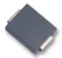
ES3C-13-F
Fast / Ultrafast Diode, 150 V, 3 A, Single, 900 mV, 25 ns, 100 A
⚠️ Reference pricing provided. In case of supply shortages, we will connect you with our trusted procurement partners to ensure your project's continuity.
- Manufacturer: DIODES INC.
- Product type: Fast & Ultrafast Recovery Rectifier Diodes
- SVHC: Lead (25-Jun-2025)
- No. of Pins: 2 Pin
- Product Range: -
- Qualification: -
- Diode Case Style: DO-214AB (SMC)
- Diode Configuration: Single
- Forward Voltage Max: 900mV
- Forward Surge Current: 100A
- Reverse Recovery Time: 25ns
- Average Forward Current: 3A
- Operating Temperature Max: 150°C
- Repetitive Peak Reverse Voltage: 150V
| Delivery and price | |
|---|---|
| Units per pack | 1000 |
| Price | 0.375 € |
| Current stock | 1000+ |
| Lead time | 30 days |
Datasheet

**ES3A/AB - ES3D/DB** **==> picture [19 x 5] intentionally omitted <==** **----- Start of picture text -----**<br> Green<br>**----- End of picture text -----**<br> ## **3.0A SURFACE MOUNT SUPER-FAST RECTIFIER** ## **Features** ## **Mechanical Data** - Glass Passivated Die Construction - Super-Fast Recovery Time for High Efficiency - Surge Overload Rating to 100A Peak - Ideally Suited for Automated Assembly - **Lead-Free Finish; RoHS Compliant (Notes 1 & 2)** - **Halogen and Antimony Free. “Green” Device (Note 3)** - **For automotive applications requiring specific change control (i.e. parts qualified to AEC-Q100/101/200, PPAP capable, and manufactured in IATF 16949 certified facilities), please contact us or your local Diodes representative. https://www.diodes.com/quality/product-definitions/** - Case: SMB/SMC - Case Material: Molded Plastic. UL Flammability Classification Rating 94V-0 - Moisture Sensitivity: Level 1 per J-STD-020 - Terminals: Lead Free Plating (Matte Tin Finish). Solderable per MIL-STD-202, Method 208 - Polarity: Cathode Band or Cathode Notch - SMB Weight: 0.093 grams (Approximate) - SMC Weight: 0.21 grams (Approximate) **==> picture [107 x 8] intentionally omitted <==** **----- Start of picture text -----**<br> Top View Bottom View<br>**----- End of picture text -----**<br> ## **Ordering Information** (Note 4) |**Ordering Informationg Information Information** (Note 4)||| |---|---|---| |**Part Number**|**Case**|**Packaging**| |ES3x-13-F|SMC|3000/Tape & Reel| |ES3xB-13-F|SMB|3000/Tape &Reel| - x = Device type, e.g. ES3A-13-F (SMC package); ES3AB-13-F (SMB package). - Notes: 1. EU Directive 2002/95/EC (RoHS), 2011/65/EU (RoHS 2) & 2015/863/EU (RoHS 3) compliant. All applicable RoHS exemptions applied. 2. See https://www.diodes.com/quality/lead-free/ for more information about Diodes Incorporated’s definitions of Halogen- and Antimony-free, "Green" and Lead-free. 3. Halogen- and Antimony-free "Green” products are defined as those which contain <900ppm bromine, <900ppm chlorine (<1500ppm total Br + Cl) and <1000ppm antimony compounds. 4. For packaging details, go to our website at https://www.diodes.com/design/support/packaging/diodes-packaging/. ## **Marking Information** **SMB SMC** ES3x = Product Type Marking Code, ex: ES3A (SMC Package) ES3xB = Product Type Marking Code, ex: ES3AB (SMB Package) = Manufacturers’ Code Marking YWW = Date Code Marking Y = Last Digit of Year (ex: 0 for 2020) 51: WW = Week Code (01 to 53) 1 of 6 **www.diodes.com** ES3A/AB - ES3D/DB Document number: DS14003 Rev. 16 - 2 February 2020 © Diodes Incorporated **ES3A/AB - ES3D/DB** ## **Maximum Ratings** (@TA = +25°C, unless otherwise specified.) |Single phase, half wave, 60Hz, resistive or inductive load.<br>Forcapacitiveload, derate current by20%.||||||| |---|---|---|---|---|---|---| |**Characteristic**|**Symbol**|**ES3A/AB**|**ES3B/BB**|**ES3C/CB**|**ES3D/DB**|**Unit**| |Peak Repetitive Reverse Voltage<br>Working Peak Reverse Voltage<br>DC Blocking Voltage (Note 5)|VRRM<br>VRWM<br>VR|50|100|150|200|V| |RMS Reverse Voltage|VR(RMS)|35|70|105|140|V| |Average Rectified Output Current<br> @TT= +100C|IO|3.0||||A| |Non-Repetitive Peak Forward Surge Current 8.3ms<br>SingleHalfSine-Wave Superimposed on RatedLoad|IFSM|100||||A| ## **Thermal Characteristics** |**Thermal Characteristics**|||| |---|---|---|---| |**Characteristic**|**Symbol**|**Value**|**Unit**| |Typical Thermal Resistance, Junction to Terminal|RJT|10|C/W| |Typical Thermal Resistance, Junction to Ambient (Note 6)|RJA|50|C/W| |Operating and Storage Temperature Range|TJ,TSTG|-55 to +150|C| ## **Electrical Characteristics** (@TA = +25°C, unless otherwise specified.) |**Electrical Characteristics **(@TA = +25°C, unless otherwise specified.)A = +25°C, unless otherwise specified.)= +25°C, unless otherwise specified.)|(@TA = +25°C, unless otherwise specified.)A = +25°C, unless otherwise specified.)= +25°C, unless otherwise specified.)|(@TA = +25°C, unless otherwise specified.)A = +25°C, unless otherwise specified.)= +25°C, unless otherwise specified.)|| |---|---|---|---| |**Characteristic**|**Symbol**|**Value**|**Unit**| |Maximum Forward Voltage @ IF= 3.0A|= 3.0A<br>VFM|0.9|V| |Peak Reverse Current<br>@ TA= +25C<br>at Rated DC BlockingVoltage(Note 5) @TA= +125C|C<br>IRM|10<br>500|A| |Maximum Reverse Recovery Time (Note 7)|tRR|25|ns| |Typical Total Capacitance (Note 8)|CT|45|pF| Notes: 5. Short duration pulse test used to minimize self-heating effect. 6. Unit mounted on PC board with 5.0 mm[2] (0.013 mm thick) copper pads as heat sink. 7. Measured with IF = 0.5A, IR = 1.0A, IRR = 0.25A. See Figure 5. 8. Measured at 1.0MHz and applied reverse voltage of 4.0V DC. **==> picture [203 x 210] intentionally omitted <==** **----- Start of picture text -----**<br> 4<br>NN ote 36<br>3<br>2<br>1<br>0<br>25 50 75 100 125 150 175<br>TT, TERMINAL TEMPERATURE (°C)<br>Fig. 1 Forward Current Derating Curve<br>, AVERAGE RECTIFIED CURRENT (A)<br>IO<br>**----- End of picture text -----**<br> **==> picture [209 x 211] intentionally omitted <==** **----- Start of picture text -----**<br> 10<br>PPTtT7A rr<br>1.0<br>at<br>——<br>a<br>0.1<br>BEE R<br>——<br>TJ = 25°C<br>0.01 AP| 7 | | [i Pulsein Width: 300use<br>0 0.4 0.8 1.2 1.6<br>VF, INSTANTANEOUS FORWARD VOLTAGE (V)<br>Fig. 2 Typical Forward Characteristics<br>F<br>, INSTANTANEOUS FORWARD CURRENT (A)<br>I<br>**----- End of picture text -----**<br> 2 of 6 **www.diodes.com** ES3A/AB - ES3D/DB Document number: DS14003 Rev. 16 - 2 February 2020 © Diodes Incorporated **ES3A/AB - ES3D/DB** eee ## ! munceceorRPORAT E p® **==> picture [229 x 425] intentionally omitted <==** **----- Start of picture text -----**<br> 120<br>Single Half-Sine-Wave<br>100<br>80 N<br>60 N Z<br>40<br>20<br>0<br>1 10 100<br>NUMBER OF CYCLES AT 60Hz<br>Fig. 3 Surge Current Derating Curve<br>Device<br>() Test<br>"=z Approxvse Generator (Note 10) re<br>oo<br>(Note 9)<br>"<br>Notes:<br>9. Rise Time = 7.0ns max. Input Impedance = 1.0MQ, 22pF.<br>10. Rise Time = 10ns max. Input Impedance = 50Q.<br>, PEAK FORWARD SURGE CURRENT (A)<br>IFSM<br>**----- End of picture text -----**<br> **==> picture [223 x 212] intentionally omitted <==** **----- Start of picture text -----**<br> 1,000<br>—<br>a A<br>a Oa |<br>TJ = 125°C<br>100<br>_—————acees SS SS<br>a eeee<br>10<br>eS aa ES SSSSSS A<br>TJ = 25°C<br>1.0<br>0 40 80 120<br>PERCENT OF RATED PEAK REVERSE VOLTAGE (%)<br>Fig. 4 Typical Reverse Characteristics<br>R<br>, INSTANTANEOUS REVERSE CURRENT (µA)<br>I<br>**----- End of picture text -----**<br> **==> picture [10 x 6] intentionally omitted <==** **----- Start of picture text -----**<br> tRR<br>**----- End of picture text -----**<br> Fig. 5 Reverse Recovery Time Characteristic and Test Circuit 3 of 6 **www.diodes.com** ES3A/AB - ES3D/DB Document number: DS14003 Rev. 16 - 2 February 2020 © Diodes Incorporated **ES3A/AB - ES3D/DB** ## **Package Outline Dimensions** Please see http://www.diodes.com/package-outlines.html for the latest version. ## **SMB** **==> picture [136 x 188] intentionally omitted <==** **----- Start of picture text -----**<br> oo E1<br>D b<br>|Ooos<br>c<br>A<br>L A1<br>E<br>**----- End of picture text -----**<br> **==> picture [86 x 107] intentionally omitted <==** **----- Start of picture text -----**<br> SMB<br>Dim Min Max<br>A 2.00 2.50<br>A1 0.05 0.20<br>b 1.96 2.21<br>c 0.15 0.31<br>D 3.30 3.94<br>E 5.00 5.59<br>E1 4.06 4.57<br>L 0.76 1.52<br>All Dimensions in mm<br>**----- End of picture text -----**<br> ## **SMC** **==> picture [127 x 157] intentionally omitted <==** **----- Start of picture text -----**<br> B<br>-— —+4<br>A C<br>(| bo ta<br>o s n s D<br>J<br>—<br>H G<br>E<br>on<br>**----- End of picture text -----**<br> **==> picture [87 x 106] intentionally omitted <==** **----- Start of picture text -----**<br> SMC<br>Dim Min Max<br>A 5.59 6.22<br>B 6.60 7.11<br>C 2.75 3.18<br>D 0.15 0.31<br>E 7.75 8.13<br>G 0.10 0.20<br>H 0.76 1.52<br>J 2.00 2.50<br>All Dimensions in mm<br>**----- End of picture text -----**<br> 4 of 6 **www.diodes.com** ES3A/AB - ES3D/DB Document number: DS14003 Rev. 16 - 2 February 2020 © Diodes Incorporated **ES3A/AB - ES3D/DB** ## **Suggested Pad Layout** Please see http://www.diodes.com/package-outlines.html for the latest version. ## **SMB** **==> picture [97 x 117] intentionally omitted <==** **----- Start of picture text -----**<br> X1<br>X i<br>Y<br>G<br>pb- C<br>**----- End of picture text -----**<br> |**Dimensions**|**Value**<br>**(in mm)**| |---|---| |**C**<br>**G**|4.30| |**G**|1.80| |**X**|2.50| |**X1**|6.80| |**Y**|2.30| ## **SMC** **==> picture [146 x 108] intentionally omitted <==** **----- Start of picture text -----**<br> X1<br>X<br>Y<br>Ho<br>G<br>Oe C<br>**----- End of picture text -----**<br> |**Dimensions**|**Value**<br>**(in mm)**| |---|---| |**C**|6.90| |**G**|690<br>4.40| |**X**|2.50| |**X1**|9.40| |**Y**|3.30| 5 of 6 **www.diodes.com** ES3A/AB - ES3D/DB Document number: DS14003 Rev. 16 - 2 February 2020 © Diodes Incorporated **ES3A/AB - ES3D/DB** ## **IMPORTANT NOTICE** DIODES INCORPORATED MAKES NO WARRANTY OF ANY KIND, EXPRESS OR IMPLIED, WITH REGARDS TO THIS DOCUMENT, INCLUDING, BUT NOT LIMITED TO, THE IMPLIED WARRANTIES OF MERCHANTABILITY AND FITNESS FOR A PARTICULAR PURPOSE (AND THEIR EQUIVALENTS UNDER THE LAWS OF ANY JURISDICTION). Diodes Incorporated and its subsidiaries reserve the right to make modifications, enhancements, improvements, corrections or other changes without further notice to this document and any product described herein. Diodes Incorporated does not assume any liability arising out of the application or use of this document or any product described herein; neither does Diodes Incorporated convey any license under its patent or trademark rights, nor the rights of others. Any Customer or user of this document or products described herein in such applications shall assume all risks of such use and will agree to hold Diodes Incorporated and all the companies whose products are represented on Diodes Incorporated website, harmless against all damages. Diodes Incorporated does not warrant or accept any liability whatsoever in respect of any products purchased through unauthorized sales channel. Should Customers purchase or use Diodes Incorporated products for any unintended or unauthorized application, Customers shall indemnify and hold Diodes Incorporated and its representatives harmless against all claims, damages, expenses, and attorney fees arising out of, directly or indirectly, any claim of personal injury or death associated with such unintended or unauthorized application. Products described herein may be covered by one or more United States, international or foreign patents pending. Product names and markings noted herein may also be covered by one or more United States, international or foreign trademarks. This document is written in English but may be translated into multiple languages for reference. Only the English version of this document is the final and determinative format released by Diodes Incorporated. ## **LIFE SUPPORT** Diodes Incorporated products are specifically not authorized for use as critical components in life support devices or systems without the express written approval of the Chief Executive Officer of Diodes Incorporated. As used herein: - A. Life support devices or systems are devices or systems which: 1. are intended to implant into the body, or 2. support or sustain life and whose failure to perform when properly used in accordance with instructions for use provided in the labeling can be reasonably expected to result in significant injury to the user. B. A critical component is any component in a life support device or system whose failure to perform can be reasonably expected to cause the failure of the life support device or to affect its safety or effectiveness. Customers represent that they have all necessary expertise in the safety and regulatory ramifications of their life support devices or systems, and acknowledge and agree that they are solely responsible for all legal, regulatory and safety-related requirements concerning their products and any use of Diodes Incorporated products in such safety-critical, life support devices or systems, notwithstanding any devices- or systems-related information or support that may be provided by Diodes Incorporated. Further, Customers must fully indemnify Diodes Incorporated and its representatives against any damages arising out of the use of Diodes Incorporated products in such safety-critical, life support devices or systems. Copyright © 2020, Diodes Incorporated **www.diodes.com** 6 of 6 **www.diodes.com** ES3A/AB - ES3D/DB Document number: DS14003 Rev. 16 - 2 February 2020 © Diodes Incorporated
Updated at June 4, 2026
About Novapart
Novapart is a B2B electronic component broker specialising in stock shortages and cost reduction. We source hard-to-find parts and identify compliant alternatives across a catalogue of 410,000+ components from 500+ manufacturers.
Learn more →Stock Shortage Specialist
When a component is unavailable, discontinued or has an unacceptable lead time, we tap into our network of vetted European and Asian distributors to source what you need — without compromising on quality or traceability.
Request a quote →Compliant Alternatives
We identify pin-to-pin, electrically equivalent substitutes that meet the same certifications (RoHS, AEC-Q100, REACH) as your original specification — validated against datasheets, not just part numbers. Often at a lower cost.
BOM Analysis service →