
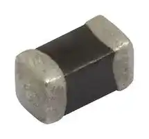


ERTJ0EA220H
NTC THERMISTOR, 22R, 0402
- Manufacturer: PANASONIC
- Product type:
- SVHC: No SVHC (25-Jun-2025)
- B-Constant: 2700K
- Lead Length: -
- NTC Mounting: Surface Mount
- NTC Case Size: 0402 [1005 Metric]
- Product Range: ERTJ Series
- Qualification: -
- Probe Diameter: -
- Probe Material: -
- Thermistor Type: Chip
- Resistance (25°C): 22ohm
- Thermistor Mounting: SMD
- B-Constant Tolerance: ± 3%
- Thermistor Case Style: 0402 [1005 Metric]
- Operating Temperature Max: 125°C
- Operating Temperature Min: -40°C
- Resistance Tolerance (25°C): ± 3%
- Thermal Time Constant (in Air): -
| Delivery and price | |
|---|---|
| Units per pack | 10000 |
| Price | 0.038 € |
| Current stock | 10+ |
| Lead time | 30 days |
**Multilayer NTC Thermistors**

## **Multilayer NTC Thermistors**

## Series: **ERTJ**

## **Features**

- Surface Mount Device (0201, 0402, 0603)

- Highly reliable multilayer / monolithic structure

- Wide temperature operating range (–40 to 125 °C)

- Environmentally-friendly lead-free

- RoHS compliant

## **Recommended Applications**

- Mobile Phone

- Temperature compensation for crystal oscillator

- Temperature compensation for semiconductor devices

- Personal Computer and Peripheral Device

- Temperature detection for CPU and memory device

- Temperature compensation for ink-viscosity (Inkjet Printer)

- Battery Pack (secondary battery)

- Temperature detection of battery cells

- Liquid Crystal Display

- Temperature compensation of display contrast

- Temperature compensation of display backlighting (CCFL)

**==> picture [492 x 355] intentionally omitted <==**

**----- Start of picture text -----**<br>
Explanation of Part Numbers<br>1 2 3 4 5 6 7 8 9 10 11 12<br>E R T J 0 E G 1 0 3 J A (Example)<br>Common Code Size Code Packaging B Value Class Code Nominal Resistance  Resistance Tolerance<br>Product Code Type Code Z “0201” Style Code A 2701 to 2800 R25 (Ω) Code<br>ERT NTC J Chip Type (SMD) 0 “0402” E “0201”, “0402” G 3301 to 3400 The first two digits F ±1% Narrow<br>Thermistors Multilayer Type 1 “0603” Pressed Carrier M 3801 to 3900 are significant figures Tolerance<br>Taping P 4001 to 4100 of resistance and the G ±2% Type<br>Punched Carrier third one denotes<br>Taping R 4201 to 4300 the number of zeros H ±3% Standard<br>(Pitch : 2 mm) S 4301 to 4400 following them. J ±5% Type<br>V “0603” T 4401 to 4500 Special<br>Punched Carrier V 4601 to 4700 Specification<br>Taping<br>esmel (Pitch : 4 mm)<br>Construction<br>No. Name<br>A Semiconductive Ceramics<br>3<br>4 B Internal electrode<br>5 C Substrate electrode<br>2 Terminal<br>1 D Intermediate electrode<br>electrode<br>E External electrode<br>————<br>Design and specifications are each subject to change without notice.  Ask factory for the current technical specifications before purchase and/or use.<br>Should a safety concern arise regarding this product, please be sure to contact us immediately. 05 Dec. 2017<br>**----- End of picture text -----**<br>


**Multilayer NTC Thermistors**

## **Ratings**

|**Ratings**||||
|---|---|---|---|
|Size code (EIA)|Z(0201)|0(0402)|1(0603)|
|Operating Temperature Range||–40 to 125 °C||
|Rated Maximum Power Dissipation✽1|33 mW|66 mW|100 mW|
|DissipationFactor✽2|Approximately<br>1 mW/°C|Approximately<br>2 mW/°C|Approximately<br>3 mW/°C|


- ✽1 Rated Maximum Power Dissipation : The maximum power that can be continuously applied at the rated ambient temperature.

   - The maximum value of power,  and rated power is same under the condition of ambient temperature 25 °C or less. If the temperature exceeds 25 °C, rated power depends on the decreased power dissipation curve.

   - Please see “Operating Power” for details.

- ✽2 Dissipation factor : The constant amount power required to raise the temperature of the Thermistor 1 °C through self heat generation under stable temperatures.

   - Dissipation factor is the reference value when mounted on a glass epoxy board (1.6 mmT).

## **Part Number List of Narrow Tolerance Type** (Resistance Tolerance : ±2 %, ±1 %)

## ● 0201(EIA)

**==> picture [491 x 32] intentionally omitted <==**

**----- Start of picture text -----**<br>
Nominal Resistance Resistance B Value B Value<br>Part Number<br>at 25 °C Tolerance at 25/50(K) at 25/85(K)<br>ERTJZEG103□A  10 kΩ (3380 K) 3435 K±1%<br>**----- End of picture text -----**<br>


|Part Number|Nominal Resistance<br>at 25 °C|Resistance<br>Tolerance|B Value<br>at 25/50(K)|B Value<br>at 25/85(K)|
|---|---|---|---|---|
|ERTJZEG103□A|10 kΩ||(3380 K)|3435 K±1%|
|ERTJZEP473□|47 kΩ|±1 %(F)<br>or<br>±2 %(G)|4050 K±1 %|(4100 K)|
|ERTJZEP683□|68 kΩ||4050 K±1 %|(4100 K)|
|ERTJZER683□|68 kΩ||4250 K±1 %|(4300 K)|
|ERTJZER104□|100 kΩ||4250 K±1 %|(4300 K)|
|ERTJZET104□|100 kΩ||4500 K±1 %|(4550 K)|
|ERTJZEV104□|100 kΩ||4700 K±1 %|(4750 K)|


□ : Resistance Tolerance Code

## ● 0402(EIA)

**==> picture [491 x 31] intentionally omitted <==**

**----- Start of picture text -----**<br>
Nominal Resistance Resistance B Value B Value<br>Part Number<br>at 25 °C Tolerance at 25/50(K) at 25/85(K)<br>ERTJ0EG103□A  10 kΩ (3380 K) 3435 K±1 %<br>**----- End of picture text -----**<br>


|Part Number|Nominal Resistance<br>at 25 °C|Resistance<br>Tolerance|B Value<br>at 25/50(K)|B Value<br>at 25/85(K)|
|---|---|---|---|---|
|ERTJ0EG103□A|10 kΩ||(3380 K)|3435 K±1 %|
|ERTJ0EP333□|33 kΩ|±1 %(F)<br>or<br>±2 %(G)|4050 K±1 %|(4100 K)|
|ERTJ0EP473□|47 kΩ||4050 K±1 %|(4100 K)|
|ERTJ0EP683□|68 kΩ||4050 K±1 %|(4100 K)|
|ERTJ0ER104□|100 kΩ||4250 K±1 %|(4300 K)|
|ERTJ0ES104□|100 kΩ||4330 K±1 %|(4390 K)|
|ERTJ0EV104□|100 kΩ||4700 K±1 %|(4750 K)|
|ERTJ0EV224□|220 kΩ||4700 K±1 %|(4750 K)|


□ : Resistance Tolerance Code

## ● 0603(EIA)

|Part Number|Nominal Resistance<br>at 25 °C|Resistance<br>Tolerance|B Value<br>at 25/50(K)|B Value<br>at 25/85(K)|
|---|---|---|---|---|
|ERTJ1VG103□A|10 kΩ|±1 %(F)<br>or<br>±2 %(G)|(3380 K)|3435 K±1 %|
|ERTJ1VS104□A|100 kΩ||(4330 K)|4390 K±1 %|


□ : Resistance Tolerance Code

## **Part Number List of Standard Type** (Resistance Tolerance : ±5 %, ±3 %)

## ● 0201(EIA)

**==> picture [491 x 32] intentionally omitted <==**

**----- Start of picture text -----**<br>
Nominal Resistance Resistance B Value B Value<br>Part Number<br>at 25 °C Tolerance at 25/50(K) at 25/85(K)<br>ERTJZET202□ 2.0 kΩ 4500 K±2 % (4450 K)<br>**----- End of picture text -----**<br>


|Part Number|Nominal Resistance<br>at 25 °C|Resistance<br>Tolerance|B Value<br>at 25/50(K)|B Value<br>at 25/85(K)|
|---|---|---|---|---|
|ERTJZET202□|2.0 kΩ||4500 K±2 %|(4450 K)|
|ERTJZET302□|3.0 kΩ|±3 %(H)<br>or<br>±5 %(J)|4500 K±2 %|(4450 K)|
|ERTJZET472□|4.7 kΩ||4500 K±2 %|(4450 K)|
|ERTJZEG103□A|10 kΩ||(3380 K)|3435 K±1 %|
|ERTJZEP473□|47 kΩ||4050 K±2 %|(4100 K)|
|ERTJZEP683□|68 kΩ||4050 K±2 %|(4100 K)|
|ERTJZER683□|68 kΩ||4250 K±2 %|(4300 K)|
|ERTJZER104□|100 kΩ||4250 K±2 %|(4300 K)|
|ERTJZET104□|100 kΩ||4500 K±2 %|(4550 K)|
|ERTJZEV104□|100 kΩ||4700 K±2 %|(4750 K)|
|ERTJZET154□|150 kΩ||4500 K±2 %|(4750 K)|
|ERTJZET224□|220 kΩ||4500 K±2 %|(4750 K)|


□ : Resistance Tolerance Code

Design and specifications are each subject to change without notice.  Ask factory for the current technical specifications before purchase and/or use. Should a safety concern arise regarding this product, please be sure to contact us immediately.

05 Dec. 2017

**Multilayer NTC Thermistors**

## ● 0402(EIA)

**==> picture [492 x 24] intentionally omitted <==**

**----- Start of picture text -----**<br>
Nominal Resistance Resistance B Value B Value<br>Part Number<br>at 25 °C Tolerance at 25/50(K) at 25/85(K)<br>**----- End of picture text -----**<br>


|Part Number|Nominal Resistance<br>at 25 °C|Resistance<br>Tolerance|B Value<br>at 25/50(K)|B Value<br>at 25/85(K)|
|---|---|---|---|---|
||||||
|ERTJ0EA220□|22Ω|±3 %(H)<br>or<br>±5 %(J)|2750 K±3 %|(2700 K)|
|ERTJ0EA330□|33Ω||2750 K±3 %|(2700 K)|
|ERTJ0EA400□|40Ω||2750 K±3 %|(2700 K)|
|ERTJ0EA470□|47Ω||2750 K±3 %|(2700 K)|
|ERTJ0EA680□|68Ω||2800 K±3 %|(2750 K)|
|ERTJ0EA101□|100Ω||2800 K±3 %|(2750 K)|
|ERTJ0EA151□|150Ω||2800 K±3 %|(2750 K)|
|ERTJ0ET102□|1.0 kΩ||4500 K±2 %|(4450 K)|
|ERTJ0ET152□|1.5 kΩ||4500 K±2 %|(4450 K)|
|ERTJ0ET202□|2.0 kΩ||4500 K±2 %|(4450 K)|
|ERTJ0ET222□|2.2 kΩ||4500 K±2 %|(4450 K)|
|ERTJ0ET302□|3.0 kΩ||4500 K±2 %|(4450 K)|
|ERTJ0ER332□|3.3 kΩ||4250 K±2 %|(4300 K)|
|ERTJ0ET332□|3.3 kΩ||4500 K±2 %|(4450 K)|
|ERTJ0ET472□|4.7 kΩ||4500 K±2 %|(4450 K)|
|ERTJ0ER472□|4.7 kΩ||4250 K±2 %|(4300 K)|
|ERTJ0ER682□|6.8 kΩ||4250 K±2 %|(4300 K)|
|ERTJ0EG103□A|10 kΩ||(3380 K)|3435 K±1 %|
|ERTJ0EM103□|10 kΩ||3900 K±2 %|(3970 K)|
|ERTJ0ER103□|10 kΩ||4250 K±2 %|(4300 K)|
|ERTJ0ER153□|15 kΩ||4250 K±2 %|(4300 K)|
|ERTJ0ER223□|22 kΩ||4250 K±2 %|(4300 K)|
|ERTJ0EP333□|33 kΩ||4050 K±2 %|(4100 K)|
|ERTJ0ER333□|33 kΩ||4250 K±2 %|(4300 K)|
|ERTJ0ET333□|33 kΩ||4500 K±2 %|(4580 K)|
|ERTJ0EP473□|47 kΩ||4050 K±2 %|(4100 K)|
|ERTJ0ET473□|47 kΩ||4500 K±2 %|(4550 K)|
|ERTJ0EV473□|47 kΩ||4700 K±2 %|(4750 K)|
|ERTJ0EP683□|68 kΩ||4050 K±2 %|(4100 K)|
|ERTJ0ER683□|68 kΩ||4250 K±2 %|(4300 K)|
|ERTJ0EV683□|68 kΩ||4700 K±2 %|(4750 K)|
|ERTJ0EP104□|100 kΩ||4050 K±2 %|(4100 K)|
|ERTJ0ER104□|100 kΩ||4250 K±2 %|(4300 K)|
|ERTJ0ES104□|100 kΩ||4330 K±2 %|(4390 K)|
|ERTJ0ET104□|100 kΩ||4500 K±2 %|(4580 K)|
|ERTJ0EV104□|100 kΩ||4700 K±2 %|(4750 K)|
|ERTJ0ET154□|150 kΩ||4500 K±2 %|(4580 K)|
|ERTJ0EV154□|150 kΩ||4700 K±2 %|(4750 K)|
|ERTJ0EV224□|220 kΩ||4700 K±2 %|(4750 K)|
|ERTJ0EV334□|330 kΩ||4700 K±2 %|(4750 K)|
|ERTJ0EV474□|470 kΩ||4700 K±2 %|(4750 K)|


□ : Resistance Tolerance Code

Design and specifications are each subject to change without notice.  Ask factory for the current technical specifications before purchase and/or use. Should a safety concern arise regarding this product, please be sure to contact us immediately.

05 Dec. 2017

**Multilayer NTC Thermistors**

## ● 0603(EIA)

**==> picture [492 x 24] intentionally omitted <==**

**----- Start of picture text -----**<br>
Nominal Resistance Resistance B Value B Value<br>Part Number<br>at 25 °C Tolerance at 25/50(K) at 25/85(K)<br>**----- End of picture text -----**<br>


|Part Number|Nominal Resistance<br>at 25 °C|Resistance<br>Tolerance|B Value<br>at 25/50(K)|B Value<br>at 25/85(K)|
|---|---|---|---|---|
||||||
|ERTJ1VA220□|22Ω|±3 %(H)<br>or<br>±5 %(J)|2750 K±3 %|(2700 K)|
|ERTJ1VA330□|33Ω||2750 K±3 %|(2700 K)|
|ERTJ1VA400□|40Ω||2800 K±3 %|(2750 K)|
|ERTJ1VA470□|47Ω||2800 K±3 %|(2750 K)|
|ERTJ1VA680□|68Ω||2800 K±3 %|(2750 K)|
|ERTJ1VA101□|100Ω||2800 K±3 %|(2750 K)|
|ERTJ1VT102□|1.0 kΩ||4500 K±2 %|(4450 K)|
|ERTJ1VT152□|1.5 kΩ||4500 K±2 %|(4450 K)|
|ERTJ1VT202□|2.0 kΩ||4500 K±2 %|(4450 K)|
|ERTJ1VT222□|2.2 kΩ||4500 K±2 %|(4450 K)|
|ERTJ1VT302□|3.0 kΩ||4500 K±2 %|(4450 K)|
|ERTJ1VT332□|3.3 kΩ||4500 K±2 %|(4450 K)|
|ERTJ1VR332□|3.3 kΩ||4250 K±2 %|(4300 K)|
|ERTJ1VR472□|4.7 kΩ||4250 K±2 %|(4300 K)|
|ERTJ1VT472□|4.7 kΩ||4500 K±2 %|(4450 K)|
|ERTJ1VR682□|6.8 kΩ||4250 K±2 %|(4300 K)|
|ERTJ1VG103□A|10 kΩ||(3380 K)|3435 K±1%|
|ERTJ1VR103□|10 kΩ||4250 K±2 %|(4300 K)|
|ERTJ1VR153□|15 kΩ||4250 K±2 %|(4300 K)|
|ERTJ1VR223□|22 kΩ||4250 K±2 %|(4300 K)|
|ERTJ1VR333□|33 kΩ||4250 K±2 %|(4300 K)|
|ERTJ1VP473□|47 kΩ||4100 K±2 %|(4150 K)|
|ERTJ1VR473□|47 kΩ||4250 K±2 %|(4300 K)|
|ERTJ1VV473□|47 kΩ||4700 K±2 %|(4750 K)|
|ERTJ1VR683□|68 kΩ||4250 K±2 %|(4300 K)|
|ERTJ1VV683□|68 kΩ||4700 K±2 %|(4750 K)|
|ERTJ1VS104□A|100 kΩ||(4330 K)|4390 K±1%|
|ERTJ1VV104□|100 kΩ||4700 K±2 %|(4750 K)|
|ERTJ1VV154□|150 kΩ||4700 K±2 %|(4750 K)|
|ERTJ1VT224□|220 kΩ||4500 K±2 %|(4580 K)|


□ : Resistance Tolerance Code

Design and specifications are each subject to change without notice.  Ask factory for the current technical specifications before purchase and/or use. Should a safety concern arise regarding this product, please be sure to contact us immediately.

05 Dec. 2017

**Multilayer NTC Thermistors**

> ● Temperature and Resistance value (the resistance value at 25 °C is set to 1)/ Reference values

|● Te|mperature and Resi|mperature and Resi|stance va|lue (the re|sistance|value at 2|5 °C is se|t to 1)/ Re|ference v|alues||
|---|---|---|---|---|---|---|---|---|---|---|---|
||ERTJ□□A~||ERTJ□□G~|ERTJ□□M~|ERTJ□□P~|ERTJ□□R~|ERTJ0ES~|ERTJ1VS~|ERTJ□□T~|ERTJ□□T~|ERTJ□□V~|
|B25/50|2750 K|2800 K|(3375 K)|3900 K|4050 K|4250 K|4330 K|(4330 K)|4500 K|4500 K|4700 K|
|B25/85|(2700 K)|(2750 K)|3435 K|(3970 K)|(4100 K)|(4300 K)|(4390 K)|4390 K|(4450 K)|(4580 K)|(4750 K)|
|T(°C)|||||||||✽1|✽2||
|-40|13.05|13.28|20.52|32.11|33.10|43.10|45.67|45.53|63.30|47.07|59.76|
|-35|10.21|10.40|15.48|23.29|24.03|30.45|32.08|31.99|42.92|33.31|41.10|
|-30|8.061|8.214|11.79|17.08|17.63|21.76|22.80|22.74|29.50|23.80|28.61|
|-25|6.427|6.547|9.069|12.65|13.06|15.73|16.39|16.35|20.53|17.16|20.14|
|-20|5.168|5.261|7.037|9.465|9.761|11.48|11.91|11.89|14.46|12.49|14.33|
|-15|4.191|4.261|5.507|7.147|7.362|8.466|8.743|8.727|10.30|9.159|10.31|
|-10|3.424|3.476|4.344|5.444|5.599|6.300|6.479|6.469|7.407|6.772|7.482|
|-5|2.819|2.856|3.453|4.181|4.291|4.730|4.845|4.839|5.388|5.046|5.481|
|0|2.336|2.362|2.764|3.237|3.312|3.582|3.654|3.650|3.966|3.789|4.050|
|5|1.948|1.966|2.227|2.524|2.574|2.734|2.778|2.776|2.953|2.864|3.015|
|10|1.635|1.646|1.806|1.981|2.013|2.102|2.128|2.126|2.221|2.179|2.262|
|15|1.380|1.386|1.474|1.567|1.584|1.629|1.642|1.641|1.687|1.669|1.710|
|20|1.171|1.174|1.211|1.247|1.255|1.272|1.277|1.276|1.293|1.287|1.303|
|25|1|1|1|1|1|1|1|1|1|1|1|
|30|0.8585|0.8565|0.8309|0.8072|0.8016|0.7921|0.7888|0.7890|0.7799|0.7823|0.7734|
|35|0.7407|0.7372|0.6941|0.6556|0.6461|0.6315|0.6263|0.6266|0.6131|0.6158|0.6023|
|40|0.6422|0.6376|0.5828|0.5356|0.5235|0.5067|0.5004|0.5007|0.4856|0.4876|0.4721|
|45|0.5595|0.5541|0.4916|0.4401|0.4266|0.4090|0.4022|0.4025|0.3874|0.3884|0.3723|
|50|0.4899|0.4836|0.4165|0.3635|0.3496|0.3319|0.3251|0.3254|0.3111|0.3111|0.2954|
|55|0.4309|0.4238|0.3543|0.3018|0.2881|0.2709|0.2642|0.2645|0.2513|0.2504|0.2356|
|60|0.3806|0.3730|0.3027|0.2518|0.2386|0.2222|0.2158|0.2161|0.2042|0.2026|0.1889|
|65|0.3376|0.3295|0.2595|0.2111|0.1985|0.1832|0.1772|0.1774|0.1670|0.1648|0.1523|
|70|0.3008|0.2922|0.2233|0.1777|0.1659|0.1518|0.1463|0.1465|0.1377|0.1348|0.1236|
|75|0.2691|0.2600|0.1929|0.1504|0.1393|0.1264|0.1213|0.1215|0.1144|0.1108|0.1009|
|80|0.2417|0.2322|0.1672|0.1278|0.1174|0.1057|0.1011|0.1013|0.09560|0.09162|0.08284|
|85|0.2180|0.2081|0.1451|0.1090|0.09937|0.08873|0.08469|0.08486|0.08033|0.07609|0.06834|
|90|0.1974|0.1871|0.1261|0.09310|0.08442|0.07468|0.07122|0.07138|0.06782|0.06345|0.05662|
|95|0.1793|0.1688|0.1097|0.07980|0.07200|0.06307|0.06014|0.06028|0.05753|0.05314|0.04712|
|100|0.1636|0.1528|0.09563|0.06871|0.06166|0.05353|0.05099|0.05112|0.04903|0.04472|0.03939|
|105|0.1498|0.1387|0.08357|0.05947|0.05306|0.04568|0.04340|0.04351|0.04198|0.03784|0.03308|
|110|0.1377|0.1263|0.07317|0.05170|0.04587|0.03918|0.03708|0.03718|0.03609|0.03218|0.02791|
|115|0.1270|0.1153|0.06421|0.04512|0.03979|0.03374|0.03179|0.03188|0.03117|0.02748|0.02364|
|120|0.1175|0.1056|0.05650|0.03951|0.03460|0.02916|0.02734|0.02742|0.02702|0.02352|0.02009|
|125|0.1091|0.09695|0.04986|0.03470|0.03013|0.02527|0.02359|0.02367|0.02351|0.02017|0.01712|


✽1 Apply to products with a B[25/50] constant of 4500 K and a resistance value of 25 °C less than 10 kΩ. ✽2 Applied only to ERTJ0ET104□.

✽2 Apply to products with a B[25/50] constant of 4500 K and a resistance value of 25 °C of 10 kΩ or more. ✽2 Applied only to ERTJ0ET104□.

**==> picture [385 x 27] intentionally omitted <==**

Design and specifications are each subject to change without notice.  Ask factory for the current technical specifications before purchase and/or use. Should a safety concern arise regarding this product, please be sure to contact us immediately.

05 Dec. 2017

**Multilayer NTC Thermistors**

## **Specifi cation and Test Method**

**==> picture [491 x 566] intentionally omitted <==**

**----- Start of picture text -----**<br>
Item Specifi cation Test Method<br>Rated Zero-power  Within the specifi ed tolerance. The value is measured at a power that the infl uence<br>Resistance (R25) of self-heat generation can be negligible (0.1mW or<br>less), at the rated ambient temperature of 25.0±0.1°C.<br>B Value Shown in each Individual Specifi cation. The Zero-power resistances; R1 and R2, shall be<br>✽ Individual Specifi cation shall specify B [25/50]  or  measured respectively at T1 (deg.C) and T2 (deg.C).<br>B25/85. The B value is calculated by the following equation.<br>kn  (R [1] )–kn  (R [2] )<br>BT1/T2=<br>1/(T1+273.15)–1/(T2+273.15)<br>T1 T2<br>B25/50 25.0 ±0.1 °C 50.0 ±0.1 °C<br>B25/85 25.0 ±0.1 °C 85.0 ±0.1 °C<br>Adhesion The terminal electrode shall be free from peeling  Applied force :<br>or signs of peeling. Size 0201  : 2 N<br>Size 0402, 0603 : 5 N<br>Duration : 10 s<br>Size : 0201, 0402<br>0.3/Size:0201<br>1.0 0.5R 0.5/Size:0402<br>Test Sample Board<br>Size : 0603<br>Test<br>Sample Unit : mm<br>Bending Strength There shall be no cracks and other mechanical  Bending distance : 1 mm<br>damage. Bending speed  : 1 mm/s<br>R25 change : within ±5 %<br>20<br>R340<br>45±2 45±2<br>Unit : mm<br>Resistance to  There shall be no cracks and other mechanical  Soldering bath method<br>Soldering Heat damage. Solder temperature : 270 ±5 °C<br> Nallow Tol. type Standard type Dipping period  : 4.0 ±1 s<br>R25 change  :  within ±2 %  within ±3 % Preheat condition  :<br>B Value change :  within ±1 %  within ±2 % Step Temp (°C) Period (s)<br>1  80 to 100 120 to 180<br>2 150 to 200 120 to 180<br>Solderability More than 95 % of the soldered area of both  Soldering bath method<br>terminal electrodes shall be covered with fresh  Solder temperature : 230 ±5 °C<br>solder. Dipping period  : 4 ±1 s<br>Solder  : Sn-3.0Ag-0.5Cu<br>1.0<br>Bendingdistance<br>**----- End of picture text -----**<br>


Design and specifications are each subject to change without notice.  Ask factory for the current technical specifications before purchase and/or use. Should a safety concern arise regarding this product, please be sure to contact us immediately.

05 Dec. 2017

**Multilayer NTC Thermistors**

## **Specifi cation and Test Method**

**==> picture [491 x 15] intentionally omitted <==**

**----- Start of picture text -----**<br>
Item Specifi cation Test Method<br>**----- End of picture text -----**<br>


|Item|Specif cation|Test Method|
|---|---|---|
||||
|Temperature<br>Cycling|Nallow Tol. type Standard type<br>R25change<br>:<br>within ±2 %<br>within ±3 %<br>B Value change :<br>within ±1 %<br>within ±2 %|Conditions of one cycle<br>Step 1 : –40 °C, 30±3 min<br>Step 2 : Room temp., 3 min max.<br>Step 3 : 125 °C, 30±3 min.<br>Step 4 : Room temp., 3 min max.<br>Number of cycles: 100 cycles|
|Humidity|Nallow Tol. type Standard type<br>R25change<br>:<br>within ±2 %<br>within ±3 %<br>B Value change :<br>within ±1 %<br>within ±2 %|Temperature<br>: 85 ±2 °C<br>Relative humidity : 85 ±5 %<br>Test period<br>: 1000 +48/0 h|
|Biased Humidity|Nallow Tol. type Standard type<br>R25change<br>:<br>within ±2 %<br>within ±3 %<br>B Value change :<br>within ±1 %<br>within ±2 %|Temperature<br>: 85 ±2 °C<br>Relative humidity : 85 ±5 %<br>Applied power<br>: 10 mW(D.C.)<br>Test period<br>: 500 +48/0 h|
|Low Temperature<br>Exposure|Nallow Tol. type Standard type<br>R25change<br>:<br>within ±2 %<br>within ±3 %<br>B Value change :<br>within ±1 %<br>within ±2 %|Specimens are soldered on the testing board<br>shown in Fig.2.<br>Temperature<br>: –40 ±3 °C<br>Test period<br>: 1000 +48/0 h|
|High Temperature<br>Exposure|Nallow Tol. type Standard type<br>R25change<br>:<br>within ±2 %<br>within ±3 %<br>B Value change :<br>within ±1 %<br>within ±2 %|Specimens are soldered on the testing board<br>shown in Fig.2.<br>Temperature<br>: 125 ±3 °C<br>Test period<br>: 1000 +48/0 h|


## **Typical Application**

- Temperature Detection

   - Writing current control of HDD

**==> picture [211 x 159] intentionally omitted <==**

**----- Start of picture text -----**<br>
Vcc<br>GMR Head<br>R<br>R L<br>AD<br> converter<br>Rth<br>CPU Interface<br>NTC<br>**----- End of picture text -----**<br>


- Temperature Compensation (Pseudo-linearization) Contrast level control of LCD

- Temperature Compensation (RF circuit)

   - Temperature compensation of TCXO

**==> picture [414 x 131] intentionally omitted <==**

**----- Start of picture text -----**<br>
Vcc PMIC<br>R<br>R<br>LCD<br>NTC<br>Rth R<br>Rth<br>ADC<br>NTC<br>**----- End of picture text -----**<br>


Design and specifications are each subject to change without notice.  Ask factory for the current technical specifications before purchase and/or use. Should a safety concern arise regarding this product, please be sure to contact us immediately.

Dec. 2017

05

**Multilayer NTC Thermistors**

## **Dimensions in mm (not to scale)**

|T<br>||||L<br>L2|||(Unit : mm)|(Unit : mm)|(Unit : mm)|
|---|---|---|---|---|---|---|---|---|---|
||W|||L2||||||
||||||Size Code (EIA)|L|W|T|L1, L2|
||||||Z(0201)|0.60±0.03|0.30±0.03|0.30±0.03|0.15±0.05|
|||||||||||
||||||0(0402)|1.0±0.1|0.50±0.05|0.50±0.05|0.25±0.15|
||||||1(0603)|1.60±0.15|0.8±0.1|0.8±0.1|0.3±0.2|
|||||||||||
||||L1|||||||


## **Packaging Methods**

## ● Standard Packing Quantities

|Size<br>Code|Thickness<br>(mm)<br>K|ind of Taping|Pitch<br>(mm)|Quantity<br>(pcs./reel)|
|---|---|---|---|---|
|Z(0201)|0.3<br>Pre|ssed Carrier Taping|2|15,000|
|0(0402)|0.5<br>Pun<br>0.8|ched Carrier Taping|<br>2|10,000|
|1(0603)|||<br>4|4,000|


- Pitch 2 mm (Pressed Carrier Taping) : Size 0201

|t|t|Feeding hole<br>Chip pocket|Feeding hole<br>Chip pocket|Feeding hole<br>Chip pocket|Feeding hole<br>Chip pocket|Feeding hole<br>Chip pocket|Feeding hole<br>Chip pocket|Feeding hole<br>Chip pocket|Feeding hole<br>Chip pocket|Feeding hole<br>Chip pocket|
|---|---|---|---|---|---|---|---|---|---|---|
|K0||fD0|||||F<br>W<br>E<br>Tape runningdirection||||
|||||||||E|||
||||||A<br>B|||F|||
|||Chip component|||||||||
||||||P1 P2|P0|||||
||||||||||||
|Symb|ol<br>A||B|W<br>F|E<br>P1|P2|P0|fD0|t|K0|
|Dim<br>(mm)|.<br><br>0.36<br>±0.03||0.66<br>±0.03|8.0<br>±0.2 3.5<br>±0.0|0<br>5 1.75<br>±0.10 2.00<br>±0.05|2.00<br>±0.05|4.0<br>±0.1|1.5+0.1<br>0|0.55<br>max.|0.36<br>±0.03|


## ● Pitch 2 mm (Punched Carrier Taping) : Size 0402

|t2|t1|Feeding hole<br>Chip pocket|Feeding hole<br>Chip pocket|Feeding hole<br>Chip pocket|Feeding hole<br>Chip pocket|Feeding hole<br>Chip pocket|Feeding hole<br>Chip pocket|Feeding hole<br>Chip pocket|Feeding hole<br>Chip pocket|Feeding hole<br>Chip pocket|
|---|---|---|---|---|---|---|---|---|---|---|
|||fD0|||||Tape runningdirection<br>F<br>W<br>E||||
|||||||||E|||
||||||A<br>|||F|||
|||Chip component|||B||||||
||||||P1 P2|P0<br>|||||
||||||||||||
|Symb|ol<br>A||B|W<br>F|E<br>P1|P2|P0|fD0|t1|t2|
|Dim<br>(mm)|.<br><br>0.62<br>±0.05||1.12<br>±0.05|8.0<br>±0.2 3.5<br>±0.0|0<br>5 1.75<br>±0.10 2.00<br>±0.05|2.00<br>±0.05|4.0<br>±0.1|1.5+0.1<br>0|0.7<br>max.|1.0<br>max.|


## ● Pitch 4 mm (Punched Carrier Taping) : Size 0603

|t2<br>Chip component<br>Feeding hole<br>Chip pocket<br>fD0<br>P1<br>P2<br>P0<br>Ta<br>B<br>~~A~~<br>t1|t2<br>Chip component<br>Feeding hole<br>Chip pocket<br>fD0<br>P1<br>P2<br>P0<br>Ta<br>B<br>~~A~~<br>t1|t2<br>Chip component<br>Feeding hole<br>Chip pocket<br>fD0<br>P1<br>P2<br>P0<br>Ta<br>B<br>~~A~~<br>t1|t2<br>Chip component<br>Feeding hole<br>Chip pocket<br>fD0<br>P1<br>P2<br>P0<br>Ta<br>B<br>~~A~~<br>t1|t2<br>Chip component<br>Feeding hole<br>Chip pocket<br>fD0<br>P1<br>P2<br>P0<br>Ta<br>B<br>~~A~~<br>t1|t2<br>Chip component<br>Feeding hole<br>Chip pocket<br>fD0<br>P1<br>P2<br>P0<br>Ta<br>B<br>~~A~~<br>t1|t2<br>Chip component<br>Feeding hole<br>Chip pocket<br>fD0<br>P1<br>P2<br>P0<br>Ta<br>B<br>~~A~~<br>t1|pe running direction<br>E<br>F<br>W|pe running direction<br>E<br>F<br>W|pe running direction<br>E<br>F<br>W|pe running direction<br>E<br>F<br>W|pe running direction<br>E<br>F<br>W|
|---|---|---|---|---|---|---|---|---|---|---|---|
||fD0<br>||||||pe running direction<br>E<br>F<br>W|||||
||||||||||E|||
|||||~~A~~|||||F|||
|||||||||||||
||Chip component<br>B|||||||||||
||||||P1<br>P2<br>P|0<br>Ta||||||
|||||||||||||
|Symb|ol<br>A|B||W<br>F|E<br>P1|P2|P0||fD0|t1|t2|
|Dim<br>(mm)|.<br><br>1.0<br>±0.1|1.8<br>±0.1||8.0<br>±0.2 3.5<br>±0.0|0<br>5 1.75<br>±0.10 4.0<br>±0.1|2.00<br>±0.05|4.0<br>±0.1||1.5+0.1<br>0|1.1<br>max.|1.4<br>max.|


## ● Reel for Taping

**==> picture [138 x 97] intentionally omitted <==**

**----- Start of picture text -----**<br>
W1<br>E<br>C<br>D<br>W2<br>A<br>B<br>**----- End of picture text -----**<br>


Symbol fA fB C D E W1 W2 Dim.(mm) 180 –30 60.0+1.00 13.0±0.5 21.0±0.8 2.0±0.5 9.0+1.00 11.4[±1.0]

- Leader Part and Taped End

- Leader part

**==> picture [233 x 137] intentionally omitted <==**

**----- Start of picture text -----**<br>
Top cover tape<br>100 min.<br>Vacant position<br>400 min.<br> Taped end<br>160 min.<br>Vacant position (Unit : mm)<br>**----- End of picture text -----**<br>


## **Minimum Quantity / Packing Unit**

**==> picture [233 x 28] intentionally omitted <==**

**----- Start of picture text -----**<br>
Part Number Minimum Quantity Packing Quantity  Carton<br>(Size) / Packing Unit in Carton L×W×H (mm)<br>**----- End of picture text -----**<br>


|Part Number<br>(Size)<br>M|inimum Quantity<br>/ Packing Unit|Packing Quantity<br>in Carton|Carton<br>L×W×H (mm)|
|---|---|---|---|
|||||
|ERTJZ<br>(0201)|15,000|300,000|250×200×200|
|ERTJ0<br>(0402)|10,000|200,000|250×200×200|
|ERTJ1<br>(0603)|4,000|80,000|250×200×200|


Part No., quantity and country of origin are designated on outer packages in English.

Design and specifications are each subject to change without notice.  Ask factory for the current technical specifications before purchase and/or use. Should a safety concern arise regarding this product, please be sure to contact us immediately.

05 Dec. 2017

Panasonic inoustry

**==> picture [387 x 64] intentionally omitted <==**

**----- Start of picture text -----**<br>
Guidelines and precautions regarding the<br>technical information and use of our products<br>described in this online catalog.<br>**----- End of picture text -----**<br>


m= If you want to use our products described in this online catalog for applications requiring special qualities or reliability, or for applications where the failure or malfunction of the products may directly jeopardize human life or potentially cause personal injury (e.g. aircraft and aerospace equipment, traffic and transportation equipment, combustion equipment, medical equipment, accident prevention, anti-crime equipment, and/or safety equipment), it is necessary to verify whether the specifications of our products fit to such applications. Please ensure that you will ask and check with our inquiry desk as to whether the specifications of our products fit to such applications use before you use our products.

m The quality and performance of our products as described in this online catalog only apply to our products when used in isolation. Therefore, please ensure you evaluate and verify our products under the specific circumstances in which our products are assembled in your own products and in which our products will actually be used.

m@ If you use our products in equipment that requires a high degree of reliability, regardless of the application, it is recommended that you set up protection circuits and redundancy circuits in order to ensure safety of your equipment. m The products and product specifications described in this online catalog are subject to change for improvement without prior notice. Therefore, please be sure to request and confirm the latest product specifications which explain the specifications of our products in detail, before you finalize the design of your applications, purchase, or use our products.

m@ The technical information in this online catalog provides examples of our products' typical operations and application circuits. We do not guarantee the non-infringement of third party's intellectual property rights and we do not grant any license, right, or interest in our intellectual property.

m@ If any of our products, product specifications and/or technical information in this online catalog is to be exported or provided to non-residents, the laws and regulations of the exporting country, especially with regard to security and export control, shall be observed.

<Regarding the Certificate of Compliance with the EU RoHS Directive/REACH Regulations>

m The switchover date for compliance with the RoHS Directive/REACH Regulations varies depending on the part number or series of our products.

m When you use the inventory of our products for which it is unclear whether those products are compliant with the RoHS Directive/REACH Regulation, please select "Sales Inquiry" in the website inquiry form and contact us.

We do not take any responsibility for the use of our products outside the scope of the specifications, descriptions, guidelines and precautions described in this online catalog.

01-Apr-19

**Multilayer NTC Thermistors**

## Multilayer NTC Thermistors Series: ERTJ

## **Handling Precautions**

## **[Precautions]**

- **・ Do not use the products beyond the descriptions in this product catalog.**

- **・ This product catalog guarantees the quality of the products as individual components. Before you use the products, please make sure to check and evaluate the products in the circumstance where they are installed in your product.**

## Safety Precautions

Multilayer NTC Thermistors for General Applications  (hereafter referred to as “Thermistors”) are intended to be used in general-purpose applications as measures against Temperature detection and Temperature compensation in consumer electronics (audio/visual, home, office, information & communication) equipment. When subjected to severe electrical, environmental, and/or mechanical stress beyond the specifications, as noted in the Ratings and Specified Conditions section, the Thermistors’ performance may be degraded, or become failure mode, such as short circuit mode and open-circuit mode.

If you use under the condition of short-circuit, heat generation of Thermistors will occur by running large current due to application of voltage. There are possibilities of smoke emission, substrate burn-out, and, in the worst case, fire.  For products which require high safety levels, please carefully consider how a single malfunction can affect your product. In order to ensure the safety in the case of a single malfunction, please design products with fail-safe, such as setting up protecting circuits, etc.

We are trying to improve the quality and the reliability, but the durability differs depending on the use environment and the use conditions. On use, be sure to confirm the actual product under the actual use conditions.

- For the following applications and conditions, please be sure to consult with our sales representative in advance and to exchange product specifications which conform to such applications.

   - ・ When your application may have difficulty complying with the safety or handling precautions specified below.

   - ・ High-quality and high-reliability required devices that have possibility of causing hazardous conditions, such as death or injury (regardless of directly or indirectly), due to failure or malfunction of the product.

   - ① Aircraft and Aerospace Equipment (artificial satellite, rocket, etc.)

   - ② Submarine Equipment (submarine repeating equipment, etc.)

   - ③ Transportation Equipment (motor vehicles, airplanes, trains, ship, traffic signal controllers, etc.)

   - ④ Power Generation Control Equipment

      - (atomic power, hydroelectric power, thermal power plant control system, etc.)

   - ⑤ Medical Equipment (life-support equipment, pacemakers, dialysis controllers, etc.)

   - ⑥ Information Processing Equipment (large scale computer systems, etc.)

   - ⑦ Electric Heating Appliances, Combustion devices (gas fan heaters, oil fan heaters, etc.)

   - ⑧ Rotary Motion Equipment

   - ⑨ Security Systems

   - ⑩ And any similar types of equipment

## Strict Observance

## **1. Confirmation of Rated Performance**

The Thermistors shall be operated within the specified rating/performance.

Applications exceeding the specifications may cause deteriorated performance and/or breakdown, resulting in degradation and/or smoking or ignition of products. The following are strictly observed.

- (1) The Thermistors shall not be operated beyond the specified operating temperature range.

- (2) The Thermistors shall not be operated in excess of the specified maximum power dissipation.

## **2. The Thermistors shall not be mounted near flammables.**

01. Oct. 2019

**Multilayer NTC Thermistors**

## ~~ee~~ **Operating Conditions and Circuit Design 1. Circuit Design**

## **1.1 Operating Temperature and Storage Temperature**

When operating a components-mounted circuit, please be sure to observe the “Operating Temperature Range”, written in delivery specifications.  Storage temperature of PCB after mounting Thermistors, which is not operated, should be within the specified “Storage Temperature Range” in the delivery specifications. Please remember not to use the product under the condition that exceeds the specified maximum temperature.

## **1.2 Operating Power**

The electricity applied to between terminals of Thermistors should be under the specified maximum power dissipation. There are possibilities of breakage and burn-out due to excessive self-heating of Thermistors, if the power exceeds maximum power dissipation when operating.  Please consider installing protection circuit for your circuit to improve the safety, in case of abnormal voltage application and so on. Thermistors’ performance of temperature detection would be deteriorated if self-heating occurs, even when you use it under the maximum power dissipation. Please consider the maximum power dissipation and dissipation factor.

## **【Maximum power dissipation】**

・The Maximum power that can be continuously applied under static air at a certain ambient temperature. The Maximum power dissipation under an ambient temperature of 25 ℃ or less is the same with the rated maximum power dissipation, and Maximum power dissipation beyond 25 ℃ depends on the Decreased power dissipation curve below.

## **【Dissipation factor】**

- ・The constant amount power required to raise the

temperature of the Thermistor 1 °C through self

**==> picture [196 x 137] intentionally omitted <==**

**----- Start of picture text -----**<br>
Decreased power dissipation curve<br>100<br>50<br>25 75 125<br>Maximum power dissipation / Rated maximum power dissipation (%) Ambient temperature (°C)<br>**----- End of picture text -----**<br>


heat generation under stable temperatures.

- Dissipation factor (mW/°C) = Power consumption

- of Thermistor / Temperature rise of element.

## **1.3 Environmental Restrictions**

The Thermistors does not take the use under the following special environments into consideration. Accordingly, the use in the following special environments, and such environmental conditions may affect the performance of the product; prior to use, verify the performance, reliability, etc. thoroughly.

- ① Use in liquids such as water, oil, chemical, and organic solvent.

- ② Use under direct sunlight, in outdoor or in dusty atmospheres.

- ③ Use in places full of corrosive gases such as sea breeze, Cl2,H2S,NH3,SO2,and NOx.

- ④ Use in environment with large static electricity or strong electromagnetic waves or strong radial ray.

- ⑤ Where the product is close to a heating component, or where an inflammable such as a polyvinyl chloride wire is arranged close to the product.

- ⑥ Where this product is sealed or coated with resin etc.

- ⑦ Where solvent, water, or water-soluble detergent is used in flux cleaning after soldering.

   - (Pay particular attention to water-soluble flux.)

- ⑧ Use in such a place where the product is wetted due to dew condensation.

- ⑨ Use the product in a contaminated state.

   - Ex.) Do not handle the product such as sticking sebum directly by touching the product after mounting printed circuit board.

- ⑩ Under severe conditions of vibration or impact beyond the specified conditions found in the Specifications.

## **1.4 Measurement of Resistance**

The resistance of the Thermistors varies depending on ambient temperatures and self-heating. To measure the resistance value when examining circuit configuration and conducting receiving inspection and so on, the following points should be taken into consideration:

- ① Measurement temp : 25±0.1 °C

Measurement in liquid (silicon oil, etc.) is recommended for a stable measurement temperature.

- ② Power : 0.10 mW max. 4 terminal measurement with a constant-current power supply is recommended.

01. Oct. 2019

**Multilayer NTC Thermistors**

## **2. Design of Printed Circuit Board**

## **2.1 Selection of Printed Circuit Boards**

There is a possibility of performance deterioration by heat shock (temperature cycles), which causes cracks, from alumina substrate. Please confirm that the substrate you use does not deteriorate the Thermistors’ quality. **2.2 Design of Land Pattern**

- (1) Recommended land dimensions are shown below. Use the proper amount of solder in order to prevent cracking.  Using too much solder places excessive stress on the Thermistors..

Recommended Land Dimensions(Ex.)

SMD Land Unit (mm) Size Component dimensions a b c Code/EIA L W T Solder resist Z(0201) 0.6 0.3 0.3 0.2 to 0.3 0.25 to 0.30 0.2 to 0.3 0(0402) 1.0 0.5 0.5 0.4 to 0.5 0.4 to 0.5 0.4 to 0.5 1(0603) 1.6 0.8 0.8 0.8 to 1.0 0.6 to 0.8 0.6 to 0.8 ~~|[|] —~~ (2) The land size shall be designed to have equal space, on both right and left side. If the amount of  solder on both sides is not equal, the component may be cracked by stress since the side  with a larger amount of solder solidifies later during cooling.

## **Recommended Amount of Solder**

(a) Excessive amount (b) Proper amount (c) Insufficient amount

## **2.3 Utilization of Solder Resist**

- (1) Solder resist shall be utilized to equalize the amounts of solder on both sides.

- (2) Solder resist shall be used to divide the pattern for the following cases;

   - ・ Components are arranged closely.

   - ・ The Thermistor is mounted near a component with lead wires.

   - ・ The Thermistor is placed near a chassis.

Refer to the table below.

Prohibited Applications and Recommended Applications

**==> picture [271 x 260] intentionally omitted <==**

**----- Start of picture text -----**<br>
Prohibited Improved applications<br>Item<br>a applications by pattern division<br>Mixed The lead wire of a Component Solder resist<br>mounting With lead wires<br>with a<br>component<br>with lead<br>wires i<br>Chassis<br>Solder resist<br>Arrangement / Solder(ground solder)<br>near<br>chassis<br>=<br>Electrode pattern<br>A lead wire of Retrofitted<br>Retro-fitting component Solder resist<br>of component<br>with lead Solderingiron<br>iron<br>wires at<br>Portion to be<br>Solder resist<br>Excessively soldered<br>Lateral<br>arrangement Land<br>**----- End of picture text -----**<br>


## **2.4 Component Layout**

To prevent the crack of Thermistors,  try to place it place it on the position that could not easily be affected by the bending stress of substrate while mounting procedures or procedures afterwards. Placement of the Thermistors near heating elements also requires the great care to be taken in order to avoid stresses from rapid heating and cooling.

01. Oct. 2019

**Multilayer NTC Thermistors**

**==> picture [317 x 209] intentionally omitted <==**

**----- Start of picture text -----**<br>
Prohibited layout Recommended layout<br>L A<br>L EP _ZA LP __A<br>Layout the Varistors sideways<br>against the stressing direction.<br>E<br>D<br>m 6<br>Perforation<br>C<br>fonenene) [U]<br>Magnitude of stress<br>a ] o0o0o°o [o]<br>A>B=C>D>E<br>A Slit B<br>**----- End of picture text -----**<br>


- (1) To minimize mechanical stress caused by the warp or bending of a PC board, please follow the recommended Thermistors’ layout below.

- (2) The following layout is for your reference since mechanical stress near the dividing/breaking position of a PC board varies depending on the mounting position of the Thermistors.

- (3) The magnitude of mechanical stress applied to the Thermistors when dividing the circuit board in descending order is as follows: push back < slit < V-groove < perforation.  Also take into account the layout of the Thermistors and the dividing/breaking method.

- (4) When the Thermistors are placed near heating elements such as heater, etc., cracks from thermal stresses may occur under following situation:

- ・ Soldering the Thermistors directly to heating elements.

- ・ Sharing the land with heating elements.

If planning to conduct above-mentioned mounting and/or placement, please contact us in advance.

## **2.5 Mounting Density and Spaces**

Intervals between components should not be too narrow to prevent the influence from solder bridges and solder balls. The space between components should be carefully determined.

## ee **Precautions for Assembly**

## **1. Storage**

- (1)  The Thermistors shall be stored between 5 to 40 °C and 20 to 70 % RH, not under severe conditions of high temperature and humidity.

- (2) If stored in a place where humidity, dust, or corrosive gasses (hydrogen sulfide, sulfurous acid, hydrogen chloride and ammonia, etc.) are contained, the solderability of terminals electrodes will be deteriorated. In addition, storage in a place where the heat or direct sunlight exposure occurs will causes or direct sunlight exposure occurs will causes mounting problems due to deformation of tapes and reels and components and taping/reels sticking together.

- (3) Do not store components longer than 6 months. Check the solderability of products that have been stored for more than 6 months before use.

## **2. Chip Mounting Consideration**

- (1) When mounting the Thermistors/components on a PC board, the Thermistor bodies shall be free from excessive impact loads such as mechanical impact or stress due to the positioning, pushing force and displacement of  vacuum nozzles during mounting.

- (2) Maintenance and inspection of the Chip Mounter must be performed regularly.

- (3) If the bottom dead center of the vacuum nozzle is too low, the  Thermistor will crack from excessive force during mounting. The following precautions and recommendations are for your reference in use.

   - (a) Set and adjust the bottom dead center of the vacuum nozzles to the upper surface of the PC board after correcting the warp of the PC board.

   - (b) Set the pushing force of the vacuum nozzle during mounting to 1 to 3 N in static load.

   - (c) For double surface mounting, apply a supporting pin on the rear surface of the PC board to suppress the bending of the PC board in order to minimize the impact of the vacuum nozzles. Typical examples are shown in the table below.

   - (d) Adjust the vacuum nozzles so that their bottom dead center during mounting is not too low.

01. Oct. 2019

**Multilayer NTC Thermistors**

**==> picture [498 x 190] intentionally omitted <==**

**----- Start of picture text -----**<br>
Panasonic inoustry Multilayer NTC Thermistors<br>Item Prohibited mounting Recommended mounting<br>The supporting pin<br>Single Crack<br>does not necessarily<br>surface<br>have to be positioned<br>mounting +<br>Supporting pin<br>=<br>Double<br>surface<br>o<br>mounting Separation of<br>Crack<br>solder Supporting pin<br>**----- End of picture text -----**<br>


- (4) The closing dimensions of the positioning chucks shall be controlled. Maintenance and replacement of positioning chucks shall be performed regularly to prevent chipping or cracking of the Thermistors caused by mechanical impact during positioning due to worn positioning chucks.

- (5) Maximum stroke of the nozzle shall be adjusted so that the maximum bending of PC board does not exceed 0.5 mm at 90 mm span. The PC board shall be supported by an adequate number of supporting pins.

## **3. Selection of Soldering Flux**

Soldering flux may seriously affect the performance of the Thermistors.  The following shall be confirmed before use.

- (1) The soldering flux should have a halogen based content of 0.1 wt% (converted to chlorine) or below. Do not use soldering flux with strong acid.

- (2) When applying water-soluble soldering flux, wash the Thermistors sufficiently because the soldering flux residue on the surface of PC boards may deteriorate the insulation resistance on the Thermistors’ surface.

## **4. Soldering**

## **4.1 Reflow Soldering**

The reflow soldering temperature conditions are composed of temperature curves of Preheating, Temp. rise, Heating, Peak and Gradual cooling. Large temperature difference inside the Thermistors caused by rapid heat application to the Thermistors may lead to excessive thermal stresses, contributing to the thermal cracks. The Preheating temperature requires controlling with great care so that tombstone phenomenon may be prevented.

## Recommended profile of Reflow Soldering (Ex.)

|Temperature (˚C)|260<br>220<br>180<br>140|⑤ Gradual<br>cooling<br>③ Heating<br>④ Peak<br>Item<br>① Preheating<br>② Temp. rise<br>③Gradual<br>cooling<br>②Temp.<br>④Peak<br>①Preheating<br>Time<br>△T<br>③Heating<br>~~—~~<br>~~a~~a|⑤ Gradual<br>cooling<br>③ Heating<br>④ Peak<br>Item<br>① Preheating<br>② Temp. rise<br>③Gradual<br>cooling<br>②Temp.<br>④Peak<br>①Preheating<br>Time<br>△T<br>③Heating<br>~~—~~<br>~~a~~a|⑤ Gradual<br>cooling<br>③ Heating<br>④ Peak<br>Item<br>① Preheating<br>② Temp. rise<br>③Gradual<br>cooling<br>②Temp.<br>④Peak<br>①Preheating<br>Time<br>△T<br>③Heating<br>~~—~~<br>~~a~~a|⑤ Gradual<br>cooling<br>③ Heating<br>④ Peak<br>Item<br>① Preheating<br>② Temp. rise<br>③Gradual<br>cooling<br>②Temp.<br>④Peak<br>①Preheating<br>Time<br>△T<br>③Heating<br>~~—~~<br>~~a~~a|Peak temp.<br>to 140 ℃<br>to Peak temp.<br>220 ℃ min.<br>260 ℃ max.<br>Temperature<br>140 to 180 ℃<br>Preheating temp|1 to 4 ℃ / s<br>60 s max.<br>10 s max.<br>Period or Speed<br>60 to 120 s<br>2 to 5 ℃ / s|
|---|---|---|---|---|---|---|---|
|||||||||
|||60 s max.<br>60 ot 120 s||||||
|△T : Allowable temperature difference △T≦  150 °C|||△T : Allowable temperature difference △T≦  150 °C|||||


The rapid cooling (forced cooling) during Gradual cooling part should be avoided, because this may cause defects such as the thermal cracks, etc. When the Thermistors are immersed into a cleaning solvent, make sure that the surface temperatures of the devices do not exceed 100 °C. Performing reflow soldering twice under the conditions shown in the figure above [Recommended profile of Flow soldering (Ex.)] will not cause any problems. However, pay attention to the possible warp and bending of the PC board.

Recommended soldering condition is for the guideline for ensuring the basic characteristics of the components, not for the stable soldering conditions. Conditions for proper soldering should be set up according to individual conditions. The temperature of this product at the time of mounting changes depending on mounting conditions, therefore, please confirm that Product surface becomes the specified temperature when mounting it on the end product.

01. Oct. 2019

**Multilayer NTC Thermistors**

## **4.2 Hand Soldering**

Hand soldering typically causes significant temperature change, which may induce excessive thermal stresses inside the  Thermitors, resulting in the thermal cracks, etc. In order to prevent any defects, the following should be observed.

- The temperature of the soldering tips should be controlled with special care.

- The direct contact of soldering tips with the Thermistors and/or terminal electrodes should be avoided.

- Dismounted Thermistors shall not be reused.

## (1) Condition 1 (with preheating)

- (a) Soldering : Use thread solder ( _φ_ 1.0 mm or below) which contains flux with low chlorine, developed for precision electronic equipment.

- (b) Preheating : Conduct sufficient pre-heating, and make sure that the temperature difference between solder and Thermitors’ surface is 150 °C or less.

- (c) Temperature of Iron tip: 300 °C max.

(The required amount of solder shall be melted in advance on the soldering tip.)

- (d) Gradual cooling : After soldering, the Thermitors shall be cooled gradually at room temperature.

## Recommended profile of Hand soldering (Ex.)

**==> picture [175 x 66] intentionally omitted <==**

**----- Start of picture text -----**<br>
Gradual<br>cooling<br>Preheating<br>60 ot 120 s 3 s max.<br>△T<br>**----- End of picture text -----**<br>


- △T : Allowable temperature difference △T ≦ 150 °C

- (2) Condition 2 (without preheating)

   - Hand soldering can be performed without preheating, by following the conditions below:

- (a) Soldering iron tip shall never directly touch the

ceramic and terminal electrodes of the  Thermitors.

- (b) The lands are sufficiently preheated with a soldering iron tip before sliding the soldering iron tip to the

Conditions of Hand soldering without preheating

|Item|Condition|
|---|---|
|Temperature of Iron tip|270 ℃ max.|
|Wattage|20 W max.|
|Shape of Iron tip|_φ_3 mm max.|
|Soldering time with a<br>solderingiron|3 s max.|


terminal electrodes of the  Thermitors for soldering.

## **5. Post Soldering Cleaning**

## **5.1 Cleaning solvent**

Soldering flux residue may remain on the PC board if cleaned with an inappropriate solvent. This may deteriorate the electrical characteristics and reliability of the Thermistors.

## **5.2 Cleaning conditions**

Inappropriate cleaning conditions such as insufficient cleaning or excessive cleaning may impair the electrical characteristics and reliability of the Thermitors.

- (1) Insufficient cleaning can lead to :

   - (a) The halogen substance found in the residue of the soldering flux may cause the metal of terminal electrodes to corrode.

   - (b) The halogen substance found in the residue of the soldering flux on the surface of the Thermitors may change resistance values.

   - (c) Water-soluble soldering flux may have more remarkable tendencies of (a) and (b) above compared to those of rosin soldering flux.

- (2) Excessive cleaning can lead to :

   - (a) When using ultrasonic cleaner, make sure that the output is not too large, so that the substrate will not resonate. The resonation causes the cracks in  Thermitors and/or solders, and deteriorates the strength of the terminal electrodes. Please follow these conditions for Ultrasonic cleaning:

      - Ultrasonic wave output : 20 W/L max.

   - Ultrasonic wave frequency : 40 kHz max.

      - Ultrasonic wave cleaning time : 5 min. max.

01. Oct. 2019

**Multilayer NTC Thermistors**

## **5.3 Contamination of Cleaning solvent**

Cleaning with contaminated cleaning solvent may cause the same results as that of insufficient cleaning due to the high density of liberated halogen.

## **6. Inspection Process**

The pressure from measuring terminal pins might bend the PCB when implementing circuit inspection after mounting Thermitors on PCB, and as a result, cracking may occur.

- (1) Mounted PC boards shall be supported by an adequate number of supporting pins on the back with bend settings of 90 mm span 0.5 mm max.

- (2) Confirm that the measuring pins have the right tip shape, are equal in height, have the right pressure and are set in the correct positions. The following figures are for your reference to avoid bending the PC board.

**==> picture [292 x 74] intentionally omitted <==**

**----- Start of picture text -----**<br>
Item |... Prohibited mounting Recommended mounting<br>Check pin Check pin<br>Bending of<br>PC board<br>Separated, Crack Supporting pin<br>**----- End of picture text -----**<br>


## **7.Protective Coating**

Make sure characteristics and reliability when using the resin coating or resin embedding for the purpose of improvement of humidity resistance or gas resistance, or fixing of parts because failures of a thermistors such as 1) ,2) and 3) may be occurred.

- (1) The solvent which contained in the resin permeate into the Thermitors, and it may deteriorate the characteristic.

- (2) When hardening the resin, chemical reaction heat (curing heat generation) happen and it may occurs the infection to the Thermistors.

- (3) The lead wire might be cut down and the soldering crack might be happen by expansion or contraction of resin hardening.

## **8. Dividing/Breaking of PC Boards**

- (1) Please be careful not to stress the substrate with bending/twisting when dividing, after mounting

components including Thermistors. Abnormal and excessive mechanical stress such as bending or torsion shown below can cause cracking in the Thermistors.

**==> picture [192 x 10] intentionally omitted <==**

**----- Start of picture text -----**<br>
Bending Torsion<br>**----- End of picture text -----**<br>


- (2) Dividing/Breaking of the PC boards shall be done carefully at moderate speed by using a jig or apparatus to prevent the Thermistors on the boards from mechanical damage.

**==> picture [503 x 170] intentionally omitted <==**

**----- Start of picture text -----**<br>
(3) Examples of PCB dividing/breaking jigs: The outline of PC board breaking jig is shown below. When PC board<br>    are broken or divided, loading points should be close to the jig to minimize the extent of the bending.<br>    Also, planes with no parts mounted on should be used as plane of loading, in order to prevent tensile stress<br>    induced by the bending, which may cause cracks of the Thermistors or other parts mounted on the PC boards.<br>Outline of Jig Prohibited mounting Recommended mounting<br>V-groove Loading Loading direction Loading direction<br>PC board point V-groove<br>PC component PC component<br>board board<br>Loading point<br>V-groove<br>dap PC board }\ } - /<br>de splitting jig A ey<br>**----- End of picture text -----**<br>


01. Oct. 2019

**Multilayer NTC Thermistors**

## **10. Mechanical Impact**

- (1) The Thermistors shall be free from any excessive mechanical impact.

- The Thermistor body is made of ceramics and may be damaged or cracked if dropped.  Never use a Thermistor which has been dropped; their quality may already be impaired,  and in that case, failure rate will increase.

- (2) When handling PC boards with Thermistors mounted on them, do not allow the Thermistors to collide with another PC board.

When mounted PC boards are handled or stored in a stacked state, the corner of a PC board might strike Thermistors, and the impact of the strike may cause damage or cracking and can deteriorate the withstand voltage and insulation resistance of the Thermistors.

**==> picture [220 x 75] intentionally omitted <==**

**----- Start of picture text -----**<br>
Mounted<br>Crack<br>PCB<br>Crack<br>_ y<br>Floor<br>**----- End of picture text -----**<br>


**11.** Do not reuse this product after removal from the mounting board.

## **Precautions for discarding**

As to the disposal of the Thermistors, check the method of disposal in each country or region where the modules are incorporated in your products to be used.

## **Other**

The Thermistors precautions described above are typical. For special mounting conditions, please contact us. The technical information in this catalog provides example of our products’ typical operations and application circuit.

## **Applicable laws and regulations , others**

1. This product not been manufactured with any ozone depleting chemical controlled under the Montreal Protocol.

2. This product comply with RoHS(Restriction of the use of certain Hazardous Substance in electrical and electronic equipment) (DIRECTIVE 2011/65/EU and 2015/863/EU).

3. All the materials used in this part are registered material under the Law Concerning the Examination and Regulation of Manufacture, etc. of Chemical Substance.

4.  If you need the notice by letter of “A preliminary judgement on the Laws of Japan foreign exchange and Foreign Trade Control”, be sure to let us know.

5. These products are not dangerous goods on the transportation as identified by UN (United nations) numbers or UN classification.

6. The technical information in this catalog provides example of our products’ typical operations and application circuit. We do not guarantee the non-infringement of third party’s intellectual property rights and we do not grant any license, Right or interest in our intellectual property.

01. Oct. 2019
Updated at June 8, 2026
Panasonic Industry is a global leader in the design and manufacture of high-quality electronic components. Renowned for a commitment to continuous innovation, the company provides the essential building blocks that empower modern engineering. From industrial automation to consumer electronics, Panasonic's components are trusted worldwide for their outstanding reliability, efficiency, and long-term performance. The extensive portfolio is anchored by a massive selection of passive components, featuring an industry-leading range of aluminium electrolytic, film, and polymer capacitors. Alongside these advanced capacitance solutions, engineers rely on Panasonic's robust power inductors and a highly versatile array of electromechanical devices, including solid-state, power, and signal relays engineered to excel in demanding environments. Beyond core passives and switching solutions, the offering encompasses critical circuit protection devices such as TVS varistors and NTC thermistors, as well as sophisticated thermal management materials. Panasonic also delivers precision light and motion sensors, highly reliable batteries, and advanced Bluetooth and WLAN connectivity modules, providing a comprehensive ecosystem of components to support next-generation technological design.
About Novapart
Novapart is a B2B electronic component broker specialising in stock shortages and cost reduction. We source hard-to-find parts and identify compliant alternatives across a catalogue of 410,000+ components from 500+ manufacturers.
Learn more →Stock Shortage Specialist
When a component is unavailable, discontinued or has an unacceptable lead time, we tap into our network of vetted European and Asian distributors to source what you need — without compromising on quality or traceability.
Request a quote →Compliant Alternatives
We identify pin-to-pin, electrically equivalent substitutes that meet the same certifications (RoHS, AEC-Q100, REACH) as your original specification — validated against datasheets, not just part numbers. Often at a lower cost.
BOM Analysis service →