
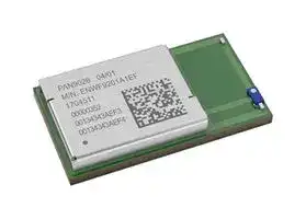


ENWF9202A1EF
Communication Module, WLAN, 5 GHz, SDIO/HS UART/PCM, PAN9026 Series
- Manufacturer: PANASONIC
- Product type:
- SVHC: No SVHC (25-Jun-2025)
- Frequency RF: 5GHz
- Product Range: PAN9026 Series
- Module Interface: SDIO, HS UART, PCM
- Module Applications: Beacons, Industrial IoT, Medical Devices, Smart Home/Building
| Delivery and price | |
|---|---|
| Units per pack | 250 |
| Price | 12.82 € |
| Current stock | 1000+ |
| Lead time | 30 days |
## PAN9026 Wi-Fi Dual Band 2.4/5 GHz and Bluetooth Module Product Specification Rev. 1.1 PAN9026 Wi-Fi/BT Module ## ## **Overview** The PAN9026 is a 2.4/5 GHz ISM band Wi-Fi and Bluetooth radio module, which includes a wireless radio for easy integration of Wi-Fi and Bluetooth connectivity into various electronic devices. - [• ][Power management with sleep clock ] - [Coexistence interface for arbitration of co-] located WLAN, Bluetooth, or Mobile Wireless System (e.g. LTE) - [Generic interfaces include SDIO 3.0 and high-] speed UART for host processor connection - [Software Linux driver ] ## **Features** - [Dual band 2.4/5 GHz 802.11 a/b/g/n Wi-Fi/BT ] combo module - [Supports 802.11i security standards through ] AES, CCMP, and more security mechanisms - [802.11e Quality of Service is supported for ] multimedia applications - [IEEE 802.11n-compliant, 1x1 spatial stream with ] data rates up to MCS7 150 Mbps - [Bluetooth 5.0 (includes LE) ] - [Dual simultaneous and independent WLAN and ] Bluetooth operation - [Dynamic Rapid Channel Switching (DRCS) for ] simultaneous operation in 2.4 GHz and 5 GHz bands - [Indoor location and navigation with ] IEEE 802.11mc ## **Characteristics** - [Surface Mount Type (SMT) ] 17.5 mm x 10.0 mm x 2.6 mm - [Marvell® 88W8977 WLAN 2.4/5 GHz and ] Bluetooth single-chip solution inside - [TX Power +16 dBm @ 802.11b ] - [RX Sensitivity -98 dBm @ 802.11b DSSS ] 1 Mbps - [IEEE 802.11n 20 MHz and 40 MHz ] channel bandwidth - [Long and Short Guard Interval support ] - [Power supply 3.3 V, 2.2 V, 1.8 V ] - [Current consumption Wi-Fi typical 400 mA @ TX ] and 70 mA @ RX - [SDIO 1-bit or 4-bit ] - [Wide temperature range of -30 to +85 °C ] ## **Block Diagram** **==> picture [374 x 253] intentionally omitted <==** **----- Start of picture text -----**<br> VIO 1.8 V<br>PAN9026<br>VDD 2.2 V<br>Crystal Crystal Wi-Fi & Bluetooth Radio Module<br>VDD 1.8 V<br>26 MHz 32.768 kHz IEEE 802.11 a/b/g/n<br>Bluetooth 5.0 (BR, LE & EDR)<br>32 kHz DISABLE<br>GPIOs<br>BPF<br>PDN<br>Chip<br>JTAG Antenna<br>88W8977<br>UART SPDT DPX<br>Radio SoC<br>COEX<br>VIO SD<br>SDIO Interface<br>PCM Interface SPDT<br>CNTL VIO RF 3.3 V RF SW RF Pad<br>50 Ohm<br>**----- End of picture text -----**<br> Product Specification Rev. 1.1 Page 2 PAN9026 Wi-Fi/BT Module By purchase of any of the products described in this document the customer accepts the document's validity and declares their agreement and understanding of its contents and recommendations. Panasonic reserves the right to make changes as required at any time without notification. Please consult the most recently issued Product Specification before initiating or completing a design. © Panasonic Industrial Devices Europe GmbH 2017. This specification sheet is copyrighted. Reproduction of this document is permissible only if reproduction is without alteration and is accompanied by all associated warranties, conditions, limitations, and notices. Do not disclose it to a third party. All rights reserved. This Product Description does not lodge the claim to be complete and free of mistakes. ## **Engineering Samples (ES)** If Engineering Samples are delivered to the customer, these samples have the status “Engineering Samples”. This means that the design of this product is not yet concluded. Engineering Samples may be partially or fully functional, and they may differ from the published Product Specification. Engineering Samples are not qualified and they are not to be used for reliability testing or series production. ## **Disclaimer** The customer acknowledges that samples may deviate from the Product Specification and may bear defects due to their status of development and the lack of qualification mentioned above. Panasonic rejects any liability or product warranty for Engineering Samples. In particular, Panasonic disclaims liability for damages caused by: - The use of the Engineering Sample other than for evaluation purposes, particularly the installation or integration in another product to be sold by the customer, - Deviation or lapse in function of the Engineering Sample, - Improper use of the Engineering Sample. Panasonic Industrial Devices Europe GmbH disclaims any liability for consequential and incidental damages. In case of any queries regarding the Engineering Samples, please contact your local sales partner or the related product manager. Product Specification Rev. 1.1 Page 3 PAN9026 Wi-Fi/BT Module ## ## **Table of Contents** |**1**|**About**|**This Document ......................................................................................................................... 5**| |---|---|---| ||1.1|Purpose and Audience .............................................................................................................. 5| ||1.2|Revision History ......................................................................................................................... 5| ||1.3|Use of Symbols ......................................................................................................................... 5| ||1.4|Related Documents ................................................................................................................... 5| |**2**|**Overview .............................................................................................................................................. 6**|| ||2.1|Block Diagram ........................................................................................................................... 7| ||2.2|Pin Configuration ....................................................................................................................... 8| ||2.3|Power Management................................................................................................................. 12| ||2.4|Host Interfaces ........................................................................................................................ 13| ||2.5|Peripheral Bus Interface .......................................................................................................... 14| ||2.6|PCM Interface .......................................................................................................................... 15| ||2.7|Coexistence ............................................................................................................................. 16| ||2.8|WLAN ...................................................................................................................................... 29| ||2.9|Bluetooth ................................................................................................................................. 34| |**3**|**Detailed Description ......................................................................................................................... 36**|| ||3.1|Dimensions .............................................................................................................................. 36| ||3.2|Footprint .................................................................................................................................. 37| ||3.3|Packaging ................................................................................................................................ 38| ||3.4|Case Marking .......................................................................................................................... 41| |**4**|**Specification ..................................................................................................................................... 42**|| ||4.1|Default Test Conditions ........................................................................................................... 42| ||4.2|Absolute Maximum Ratings ..................................................................................................... 43| ||4.3|Recommended Operating Conditions ...................................................................................... 44| ||4.4|RF Electrical Characteristics .................................................................................................... 63| ||4.5|Reliability Tests ....................................................................................................................... 73| ||4.6|Recommended Soldering Profile ............................................................................................. 74| |**5**|**Cautions ............................................................................................................................................ 75**|| ||5.1|Design Notes ........................................................................................................................... 75| ||5.2|Installation Notes ..................................................................................................................... 75| ||5.3|Usage Condition Notes ............................................................................................................ 76| ||5.4|Storage Notes .......................................................................................................................... 76| ||5.5|Safety Cautions ....................................................................................................................... 76| ||5.6|Other Cautions ........................................................................................................................ 77| ||5.7|Restricted Use ......................................................................................................................... 77| |**6**|**Regulatory and Certification Information ....................................................................................... 79**|| ||6.1|RoHS And REACH Declaration ............................................................................................... 79| |**7**|**Appendix ........................................................................................................................................... 80**|| ||7.1|Ordering Information ................................................................................................................ 80| ||7.2|Acronyms and Abbreviations ................................................................................................... 81| ||7.3|Contact Details ........................................................................................................................ 83| Product Specification Rev. 1.1 Page 4 PAN9026 Wi-Fi/BT Module 1 About This Document ## **1 About This Document** ## **1.1 Purpose and Audience** This Product Specification provides details on the functional, operational, and electrical characteristics of the Panasonic PAN9026 modules. It is intended for hardware design, application, and Original Equipment Manufacturers (OEM) engineers. The product is referred to as “the PAN9026” or “the module” within this document. ## **1.2 Revision History** |**Revision**|**Date**|**Modifications/Remarks**| |---|---|---| |0.1|13.04.2017|First preliminary version| |1.0|20.12.2017|Change to Bluetooth 5.0: Features,2.1 Block Diagram, 2.9 Bluetooth,<br>7.1 Ordering Information<br>Change PM:2.3.1 Power Configuration Example with 3.3 V Host Operation<br>Include values: 4.3.2 Current Consumption, 4.4.3.2 Transmitter Section RF<br>Characteristics<br>Remove section:4.3.7.2 TDM Interface<br>Additional models: 7.1 Ordering Information<br>Add section:7.2 Acronyms and Abbreviations| |1.1|03.07.2018|Rename section: 5.7 Restricted Use<br>Move section: 5.7.1 Life Support Policy<br>Add section:5.7.2 Restricted End Use<br>Additional models:7.1 OrderingInformation| ## **1.3 Use of Symbols** |**Symbol**|**Description**| |---|---| |@|**Note**<br>Indicates important information for the proper use of the product.<br>Non-observance can lead to errors.| |A|**Attention**<br>Indicates important notes that, if not observed, can put the product’s functionality<br>at risk.| |[chapter number]<br>[chapter title]|**Cross reference**<br>Indicates cross references within the document.<br>**Example:**<br>Description of the symbols used in this document1.3 Use of Symbols.| ## **1.4 Related Documents** Please refer to the Panasonic website for related documents 7.3.2 Product Information. Product Specification Rev. 1.1 Page 5 PAN9026 Wi-Fi/BT Module 2 Overview ## **2 Overview** The PAN9026 is a dual band 2.4/5 GHz 802.11 a/b/g/n Wi-Fi radio module with integrated Bluetooth BR/EDR/LE, specifically designed for highly integrated and cost-effective applications. The simultaneous and independent operation of the two standards enables high data rates (802.11n) and low-power operation (Bluetooth Low Energy). Integrated power management, a fast dual-core CPU, 802.11i security standard support, and high-speed data interfaces deliver the performance for the speed, reliability, and quality requirements of next generation products. TX power calibration data and Wi-Fi/Bluetooth system parameters are prestored on the one-time-programmable memory of the PAN9026 during production at Panasonic. This simplifies passing the certification process for PAN9026 customers. Furthermore, the module reduces design, test, and calibration effort resulting in reduced time-to-market compared to discrete solutions. Integrating Wi-Fi and Bluetooth wireless connectivity allows applications such as Smart Energy and home gateways to manage multiple devices and appliances. The combination of Wi-Fi and Bluetooth provides the highest flexibility for connectivity. Please refer to the Panasonic website for related documents 7.3.2 Product Information. Further information on the variants and versions 7.1 Ordering Information. Product Specification Rev. 1.1 Page 6 PAN9026 Wi-Fi/BT Module 2 Overview ## **2.1 Block Diagram** **==> picture [417 x 282] intentionally omitted <==** **----- Start of picture text -----**<br> VIO 1.8 V<br>PAN9026<br>VDD 2.2 V<br>Wi-Fi & Bluetooth Radio Module<br>Crystal Crystal<br>VDD 1.8 V<br>26 MHz 32.768 kHz IEEE 802.11 a/b/g/n<br>Bluetooth 5.0 (BR, LE & EDR)<br>32 kHz DISABLE<br>GPIOs<br>BPF<br>PDN<br>Chip<br>JTAG Antenna<br>88W8977<br>UART SPDT DPX<br>Radio SoC<br>COEX<br>VIO SD<br>SDIO Interface<br>PCM Interface SPDT<br>CNTL VIO RF 3.3 V RF SW RF Pad<br>50 Ohm<br>**----- End of picture text -----**<br> Product Specification Rev. 1.1 Page 7 PAN9026 Wi-Fi/BT Module 2 Overview ## **2.2 Pin Configuration** ## **Pin Assignment** ## Top View **==> picture [322 x 194] intentionally omitted <==** **----- Start of picture text -----**<br> G1 G2 G3 G4 G5 G6 G7 G8 G9<br>©8888 08888<br>F1 F2 F3 F4 F5 F6 F7 F8 F9<br>eeeeeeeee<br>E1 E2 E3 E4 E9<br>@eee 7 e<br>Ground plane<br>D1 D2 D3 D4 EP1 EP2 D9 keep out area<br>C1 C2 C3 C4 C9<br>ooo eeee fal ill ce<br>B1 B2 B3 B4 B5 B6 B7 B8 B9<br>SCCCCOCHC® 7<br>A1 A2 A3 A4 A5 A6 A7 A8 A9<br>ERE<br>17,50 mm<br>(_$$<br>10,00 mm<br>Chip Antenna<br>**----- End of picture text -----**<br> ## **Pin Functions** |**No**|**Pin Name**|**Pin Type**|**Description**| |---|---|---|---| |A11|PCM_DOUT|Output signal|PCM data output signal| ||IO5|Digital I/O|General Purpose IO – GPIO[5]| |A2|32KHZ_IN|NC|Do not connect| |A3|PDN|Input signal|Power down, active-low| |A4|VDD1V8|Power|1.7 V-1.9 V (typ. 1.8 V) power supply connection| |A5|VDD1V8|Power|1.7 V-1.9 V (typ. 1.8 V) power supply connection| |A6|VDD2V2|Power|2.1 V- 2.3 V (typ. 2.2 V) power supply connection| |A7|RF_SW1|Input signal|RF Switch Pin 1 – logical voltage level to activate on-board antenna<br>or RF Pad RF-Switch Pins Function| |A8|GND|Ground pin|Connect to ground| |A9|RF_OUT|RF port|50bottom pad to be activated by RF_SW1/RF_SW2 control<br>voltage RF-Switch Pins Function| |B11|PCM_CLK|Input/output|PCM clock signal, output if PCM master, input if PCM slave| ||IO6|Digital I/O|General Purpose IO – GPIO[6]| 1 Multi-purpose pins: After the firmware download, the pins (GPIO, Serial Interface, RF control) are programmed in functional mode with dedicated functionality. Product Specification Rev. 1.1 Page 8 PAN9026 Wi-Fi/BT Module 2 Overview |**No**|**Pin Name**|**Pin Type**|**Description**| |---|---|---|---| ||||| |B21|PCM_DIN|Input signal|PCM data input signal| ||IO4|Digital I/O|General Purpose IO – GPIO[4]| |B31|PCM_SYNC2|Input/output|PCM Sync Pulse signal, output if PCM master, input if PCM slave| ||IO73|Digital I/O|General Purpose IO – GPIO[7]| |B4|32KHZ_EN|Input Signal|If using VIO 3.3V disable the internal 32.768 kHz crystal oscillator<br>(100to GND) to use the SoC reference clock with lower accuracy| |B5|VDD2V2|Power|2.1 V-2.3 V (typ. 2.2 V) power supply connection| |B6|VDD2V2|Power|2.1 V-2.3 V (typ. 2.2 V) power supply connection| |B7|RF_SW2|Input signal|RF Switch Pin 2 – logical voltage level to activate on-board antenna<br>or RF Pad RF-Switch Pins Function| |B8|GND|Ground pin|Connect to ground| |B9|GND|Ground pin|Connect to ground| |C1|IO2|Digital I/O|General Purpose IO – GPIO[2]| ||DVSC[0]|Output signal|Digital voltage scaling control for PMIC (VOUT 2.2V)<br>Power Configuration Example with 3.3 V HostOperation| |C2|IO3|Digital I/O|General Purpose IO – GPIO[3]| ||DVSC[1]|Output signal|Digital voltage scaling control for PMIC (VOUT 1.05V) - not used| |C3|IO1|Digital I/O|General Purpose IO – GPIO[1]| |C4|COEX_SIN|Input signal|Serial data input from MWS modem or peripheral device| |C9|GND|Ground pin|Connect to ground| |D1|IO15|Digital I/O|General Purpose IO – GPIO[15]| |D2|IO14|Digital I/O|General Purpose IO – GPIO[14]| |D3|DNC_E3|NC|Do not connect| |D4|COEX_SOUT|Output signal|Serial data output to MWS modem or peripheral device| |D9|GND|Ground pin|Connect to ground| |E1|SD_CLK|Digital I/O|For SDIO specific terminals SDIO Pins Function| |E2|SD_CMD|Digital I/O|For SDIO specific terminals SDIO Pins Function| |E3|IO0|Digital I/O|General Purpose IO – GPIO[0]| |E4|DNC_E4|NC|Do not connect| |E9|GND|Ground pin|Connect to ground| |F1|SD_DAT0|Digital I/O|For SDIO specific terminals SDIO Pins Function| 2 PCM Mode: After enabling the mode by host command, the pin is used as PCM Audio Interface. - 3 GPIO Mode: After enabling the mode by host command, the pin is used as Multi-Purpose Interface. Product Specification Rev. 1.1 Page 9 PAN9026 Wi-Fi/BT Module 2 Overview ## |**No**|**Pin Name**|**Pin Type**|**Description**| |---|---|---|---| ||||| |F2|SD_DAT1|Digital I/O|For SDIO specific terminals SDIO Pins Function| |F31|UART_SOUT4|Output Signal|Serial data output to peripheral device| ||IO83|Digital I/O|General Purpose IO – GPIO[8]| ||BT_FREQ5|Input Signal|Information BT using channel which overlaps WLAN channel or not| |F41|UART_SIN4|Input signal|Serial data input to peripheral device| ||IO93|Digital I/O|General Purpose IO – GPIO[9]| ||BT_STATE5|Input signal|Information BT_REQ priority (1- or 2-bit) and direction BT RX/TX| |F51|UART_RTS4|Output signal|Request-to-Send output to peripheral device| ||IO113|Digital I/O|General Purpose IO – GPIO[11]| ||BT_REQ5|Input signal|BT device request access to medium| |F6|IO12|Digital I/O|General Purpose IO – GPIO[12]| |F7|CNTL1|Output signal|Do not connect| |F8|CNTL0|Input signal|Keep open (DNC) if using SDIO interface for BT or connect with<br>100 kto GND if using UART interface for BTControl Pin<br>Function| |F9|GND|Ground pin|Connect to ground| |G1|SD_DAT2|Digital I/O|For SDIO specific terminals SDIO Pins Function| |G2|SD_DAT3|Digital I/O|For SDIO specific terminals SDIO Pins Function| |G3|VIOSD|Power|1.8 V or 3.3 V Digital I/O SDIO power supply| |G4|VIO|Power|1.8 V or 3.3 V power supply for General Purpose IO, if using VIO<br>3.3V disable the internal 32.768 kHz crystal oscillator (Pin No B4)| |G51|UART_CTS4|Input signal|Clear-to-send input from peripheral device| ||IO103|Digital I/O|General Purpose IO – GPIO[10]| ||BT_GRANT5|Output signal|Indicate permission to transmit, low BT can transmit| |G6|IO13|Digital I/O|General Purpose IO – GPIO[13]| |G7|VIORF|Power|3.0 V – 3.6 V (typ. 3.3 V) power supply connection| |G8|DNC|NC|Do not connect| |G9|GND|Ground pin|Connect to ground| |EP1|EPAD1|Thermal pin|Connect to ground| |EP2|EPAD2|Thermal pin|Connect to gorund| 4 UART mode: After the dedicated firmware download, the pin is used as Host Controller Interface (HCI) for Bluetooth. 5 Bluetooth External Coexistence Mode: After enabling the mode by host command, the pin is used as Bluetooth external Coexistence Interface. Product Specification Rev. 1.1 Page 10 PAN9026 Wi-Fi/BT Module 2 Overview ## **SDIO Pins Function** |**No**|**Pin Name**|**Pin Type**|**Description**|**Description**| |---|---|---|---|---| ||||**4-Bit Mode**|**1-Bit Mode**| |E1|SD_CLK|Digital I/O|Clock|Clock| |E2|SD_CMD|Digital I/O|Command Line|Command Line| |F1|SD_DAT0|Digital I/O|Data Line bit [0]|Data Line| |F2|SD_DAT1|Digital I/O|Data Line bit [1] or Interrupt<br>(optional)|Interrupt| |G1|SD_DAT2|Digital I/O|Data Line bit [2] or Read Wait<br>(optional)|Read Wait (optional)| |G2|SD_DAT3|Digital I/O|Data Line bit [3]|Not used| **RF-Switch Pins Function** |**No**<br>**Pin Name**<br>**Pin Type**<br>**Logical Level for Activation**<br>**On-Board Chip Antenna**<br>**RF OUT Pin**<br>A7<br>RF_SW1<br>Input signal<br>3.0 V-3.6 V (typ. 3.3 V)<br>GND (0 V)<br>B7<br>RF_SW2<br>Input signal<br>GND (0 V)<br>3.0 V-3.6 V (typ. 3.3 V)<br>~~————~~|**No**<br>**Pin Name**<br>**Pin Type**<br>**Logical Level for Activation**<br>**On-Board Chip Antenna**<br>**RF OUT Pin**<br>A7<br>RF_SW1<br>Input signal<br>3.0 V-3.6 V (typ. 3.3 V)<br>GND (0 V)<br>B7<br>RF_SW2<br>Input signal<br>GND (0 V)<br>3.0 V-3.6 V (typ. 3.3 V)<br>~~————~~|**No**<br>**Pin Name**<br>**Pin Type**<br>**Logical Level for Activation**<br>**On-Board Chip Antenna**<br>**RF OUT Pin**<br>A7<br>RF_SW1<br>Input signal<br>3.0 V-3.6 V (typ. 3.3 V)<br>GND (0 V)<br>B7<br>RF_SW2<br>Input signal<br>GND (0 V)<br>3.0 V-3.6 V (typ. 3.3 V)<br>~~————~~| |---|---|---| |**Control Pin Function**||| |The control pin is used as configuration input to set parameters following a reset. The definition|The control pin is used as configuration input to set parameters following a reset. The definition|| |of the pin changes immediately after a reset to its usual function. To set a configuration bit to 0,||| |attach a 100 kresistor from the pin to ground. No external circuitry is required to set a||| |configuration bit to 1.||| |**No**|**Pin**<br>**Name**|**Pin Type**|**Strap**<br>**Value**|**WLAN**|**BT/BLE**|**Firmware Download**|**Firmware Download**|**Number SDIO**<br>**Functions**| |---|---|---|---|---|---|---|---|---| |||||||**Type**|**Mode**|| |F8|CNTL0|Input Signal|0|SDIO|UART|SDIO+UART|Parallel/Serial 1 (WLAN)|Parallel/Serial 1 (WLAN)| ||||1|SDIO|SDIO|SDIO+SDIO|Parallel/Serial 2 (WLAN, BT)|Parallel/Serial 2 (WLAN, BT)| The configuration of the control pin is used for the firmware boot option. The software reads and boots accordingly. Product Specification Rev. 1.1 Page 11 PAN9026 Wi-Fi/BT Module 2 Overview ## **2.3 Power Management** ## **2.3.1 Power Configuration Example with 3.3 V Host Operation** **==> picture [410 x 177] intentionally omitted <==** **----- Start of picture text -----**<br> PAN9026<br>VDD 3.3 V 3.3 V<br>VIO RF<br>3.3 V<br>VIO SD<br>PMIC 2.2 V<br>VDD 2.2 V<br>VIN<br>1.8 V<br>VDD 1.8 V<br>1.8 V<br>VDD 3.3 V VIO<br>Enable<br>or Host GPIO<br>3.3 V<br>DVSC[0]<br>88PG823<br>**----- End of picture text -----**<br> ## **2.3.2 Power Configuration Example with 1.8 V Host Operation** **==> picture [413 x 179] intentionally omitted <==** **----- Start of picture text -----**<br> PAN9026<br>VDD 1.8 V 1.8 V<br>VIO/VIO SD<br>DC<br>1.8 V 3.3 V 3.3 V<br>VIO RF<br>DC<br>Step-up 3.3 V DC 2.2 V 2.2 V<br>VDD 2.2 V<br>DC<br>Dual Step-down<br>2.2 V 1.8 V<br>LDO VDD 1.8 V<br>**----- End of picture text -----**<br> Further information 4.3.4 Power-up Sequence. Product Specification Rev. 1.1 Page 12 PAN9026 Wi-Fi/BT Module 2 Overview ## **2.4 Host Interfaces** The bus interface connects several host interface bus units to the CPU bus of the device through the internal bus. The connection of each unit is multiplexed with other bus units. The high-speed UART interface is connected to the CPU bus through a separate bus. |**Type**|**Features**| |---|---| ||| |High-speed UART interface|The device supports a high-speed Universal Asynchronous<br>Receiver/Transmitter (UART) interface, compliant with the industry<br>standard 16550 specification.<br>•FIFO mode permanently selected for transmit and receive operations<br>•Two pins for transmit and receive operations<br>•Two flow control pins<br>•Interrupt triggers for low-power, high throughput operation| |SDIO interface|The device supports an SDIO device interface that conforms to the<br>industry standard SDIO full-speed card specification and allows a host<br>controller using the SDIO bus protocol to access the device.<br>•Supports SDIO 3.0 Standard<br>•1-bit SDIO or 4-bit SDIO transfer modes with full clock range up to<br>100 MHz<br>•On-chip memory used for CIS<br>•Special interrupt register for information exchange<br>•Allows card to interrupt host| Further information 4.3.5 Host Interface Product Specification Rev. 1.1 Page 13 PAN9026 Wi-Fi/BT Module 2 Overview ## **2.5 Peripheral Bus Interface** The Peripheral Bus Unit (PBU) connects several low speed peripherals to the internal bus of the device. The device consists of the GPIO Interface and the One Time Programmable Memory. |**Type**|**Features**| |---|---| ||| |General Purpose I/O<br>(GPIO) Interface|•User-defined GPIOs (each configured to either input or output)<br>•Each GPIO controlled independently<br>•Each I/O configurable to output bit from GPIO_OUT| |One Time Programmable<br>Memory (OTP)|•Storing device-specific calibration data and hardware information like<br>MAC/BD address, WLAN, and Bluetooth parameter<br>•Programmed during production process of device<br>•Device performs calibration when it is powered up| Further information 4.3.6 Peripheral Interface Product Specification Rev. 1.1 Page 14 PAN9026 Wi-Fi/BT Module 2 Overview ## **2.6 PCM Interface** The device supports the PCM interface. |**Type**|**Features**| |---|---| ||| |PCM Interface|•Master or slave mode<br>•PCM bit width size of 8 bits or 16 bits<br>•Up to four slots with configurable bit width and start positions<br>•Short frame and long frame synchronization| Further information 4.3.7 Audio Interface Product Specification Rev. 1.1 Page 15 PAN9026 Wi-Fi/BT Module 2 Overview ## **2.7 Coexistence** The implemented coexistence framework is based on the IEEE 802.15.2 recommended practice Packet Traffic Arbitration (PTA) scheme and the Bluetooth Special Interest Group (BTSIG) Core Specification Volume 7 (Wireless Coexistence Volume). ## **2.7.1 WLAN/Bluetooth Channel Information Exchange** Since Bluetooth and IEEE 802.11 b/g/n WLAN use the same 2.4 GHz frequency band, each can cause interference with another. The level of interference depends on the respective frequency channel used by Bluetooth and WLAN (other factors can impact interference, like Tx power and Rx sensitivity of the device). In a system with both Bluetooth and WLAN, the common host receives information about WLAN channel usage and passes the information to the Bluetooth device. For Bluetooth 1.2 devices with Adaptive Frequency Hopping (AFH) enabled, the Bluetooth device can block channel usage that overlaps the WLAN channel in use. When the Bluetooth device avoids all channels used by the WLAN, the impact of interference is reduced, but not completely eliminated. For Bluetooth 1.1 devices, the Bluetooth device cannot block WLAN channel usage. In this case, a Bluetooth Coexistence Arbiter (BCA) scheme at MAC level is required. The BCA scheme can also be used with Bluetooth 1.2 devices to further reduce the impact of interference to a minimum. ## **2.7.2 External Mobile Wireless System (LTE/ZigBee) and BCA Exchange** Based on the BTSIG Wireless Coexistence Volume, the device supports a Wireless Coexistence Interface 2 (WCI-2) protocol for WLAN/Bluetooth coexistence with an external Mobile Wireless System (MWS), such as a Long Term Evolution (LTE) or ZigBee device. WCI-2 is a 2-wire transport interface. An internal coexistence is used to exchange request/grant with the BCA. Product Specification Rev. 1.1 Page 16 PAN9026 Wi-Fi/BT Module 2 Overview ## **2.7.3 System Configuration** ## **External MWS Device** **==> picture [415 x 280] intentionally omitted <==** **----- Start of picture text -----**<br> RF Front End<br>BCA BT<br>CTL<br>Bluetooth<br>BCA WLAN<br>WLAN CTL<br>BCA<br>MAC<br>MWS to BCA COEX SIN<br>External LTE<br>Device<br>BCA to MWS COEX SOUT<br>88W8977 Radio SoC<br>Host<br>**----- End of picture text -----**<br> ## **External BCA Device** **==> picture [410 x 178] intentionally omitted <==** **----- Start of picture text -----**<br> BT REQ<br>BT STATE BCA WLAN CTL WLAN<br>BCA<br>MAC<br>BT FREQ<br>BT GRANTn<br>88W8977 Radio SoC External BCA Device<br>**----- End of picture text -----**<br> Product Specification Rev. 1.1 Page 17 PAN9026 Wi-Fi/BT Module 2 Overview ## **2.7.4 WCI-2 Interface** The coexistence interface includes a Mobile Wireless System (MWS) transport controller to accommodate a 2-wire, UART-based serial transport interface. This interface is a standard fullduplex UART (TXD and RXD) carrying logical signals framed as UART characters. In addition, it allows support of multiple logical channels. ## **Interface Signals** |**Pin No**|**Signal Name**|**Specification**<br>**Name**|**Pin Type**|**Description**| |---|---|---|---|---| |C4|COEX_SIN|RXD|Input|Serial data from external MWS device| |D4|COEX_SOUT|TXD|Output|Serial data to external MWS device| ## **Signal Waveform Format** The messaging is based on a standard UART format. The UART signals should be connected like a null-modem. For example, the local TXD connected to the remote RXD and vice versa. ## **Interface Transport Settings** |**Item**|**Range**|**Comment**| |---|---|---| |Baudrate|921 600 ~ 4 000 000|Baud| |Data Bits|8|LSB first| |Parity Bits|0|No parity| |Stop Bit|1|One stop bit| |Flow Control|No|No flow control| ## **Supported Baud Rates** |**Baud**|**Baud**|**Baud**|**Baud**| |---|---|---|---| |921 600|2 000 000|3 000 000|4 000 000| Product Specification Rev. 1.1 Page 18 PAN9026 Wi-Fi/BT Module 2 Overview ## **Real-Time Signaling Message** The real-time signaling message is used to transport real-time signals over the 2-wire transport interface. The real-time signaling message conveys the real-time signals (Bluetooth Core Specification, Volume 7, Part A) in one message. The time reference point for the real-time signaling message is the end of message bit 5 (transition to stop bit). Defined real-time signaling messages include: - Coexistence Controller to MWS device - MWS device to Coexistence Controller |**Real-Time Signaling**|**MSG[0]**|**MSG[1]**|**MSG[2]**|**MSG[3]**|**MSG[4]**| |---|---|---|---|---|---| |MWS to Coexistence<br>Controller (Signal)|FRAME_SYNC|MWS_RX|MWS_TX|PATTERN[0]|PATTERN[1]| |Coexistence Controller to<br>MWS (Message)|BT_RX_PRI|BT_TX_ON|802_RX_PRI|802_TX_ON|RFU| ## **Signal Name** FRAME_SYNC MWS_RX MWS_TX PATTERN[1,0] BT_RX_PRI BT_TX_ON 802_RX_PRI 802_TX_ON MWS_INACTIVITY_DURATION MWS_SCAN_FREQUENCY_OFFSET Product Specification Rev. 1.1 Page 19 PAN9026 Wi-Fi/BT Module 2 Overview ## **Transport Control Message** The transport control messages can modify the state and request state information of the MWS coexistence interface. |**Message**|**MSG[0]**|**MSG[1]**|**MSG[2]**|**MSG[3]**|**MSG[4]**| |---|---|---|---|---|---| |Transport Control Message|RESEND_REA<br>L_TIME|RFU|RFU|RFU|RFU| |**Signal Name**|**Description**| |---|---| |RESEND_REAL_TIME|This bit is set if a device wants to get a status update of the real-time signals.<br>The signal is usually used after wake-up from sleep of the transport interface<br>to get an update of the real-time signals.<br>If the receiving device’s transport interface is awake it shall send a real-time<br>message with the current status of the real-time signals within 4 UART<br>character period. If the signal is not transmitted within 4 UART character<br>periods, the device is considered asleep.<br>If the receiving device’s transport interface is not awake it shall not send a<br>real-time message.<br>Bluetooth initiated:<br>If the MWS is currently scanning or has an ongoing inactivity duration, the<br>MWS shall send a frequency scan message or an inactivity duration message<br>after transmitting the real-time message.<br>If the receiving device’s transport interface is not awake it shall not send a<br>frequencyscan or inactivityduration message.| ## **Transparent Data Message** The transport control messages can modify the state and request state information of the MWS coexistence interface. |**Message**|**MSG[0]**|**MSG[1]**|**MSG[2]**|**MSG[3]**|**MSG[4]**| |---|---|---|---|---|---| |Transparent Data Message|NIBBLE_POSI<br>TION|DATA[0]/[4]|DATA[1]/[5]|DATA[2]/[6]|DATA[3]/[7]| ||||||| |**Signal Name**|**Description**||||| |NIBBLE_POSITION|0 = least significant nibble<br>1 = most significant nibble||||| |DATA[n]; n=0 .. 7|Data bits of the message octet||||| Product Specification Rev. 1.1 Page 20 PAN9026 Wi-Fi/BT Module 2 Overview ## **MWS Inactivity Duration Message** The inactivity duration messages is used to send the MWS_INACTIVITY_DURATION signal from the MWS device to the Coexistence Controller. |**Message**|**MSG[0]**|**MSG[1]**|**MSG[2]**|**MSG[3]**|**MSG[4]**| |---|---|---|---|---|---| |MWS Inactivity Duration<br>Message|DURATION[0]|DURATION[1]|DURATION[2]|DURATION[3]|DURATION[4]| The idle duration is encoded in 5 bits given by the formula: Inactivity_Duration = DURATION * 5 ms Inactivity durarations smaller than 5 ms are not communicated. If all bits are set to 1 the inactivity duration is infinite. If all bits are set to 0 or MWS_RX or MWS_TX are set to 1, the inactivity period ends. ## **MWS Scan Frequency Offset Message** The MWS scan frequency offset message is used to send the MWS_SCAN_FREQUENCY_ OFFSET signal from the MWS device to the Coexistence Controller. |**Message**|**MSG[0]**|**MSG[1]**|**MSG[2]**|**MSG[3]**|**MSG[4]**| |---|---|---|---|---|---| |MWS Scan Frequency<br>Offset|BAND|FREQ[0]|FREQ [1]|FREQ [2]|FREQ [3]| The RF scan frequency is encoded in 5 bits given by the formula: RF_FREQ_OFFSET = FREQ * 10 MHz If BAND is set to o the RF_FREQ_OFFSET is the negative value from the lower edge of the ISM band and if BAND is set to 1, RF_FREQ_OFFSET is the positive value from the top edge of the ISM band. FREQ set to all 0 indicates the end of the scan period. Product Specification Rev. 1.1 Page 21 PAN9026 Wi-Fi/BT Module 2 Overview ## **2.7.5 Bluetooth Coexistence Arbiter** |**Type**|**Features**| |---|---| ||| |Capability|•Programmable coexistence interface timing, interface modes, and signal<br>polarity to support a variety of external Bluetooth devices<br>•Programmable decision policies and transaction lock behavior for<br>various use cases<br>•Interface with external or on-chip Bluetooth device<br>•Support Bluetooth 1.1 or Bluetooth 1.2 AFH<br>•WLAN-/Bluetooth-coordinated low-power design<br>•Enhanced information sharing between WLAN and Bluetooth for combo<br>systems<br>•WLAN/Bluetooth/MWS (LTE/ZigBee) coexistence support| |Arbitration|•Contention resolved by a customizable decision matrix that allows<br>independent grant decision for each device<br>•Vectors for the decision matrix:<br>WLAN priority (2-bit)<br>WLAN direction<br>Bluetooth priority (1- or 2-bit)<br>Bluetooth direction<br>Bluetooth frequency in/out band<br>MWS priority (2-bit)<br>MWS direction| |AFH|If AFH is enabled in the Bluetooth device, and there is a sufficient guard-<br>band outside the WLAN operating frequency, the Bluetooth device uses the<br>Out-Of-Band (OOB) channel with respect to the WLAN device. Otherwise,<br>the Bluetooth device uses the In-Band (IB) and OOB channels with respect<br>to the WLAN device.<br>The IB and OOB information is either provided by the Bluetooth device<br>through the coexistence interface, or it can be provided through firmware<br>controls in a shared-host system. IB/OOB is a vector in the decision matrix.| Product Specification Rev. 1.1 Page 22 PAN9026 Wi-Fi/BT Module 2 Overview |**Type**|**Features**| |---|---| ||| |Decision Policies|System configuration is a major consideration when planning decision<br>policies. The configuration governs how RF paths are shared and how<br>much interference will occur. Interference combinations include:<br>WLAN TX and Bluetooth TX<br>WLAN TX and Bluetooth RX<br>WLAN RX and Bluetooth TX<br>WLAN RX and Bluetooth RX<br>Interference combinations where WLAN and Bluetooth share the same<br>antenna:<br>WLAN TX and Bluetooth TX share same antenna, the decision matrix<br>allows either WLAN or Bluetooth TX (both OOB and IB), based on<br>relative packet priorities.<br>WLAN TX and Bluetooth RX (both OOB and IB) have sizable<br>interference impacts on Bluetooth RX, the decision matrix grants or<br>denies WLAN TX based on relative packet priorities.<br>WLAN RX and Bluetooth TX (both OOB and IB) have sizable<br>interference impacts on WLAN RX, the decision matrix grants or<br>denies Bluetooth TX based on relative packet priorities.<br>WLAN RX and Bluetooth RX (both OOB and IB) have no impact on<br>each other, the decision matrix grants both.<br>Interference combinations where WLAN and Bluetooth have their own<br>antenna:<br>WLAN TX and Bluetooth TX in OOB situation have little interference<br>impact on each other, the decision matrix grants both.<br>WLAN TX and Bluetooth TX in IB have sizable interference impact on<br>each other, the decision matrix allows either WLAN or Bluetooth TX,<br>based on relative packet priorities.<br>WLAN TX and Bluetooth RX in OOB situation have little interference<br>impact on each other, the decision matrix grants both provided there<br>is enough antenna isolation between WLAN and Bluetooth antenna.<br>WLAN TX and Bluetooth RX in IB situation have sizable interference<br>impact on Bluetooth RX, the decision matrix grants or denies WLAN<br>TX based on relative packet priorities.<br>WLAN RX and Bluetooth TX in OOB situation have little interference<br>impact on each other, the decision matrix grants both provided there<br>is enough antenna isolation between WLAN and Bluetooth antenna.<br>WLAN RX and Bluetooth TX in IB situation have sizable interference<br>impact on WLAN RX, the decision matrix grants or denies Bluetooth<br>TX based on relative packet priorities.<br>WLAN RX and Bluetooth RX (both OOB and IB) have no impact on<br>each other, the decision matrix grants both.<br>For the devices running in a basic shared antenna configuration, the linear<br>switching imposes restrictions on simultaneous transfer. Reasonable<br>policies include:<br>WLAN and Bluetooth are never granted at the same time<br>Decision matrix grants a device based on relative packet priorities<br>and direction<br>Priority order: High > Medium High > Medium > Low<br>For equal priority contention, select one device to win, that optimizes<br>the usage case<br>For the devices running in an enhanced shared antenna configuration, the<br>linear switching imposes restrictions on some simultaneous transfers.| Product Specification Rev. 1.1 Page 23 PAN9026 Wi-Fi/BT Module 2 Overview |**Type**|**Features**| |---|---| ||| |Transaction Stopping|The arbiter allows control of what transfers can be stopped after an initial<br>grant. If allowed, a transaction can be stopped for higher priority request.<br>A transaction stop decision is a function of the decision policies and<br>transaction stopping control. The transaction stopping control is<br>configurable per device and direction.| Product Specification Rev. 1.1 Page 24 PAN9026 Wi-Fi/BT Module 2 Overview ## **2.7.6 Bluetooth Capability** |**Type**|**Features**| |---|---| ||| |Request Schemes|The PTA signals are directly controlled by the hardware to meet timing<br>requirements of the Bluetooth radio. The software controls the type of traffic<br>in priority mode. Mechanism enforced for control include:<br>•Selection of certain types of communication always treated as high<br>priority<br>•Selection of individual frames marked with high priority<br>•Real-time signaling of the next slot marked with high priority<br>•Automatic hardware control based on the grant/denial history of the<br>Bluetooth link| |Timing Control|The PTA signal timing scheme is fully programmable relative to the<br>Bluetooth packet timing.| Product Specification Rev. 1.1 Page 25 PAN9026 Wi-Fi/BT Module 2 Overview ## **2.7.7 WLAN Capability** |**Type**|**Features**| |---|---| ||| |Capability|The WLAN device technology uses an internal coexistence interface to<br>exchange request/grant with the BCA. Features include:<br>•Packet-based request signaling with direction and priority information<br>•1- or 2-bit priority signaling to support 4 priority levels<br>•Multiple WLAN RX request trigger sources, including early prediction<br>•WLAN TX request cancellation and abort if grant denied or revoked in<br>middle of request<br>•802.11n A-MPDU treated as single packet| |Packet Classification|•Programmable mask allows each frame type to be mapped to a priority<br>•Default setting puts response frames (ACK), beacons, and QoS frames<br>as high priority<br>•WLAN TX and RX have separate priority mask| |Queue Classification|•Programmable mask allows each transmit queue to be mapped to a<br>priority<br>•Queue-based mapping is optional for software-generated frames only| Product Specification Rev. 1.1 Page 26 PAN9026 Wi-Fi/BT Module 2 Overview ## **2.7.8 LTE (MWS) Capability** The device supports a BTSIG WCI-2 MWS coexistence signaling interface. The coexistence logical signaling is designed to enable a standard interface to allow an MWS device and a Coexistence Controller to exchange information and support cooperative coexistence. The WCI-2 signals carry time-critical information such as the start point of an MWS frame. The logical coexistence signaling architecture also includes transparent data messaging and vendor specific data messaging mechanism to enable passing information to and from the collocated MWS device and Coexistence Controller when long latency (tens of milliseconds) cannot be tolerated. Further information 2.7.4 WCI-2 Interface ## **Coexistence Signals** The logical signals assist in time alignment, protecting MWS from interference and maximizing the usability of the Bluetooth radio. ## **Time-Critical Coexistence Signals** |**Signal Name**|**Direction**| |---|---| |FRAME_SYNC|MWS to Bluetooth| |BT_RX_PRI|Bluetooth to MWS| |BT_TX_ON|Bluetooth to MWS| |802_RX_PRI|Bluetooth to MWS| |802_TX_ON|Bluetooth to MWS| |MWS_PATTERN|MWS to Bluetooth| |MWS_RX|MWS to Bluetooth| |MWS_TX|MWS to Bluetooth| |MWS_INACTIVITY_DURATION|MWS to Bluetooth| |MWS_SCAN_FREQUENCY_OFFSET|MWS to Bluetooth| |MWS_TX_PRIL (MWS TX PriorityLevel)|MWS to Bluetooth| |MWS_RX_PRIL (MWS RX Priority Level)|MWS to Bluetooth| Product Specification Rev. 1.1 Page 27 PAN9026 Wi-Fi/BT Module 2 Overview ## **2.7.9 ZigBee (MWS) Coexistence Capability** ZigBee is based on the IEEE 802.15.4 standard and it is used by a suite of communication protocols to create Personal Area Networks (PANs) supporting home automation, lighting control, etc. ZigBee radios operate in the 2.4 GHz ISM band worldwide. Unlike Bluetooth, the ZigBee specification does not use AFH. When coexisting with WLAN/Bluetooth in the 2.4 GHz band, it is important to avoid co-channel (IB) operation of these radios. The device re-uses the MWS coexistence interface to support ZigBee coexistence. The coexistence logical signaling is used to allow a ZigBee device and a WLAN/Bluetooth combo device to exchange information and support cooperative coexistence. ## **Coexistence Signals** The logical signals used for ZigBee and WLAN/Bluetooth coexistence are a subset of the LTE coexistence signaling. Considering the lower data rate of ZigBee packets, a lower baud rate may be chosen for the 2-wire UART physical interface. The BCA supports 3-way arbitration among ZigBee/WLAN/Bluetooth requests. ## **Coexistence Signals** |**Signal Name**|**Direction**| |---|---| |MWS_RX|MWS to Bluetooth| |MWS_TX|MWS to Bluetooth| |MWS_PATTERN|MWS to Bluetooth| |MWS_RX_PRI|MWS to Bluetooth| |MWS_TX_PRI|MWS to Bluetooth| |802_RX_PRI|Bluetooth to MWS| |802_TX_ON|Bluetooth to MWS| |BT_RX_PRI|Bluetooth to MWS| |BT_TX_ON|Bluetooth to MWS| Product Specification Rev. 1.1 Page 28 PAN9026 Wi-Fi/BT Module 2 Overview ## **2.8 WLAN** |**Type**|**Features**| |---|---| ||| |IEEE 802.11/<br>Standards|•802.11 data rates 1 and 2 Mbps (DSSS)<br>•802.11b data rates 5.5 and 11 Mbps (CCK)<br>•802.11a/g data rates 6, 9, 12, 18, 24, 36, 48, and 54 Mbps (OFDM)<br>•802.11b/g performance enhancements<br>•802.11n with maximum data rates up to 72 Mbps (20 MHz channel) and<br>150 Mbps (40 MHz channel)<br>•802.11e quality of service (QoS)<br>•802.11h transmit power control<br>•802.11h DFS radar pulse detection<br>•802.11i enhanced security (WEP, WPA, WPA2)<br>•802.11k radio resource measurement<br>•802.11mc precise indoor location and navigation<br>•802.11n block acknowledgment extension<br>•802.11r fast hand-off for AP roaming<br>•802.11u Hotspot 2.0 (STA mode only)<br>•802.11v TIM frame transmission/reception<br>•802.11w protected management frames<br>•Support clients (stations) implementing IEEE Power Save mode| |WLAN MAC|•Frame exchange at the MAC level to deliver data<br>•Received frame filtering and validation (CRC)<br>•Generation of MAC header and trailer information (MPDUs)<br>•Fragmentation of data frames (MSDUs)<br>•Access mechanism support for fair access to shared wireless medium<br>through:<br>Distributed Coordination Function (DCF)<br>Enhanced Distributed Channel Access (EDCA)<br>•A-MPDU aggregation/de-aggregation<br>•20/40 MHz channel coexistence<br>•RIFS burst receive<br>•Management information base<br>•Radio resource measurement<br>•Quality of service<br>•Block acknowledgement<br>•Dynamic frequency selection<br>•TIM frame TX and RX<br>•Multiple BSS/Station<br>•Transmit rate adaption<br>•Transmit power control| Product Specification Rev. 1.1 Page 29 PAN9026 Wi-Fi/BT Module 2 Overview ## |**Type**|**Features**| |---|---| ||| |WLAN Baseband|•802.11n 1x1 SISO (WLAN SoC with SISO RF radio)<br>•Backward compatibility with legacy 802.11a/b/g technology<br>•WLAN/Bluetooth LNA sharing<br>•PHY data rates up to 150 Mbps<br>•20 MHz bandwidth/channel, 40 MHz bandwidth/channel, upper/lower<br>20 MHz bandwidth in 40 MHz channel, and 20 MHz duplicate legacy<br>bandwidth in 40 MHz channel mode operation<br>•Modulation and Coding Scheme MCS 0 ~ 7 and MCS 32 (duplicate<br>6 Mbps)<br>•Dynamic frequency selection (radar detection)<br>–<br>Enhanced radar detection for short and long pulse radar<br>–<br>Enhanced AGC scheme for DFS channel<br>–<br>Japan DFS requirement for W53 and W56<br>•802.11k Radio resource measurement<br>•802.11n optional features:<br>–<br>20/40 MHz coexistence<br>–<br>Space-Time-Block-Coding (STBC) one spatial stream reception<br>and transmission<br>–<br>Short Guard Interval for both 20 and 40 MHz operation (TX/RX)<br>–<br>RIFS on receive path<br>–<br>Beamformer function and hardware acceleration<br>–<br>Greenfield TX/RX<br>•802.11mc locationing<br>•Power save features| |WLAN Radio|•Integrated direct-conversion radio<br>•20 and 40 MHz channel bandwidth<br>•Shared WLAN/Bluetooth receive input scheme for 2.4 GHz band<br>•RX Path<br>On-chip gain selectable LNA with optimized noise figure and power<br>consumpttion<br>High dynamic range AGC function in receive mode<br>•TX Path<br>Internal PA with power control<br>Optimized TX gain distribution for linearity and noise performance<br>•Local Oscillator with fine channel step| |WLAN Encryption|•WEP 64-bit and 128-bit encryption with hardware TKIP processing<br>(WPA)<br>•AES-CCMP hardware implementation as part of 802.11i security<br>standard (WPA2)<br>•Enhanced AES engine performance<br>•Advanced encryption standard (AES)/Counter-Mode/CBC-MAC Protocol<br>(CCMP)<br>•AES-Cipher-Based Message Authentication Code (CMAC) as part of the<br>802.11w security standard<br>•WLAN Authentication and Privacy Infrastructure (WAPI)| Product Specification Rev. 1.1 Page 30 PAN9026 Wi-Fi/BT Module 2 Overview ## **Operation Modes** |**Parameter**|**Operation Mode**|**Operation Mode**|**Operation Mode**||**Specification**| |---|---|---|---|---|---| |Standard Conformance|IEEE 802.11/IEEE 802.11b||||| ||IEEE 802.11a||||| ||IEEE 802.11g||||| ||IEEE 802.11n||||| |Modulation|IEEE 802.11a||||OFDM| ||IEEE 802.11b||||DSSS/CCK| ||IEEE 802.11g||||OFDM| ||IEEE 802.11n||||OFDM @ MCS0~7 and MCS32 (duplicate<br>6 Mbps)| |Physical layer data rates|IEEE 802.11||||1, 2 Mbps @ DSSS| ||IEEE 802.11b||||5.5, 11 Mbps @ DSSS/CCK| |Supported data rates|IEEE 802.11g||||6, 9, 12, 18, 24, 36, 48, 54 Mbps| ||IEEE 802.11a||||6, 9, 12, 18, 24, 36, 48, 54 Mbps| ||IEEE<br>802.11n|MCS0~7|HT20|LGI|6.5, 13, 19.5, 26, 39, 52, 58.5, 65 Mbps| |||||SGI|7.2, 14.4, 21.7, 28.9, 43.3, 57.8, 65,<br>72.2 Mbps| ||||HT40|LGI|13.5, 27, 40.5, 54, 81, 108, 121.5,<br>135 Mbps| |||||SGI|15, 30, 45, 60, 90, 120, 135, 150 Mbps| |Supported bandwidth|IEEE 802.11n||||20, 40 MHz (BW)| |Supported channel mode<br>operation|IEEE 802.11n||||20 MHz BW/channel, 40 MHz BW/channel,<br>upper/lower 20 MHz BW @ 40 MHz<br>channel, 20 MHz duplicate legacy BW<br>@ 40 MHz channel| |Supported Guard Interval|IEEE 802.11n||||400 ns (SGI), 800 ns (LGI)| Product Specification Rev. 1.1 Page 31 PAN9026 Wi-Fi/BT Module 2 Overview ## **Supported Channels and Frequencies** |**2.4 GHz – IEEE 802.11b/g/n**|**2.4 GHz – IEEE 802.11b/g/n**||||| |---|---|---|---|---|---| |**20 MHz Channels**|||**40 MHz Channels**||| |**Channel**|**Frequency**|**Unit**|**Channel**|**Frequency**|**Unit**| |1|2 412|MHz|1-5|2 422|MHz| |2|2 417|MHz|2-6|2 427|MHz| |3|2 422|MHz|3-7|2 432|MHz| |4|2 427|MHz|4-8|2 437|MHz| |5|2 432|MHz|5-9|2 442|MHz| |6|2 437|MHz|6-10|2 447|MHz| |7|2 442|MHz|7-11|2 452|MHz| |8|2 447|MHz|||| |9|2 452|MHz|||| |10|2 457|MHz|||| |11|2 462|MHz|||| |12|2 467|MHz|||| |13|2 472|MHz|||| |**5 GHz – IEEE 802.11a/n**|**5 GHz – IEEE 802.11a/n**||||| |---|---|---|---|---|---| |**20 MHz Channels**|||**40 MHz Channels**||| |**Channel**|**Frequency**|**Unit**|**Channel**|**Frequency**|**Unit**| |36|5 180|MHz|36-40|5 190|MHz| |40|5 200|MHz|44-48|5 230|MHz| |44|5 220|MHz|52-56|5 270|MHz| |48|5 240|MHz|60-64|5 310|MHz| |52|5 260|MHz|||| |56|5 280|MHz|||| |60|5 300|MHz|||| |64|5 320|MHz|||| ||||||| |100|5 500|MHz|100-104|5 510|MHz| |104|5 520|MHz|108-112|5 550|MHz| |108|5 540|MHz|116-120|5 590|MHz| |112|5 560|MHz|124-128|5 630|MHz| |116|5 580|MHz|132-136|5 670|MHz| |120|5 600|MHz|||| |124|5 620|MHz|||| |128|5 640|MHz|||| |132|5 660|MHz|||| |136|5 680|MHz|||| |140|5 700|MHz|||| Product Specification Rev. 1.1 Page 32 PAN9026 Wi-Fi/BT Module 2 Overview |**5 GHz – IEEE 802.11a/n**|**5 GHz – IEEE 802.11a/n**||||| |---|---|---|---|---|---| |**20 MHz Channels**|||**40 MHz Channels**||| |**Channel**|**Frequency**|**Unit**|**Channel**|**Frequency**|**Unit**| |149|5 745|MHz|149-153|5 755|MHz| |153|5 765|MHz|157-161|5 795|MHz| |157|5 785|MHz|||| |161|5 805|MHz|||| |165|5 825|MHz|||| |**5 GHz – IEEE 802.11a/n (India and additional UNII**|**5 GHz – IEEE 802.11a/n (India and additional UNII**|**5 GHz – IEEE 802.11a/n (India and additional UNII**|**Channels)**|**Channels)**|| |---|---|---|---|---|---| |**20 MHz Channels**|||**40 MHz Channels**||| |**Channel**|**Frequency**|**Unit**|**Channel**|**Frequency**|**Unit**| |144|5 720|MHz|68-72|5 350|MHz| |1696|5 845|MHz|76-80|5 390|MHz| |173|<br>5 865|MHz|84-88|5 430|MHz| |177|5 885|MHz|92-96|5 470|MHz| |181|5 905|MHz|140-144|5 710|MHz| ||||165-169|5 835|MHz| ||||169-1737|5 855|MHz| ||||173-177|5 875|MHz| > 6 India channels that can be used in other countries as well > 7 India use only Product Specification Rev. 1.1 Page 33 PAN9026 Wi-Fi/BT Module 2 Overview ## **2.9 Bluetooth** |**Type**|**Features**| |---|---| ||| |General|•Supports Bluetooth 5.0<br>•Shared Tx/Rx path for Bluetooth<br>•Digital Audio Interface including PCM interface for voice application<br>•Bluetooth and WLAN coexistence<br>•WLAN/Bluetooth Coexistence (BCA) protocol support| |Bluetooth Classic<br>(BR/EDR)|•Bluetooth Classic with BT Class 1 support<br>•Baseband and radio Basic Rate (BR) and Enhanced Data Rate (EDR)<br>packet types with 1 Mbps (GFSK), 2 Mbps (π/4-DQPSK) and 3 Mbps<br>(8DPSK)<br>•Fully functional Bluetooth baseband with:<br>–<br>Adaptive Frequency Hopping (AFH)<br>–<br>Forward error correction<br>–<br>Header error control<br>–<br>Access code correlation<br>–<br>CRC<br>–<br>Encryption bit stream generation<br>–<br>Whitening<br>•Adaptive Frequency Hopping (AFH) including Packet Loss Rate (PLR)<br>•Interlaced scan for faster connection setup<br>•Simultaneous active ACL connection support<br>•Automatic ACL packet type selection<br>•Full master slave piconet support<br>•Scatternet support<br>•Standard UART and SDIO HCI transport layer<br>•SCO/eSCO links with hardware accelerated audio signal pocessing and<br>hardware supported PPEC algorithm for speech quality improvement<br>•All standard SCO/eSCO voice coding<br>•All standard pairing, authentication, link key, and encryption operations<br>•Standard Bluetooth power saving mechanism (i.e. hold, sniff modes, and<br>sniff-sub rating)<br>•Enhanced Power Control (EPC)<br>•Channel Quality Driven (CQD) data rate<br>•Wideband Speech (WBS) support (1 WBS link)<br>•Encryption (AES) support<br>•LTE/MWS coexistence| Product Specification Rev. 1.1 Page 34 PAN9026 Wi-Fi/BT Module 2 Overview |**Type**|**Features**| |---|---| ||| |Bluetooth Low Energy (LE)|•Broadcaster, Observer, Central, and Peripheral roles<br>•Supports link layer topology to be master and slave (connects up to<br>16 links)<br>•Shared RF with BR/EDR<br>•Encryption AES support<br>•Hardware support for intelligent Adaptive Frequency Hopping (AFH)<br>•LE Privacy 1.2<br>•LE Secure Connection<br>•LE Data Length Extension<br>•LE Advertising Length Extension<br>•Direction Finding<br>–<br>Connection-oriented Angle of Arrival (AoA)| Product Specification Rev. 1.1 Page 35 PAN9026 Wi-Fi/BT Module 3 Detailed Description ## **3 Detailed Description** ## **3.1 Dimensions** **==> picture [32 x 31] intentionally omitted <==** **----- Start of picture text -----**<br> @<br>**----- End of picture text -----**<br> All dimensions are in millimeters. **==> picture [170 x 207] intentionally omitted <==** **----- Start of picture text -----**<br> <><br>17,50<br>10<br>2,55<br>**----- End of picture text -----**<br> |**No.**|**Item**|**Dimension**|**Tolerance**|**Remark**| |---|---|---|---|---| |1 Width|1 Width|10.00|± 0.35|± 0.35| |2 Length|2 Length|17.50|± 0.35|± 0.35| |3 Height|3 Height|2.55|± 0.20 with case|± 0.20 with case| Product Specification Rev. 1.1 Page 36 PAN9026 Wi-Fi/BT Module 3 Detailed Description ## **3.2 Footprint** The outer dimensions have a tolerance of 0.35 mm. ## Top View **==> picture [449 x 524] intentionally omitted <==** **----- Start of picture text -----**<br> 8,8 0 mm<br>6,0 0 mm<br>2,20 mm 2,20 mm<br>G1 G2 G3 G4 G5 G6 G7 G8 G9<br>0,80 mm<br>F1 F2 F3 F4 F5 F6 F7 F8 F9<br>E1 E2 E3 E4 E9<br>Ground plane<br>D1 D2 D3 D4 EP1 EP2 D9 keep out area<br>C1 C2 C3 C4 C9<br>B1 B2 B3 B4 B5 B6 B7 B8 B9<br>0,80 mm<br>A1 A2 A3 A4 A5 A6 A7 A8 A9<br>cS |<br>0,80 mm 1,40 mm 4,8 0 mm<br>2,20 mm<br>3,60 mm<br>5,00 mm<br>6,40 mm<br>7,80 mm<br>9,20 mm<br>10,60 mm<br>12,00 mm<br>12,00 mm<br>—<br>17,50 mm<br>Product Specification Rev. 1.1<br>Chip Antenna<br>9,20 mm 7,80 mm 6,80 mm 6,40 mm 5,00 mm 3,60 mm 3,20 mm 2,20 mm 0,80 mm 1.00 mm<br>00 mm,<br>0,80 mm 8.00 mm<br>10<br>1.00 mm<br>**----- End of picture text -----**<br> Page 37 PAN9026 Wi-Fi/BT Module 3 Detailed Description ## ## **3.3 Packaging** The product is a mass production status product and will be delivered in the package described below. ## **3.3.1 Tape Dimensions** **==> picture [400 x 228] intentionally omitted <==** **----- Start of picture text -----**<br> T Do P2 Po E1<br>0.30± 0.03 +0.1 2.0± 0.15(I) 4.0± 0.15(II) 1.75± 0.1<br>1.5 0.0 Y<br>D1<br>= 6 2.0MIN 2 0 G0 00i0/0 0 00 —GG9 00000 4 ; |<br>X X<br>| Bjlooo A oo Y po0do0po000e a<br>Ko P1 Ao<br>SECTION Y-Y R0.75<br>DETAIL A SECTION X-X<br>Ao 10.55 +/- 0.15<br>Bo 18.05 +/- 0.15 (I) Measured from centreline of sprocket hole<br>Ko 3.00 +/- 0.15 to centreline of pocket.<br>F 14.20 +/- 0.15 (II) Cumulative tolerance of 10 sprocketholes is ± 0.20 .<br>P 1 20.00 +/- 0.15 (III) Measured from centreline of sprocket<br>S O 28.40 +/- 0.15 (IV) hole to centreline of pocket.Other material available.<br>W 32.00 +/- 0.3 ALL DIMENSIONS IN MILLIMETRES UNLESS OTHERWISE STATED.<br>F(III)<br>Bo So W<br>± 0.05<br>0.20<br>**----- End of picture text -----**<br> ## **3.3.2 Packing in Tape** Empty spaces in the component packed area shall be less than two per reel and those spaces shall not be consecutive. The top cover tape shall not be found on reel holes and it shall not stick out from the reel. Product Specification Rev. 1.1 Page 38 PAN9026 Wi-Fi/BT Module 3 Detailed Description ## **3.3.3 Component Direction** ## **3.3.4 Reel Dimension** Product Specification Rev. 1.1 Page 39 PAN9026 Wi-Fi/BT Module 3 Detailed Description ## **3.3.5 Package Label** ## **Example** |(1T)|Lot code| |---|---| |(1P)|Customer order number, if applicable| |(2P)|Order number| |(9D)|Date code| |(Q)|Quantity| |(HW/SW)|Hardware/software version| ## **3.3.6 Total Package** **==> picture [374 x 228] intentionally omitted <==** **----- Start of picture text -----**<br> moisture-sensitive print<br>(already exist on barrier bag) barcode<br>label<br>; o o<br>barrier bag<br>sealed<br>desiccant 1) 2)<br>moisture indicator<br>Ca” “S g<br>1) quantity of desiccant according<br> to calculation<br>barcode 2) optional: desiccant placed into<br>label the corner of the barrier bag<br>ON ><br>inner carton box<br>SSZA<br>size 340 x 340 x 41 mm³<br>**----- End of picture text -----**<br> Product Specification Rev. 1.1 Page 40 PAN9026 Wi-Fi/BT Module 3 Detailed Description ## **3.4 Case Marking** ## **Example for PAN9026 (top view)** **==> picture [240 x 194] intentionally omitted <==** **----- Start of picture text -----**<br> 2 3<br>1<br>PAN9026 HW/SW ES<br>4 M/N: ENWF9201A1EF<br>5 YYWWDLL<br>6 12345678<br>7 0013430B801E<br>8 0013430B801F<br>9 11<br>10<br>**----- End of picture text -----**<br> **==> picture [204 x 183] intentionally omitted <==** **----- Start of picture text -----**<br> 1 Brand name<br>2 Hardware/Software version<br>3 Engineering Sample (optional)<br>4 Model Name/ENW number<br>5 Lot code<br>6 Serial number<br>7 WLAN MAC address<br>8 BD address<br>9 (Reserved)<br>10 Marking for Pin 1<br>11 2D barcode, for internal usage only<br>**----- End of picture text -----**<br> Product Specification Rev. 1.1 Page 41 PAN9026 Wi-Fi/BT Module 4 Specification ## **4 Specification** **==> picture [32 x 32] intentionally omitted <==** **----- Start of picture text -----**<br> ®@<br>**----- End of picture text -----**<br> All specifications are over temperature and process, unless indicated otherwise. ## **4.1 Default Test Conditions** ®@ |Temperature:<br>Humidity:<br>Supply Voltage:|Temperature:<br>Humidity:<br>Supply Voltage:|25 ± 10 °C<br>40 to 85 % RH<br>VDD2V2|= 2.2 V| |---|---|---|---| |||VDD1V8|= 1.8 V| |||VIORF|= 3.3 V| |||VIOSD|= 3.3 V| |||VIO|= 1.8 V| Product Specification Rev. 1.1 Page 42 PAN9026 Wi-Fi/BT Module 4 Specification ## **4.2 Absolute Maximum Ratings** The maximum ratings may not be exceeded under any circumstances, not even momentarily or individually, as permanent damage to the module may result. |**Symbol**|**Parameter**|**Condition**|**Min.**|**Typ.**|**Max.**|**Units**| |---|---|---|---|---|---|---| |TSTOR|Storage<br>temperature||-55||+125|°C| |VESD|ESD<br>robustness|All pads, according to human<br>body model (HBM), JEDEC<br>STD 22, method A114|||1 000|V| |||According to charged device<br>model (CDM), JEDEC STD 22,<br>method C101|||500|V| |PRF|RF input level|RF input level|||+20|dBm| |VDD1V8|Maximum<br>voltage|Maximum power supply voltage<br>from any pin with respect to<br>VSS(GND)||1.8|1.98|V| |VDD2V2||||2.2|2.3|V| |VIOSD||||1.8|2.2|V| |||||3.3|4.0|V| |VIO||||1.8|2.2|V| |||||3.3|4.0|V| |VIORF||||3.3|4.0|V| |VRF_SW1/2||||3.3|4.0|V| Product Specification Rev. 1.1 Page 43 PAN9026 Wi-Fi/BT Module 4 Specification ## **4.3 Recommended Operating Conditions** The maximum ratings may not be exceeded under any circumstances, not even momentarily or individually, as permanent damage to the module may result. |**Symbol**|**Parameter**|**Condition**|**Min.**|**Typ.**|**Max.**|**Units**| |---|---|---|---|---|---|---| |TA|Ambient<br>operating<br>temperature<br>range|Extended grade|-30||+85|°C| |VDD1V8|1V8 supply<br>voltage8|VDD voltage on pins A4, A5|1.71|1.80|1.89|V| |VDD2V2|2V2 supply<br>voltage8|VDD voltage on pins A6, B5, B6|2.09|2.20|2.29|V| |VIOSD|Digital I/O<br>VIOSD supply<br>voltage9|Pin G3 with 1.8 V operation<br>SDIO Pins Function|1.62|1.80|1.98|V| |||Pin G3 with 3.3 V operation<br>SDIO Pins Function|2.97|3.30|3.47|V| |VIO|Digital I/O VIO<br>supply voltage|Pin G4 with 1.8 V operation|1.62|1.80|1.98|V| |||Pin G4 with 3.3 V operation<br>Pin B4 connect to GND10|2.97|3.30|3.47|V| |VIORF|Digital I/O<br>VIORF supply<br>voltage8|Pin G7 with 3.3 V operation|2.97|3.30|3.47|V| |VRF_SW1/2|VRF_SW1/2<br>switch<br>voltage8|Pin A7, B7 with 3.3 V logical<br>level switch operation<br>RF-Switch Pins Function||3.30|3.60|V| > 8 The supply current must be limited to max. 1 A > 9 1.8 V or 3.3 V supply voltage possible > 10 Connect the 32KHZ_EN pin via a 100 resistor to ground to disable the internal 32.768 kHz crystal oscillator. The low power modes will then use the SoC reference clock, which has lower accuracy. Product Specification Rev. 1.1 Page 44 PAN9026 Wi-Fi/BT Module 4 Specification ## **4.3.1 Digital Pin Characteristics** ## **VIO with 1.8 V Operations[11]** |**Symbol**|**Parameter**|**Condition**|**Min.**|**Typ.**|**Max.**|**Units**| |---|---|---|---|---|---|---| |VIH|High level input<br>voltage|1.8 V operation (VIO= 1.8 V)|0.7 VIO||VIO+ 0.4|V| |VIL|Low level input<br>voltage|1.8 V operation (VIO= 1.8 V)|-0.4||0.3 VIO|V| |VHYS|Input hysteresis||100|||mV| |VOH|High level ouput<br>voltage|1.8 V operation (VIO= 1.8 V)|VIO- 0.4|||V| |VHO|Low level<br>output voltage|1.8 V operation (VIO= 1.8 V)|||0.4|V| ## **VIO with 3.3 V Operations[11]** |**Symbol**|**Parameter**|**Condition**|**Min.**|**Typ.**|**Max.**|**Units**| |---|---|---|---|---|---|---| |VIH|High level input<br>voltage|3.3 V operation (VIO= 3.3 V)|0.7 VIO||VIO+ 0.4|V| |VIL|Low level input<br>voltage|3.3 V operation (VIO= 3.3 V)|-0.4||0.3 VIO|V| |VHYS|Input hysteresis||100|||mV| |VOH|High level ouput<br>voltage|3.3 V operation (VIO= 3.3 V)|VIO- 0.4|||V| |VHO|Low level<br>output voltage|3.3 V operation (VIO= 3.3 V)|||0.4|V| **VIOSD 1.8 V Operation for SDIO I/F[11]** |**Symbol**|**Parameter**|**Condition**|**Min.**|**Typ.**|**Max.**|**Units**| |---|---|---|---|---|---|---| |VIH|High level input<br>voltage|1.8 V operation (VIOSD= 1.8 V)|0.7 VIOSD||VIOSD<br>+0.4|V| |VIL|Low level input<br>voltage|1.8 V operation (VIOSD= 1.8 V)|-0.4||0.3 VIOSD|V| |VHYS|Input hysteresis||100|||mV| |VOH|High level ouput<br>voltage|1.8 V operation (VIOSD= 1.8 V)|VIOSD<br>- 0.4|||V| |VHO|Low level<br>output voltage|1.8 V operation (VIOSD= 1.8 V)|||0.4|V| > 11 The capacitive load should not be larger than 50 pF for all I/Os when using the default driver strength settings. Large capacitance loads generally increase the overall current consumption. Product Specification Rev. 1.1 Page 45 PAN9026 Wi-Fi/BT Module 4 Specification **VIOSD 3.3 V Operation for SDIO I/F[11]** |**Symbol**|**Parameter**|**Condition**|**Min.**|**Typ.**|**Max.**|**Units**| |---|---|---|---|---|---|---| |VIH|High level input<br>voltage|3.3 V operation (VIOSD= 3.3 V)|0.7 VIO_SD||VIO_SD<br>+0.4|V| |VIL|Low level input<br>voltage|3.3 V operation (VIOSD= 3.3 V)|-0.4||0.3 VIO_SD|V| |VHYS|Input hysteresis|Input hysteresis|100|||mV| |VOH|High level ouput<br>voltage|3.3 V operation (VIOSD= 3.3 V)|VIOSD<br>- 0.4|||V| |VHO|Low level<br>output voltage|3.3 V operation (VIOSD= 3.3 V)|||0.4|V| For SDIO 3.0 standard modes SDR12, SDR25, SDR50, and DDR50, a supply voltage of VIOSD = 1.8 V should be used. Product Specification Rev. 1.1 Page 46 PAN9026 Wi-Fi/BT Module 4 Specification ## **4.3.2 Current Consumption** The current consumption depends on the user scenario, the setup and timing of the power modes. Assume VDD2V2 = 2.2 V, VDD1V8 = 1.8 V, VIORF = 3.3 V, VIOSD = 3.3 V, VIO = 1.8 V, and Tamb = 25 °C, if nothing else stated. ## **General Current Consumption** |**Symbol**|**Parameter**|**Condition**|**Min.**|**Typ.**|**Max.**|**Units**| |---|---|---|---|---|---|---| |IVDD1V8 @ PDn|Power Down|Grounding of PDn pin||150||µA| |IVDD2V2 @ PDn||||5||µA| |IVDD1V8 @ DeepSleep|WLAN / BT<br>Deep Sleep|Low-power state used in sleep state|Low-power state used in sleep state|600||µA| |IVDD2V2 @ DeepSleep||||5||µA| |IVDD1V8 @ Firmware InitFirmware|Firmware<br>Initialization|Device Initialization||400||mA| |IVDD2V2 @ Firmware Init||||950||mA| ## **WLAN Current Consumption** |**Symbol**|**Parameter**|**Condition**|**Min.**|**Typ.**|**Max.**|**Units**| |---|---|---|---|---|---|---| |IVDD1V8 @ TX|Active<br>Transmit12|PTX= +15 dBm for 5 GHz band<br>802.11a @ 54 Mbps||230||mA| |||PTX= +14 dBm for 5 GHz band<br>802.11n 20M @ MCS7||240||mA| |||PTX= +13 dBm for 5 GHz band<br>802.11n 40M @ MCS7||250||mA| |||PTX= +16 dBm for 2.4 GHz band<br>802.11b @ 11 Mbps||175||mA| |||PTX= +15 dBm for 2.4 GHz band<br>802.11g @ 54 Mbps||180||mA| |||PTX= +14 dBm for 2.4 GHz band<br>802.11n 20M @ MCS7||185||mA| |IVDD2V2 @ TX|Active<br>Transmit12|PTX= +15 dBm for 5 GHz band<br>802.11a @ 54 Mbps||180||mA| |||PTX= +14 dBm for 5 GHz band<br>802.11n 20M @ MCS7||170||mA| |||PTX= +13 dBm for 5 GHz band<br>802.11n 40M @ MCS7||160||mA| |||PTX= +16 dBm for 2.4 GHz band<br>802.11b @ 11 Mbps||240||mA| |||PTX= +15 dBm for 2.4 GHz band<br>802.11g @ 54 Mbps||190||mA| |||PTX= +14 dBm for 2.4 GHz band<br>802.11n 20M @ MCS7||170||mA| 12 Peak values for specified output power level and data rate with UDP traffic between the AP and Device (STA). Product Specification Rev. 1.1 Page 47 PAN9026 Wi-Fi/BT Module 4 Specification |**Symbol**|**Parameter**|**Condition**|**Min.**|**Typ.**|**Max.**|**Units**| |---|---|---|---|---|---|---| |IVDD1V8 @ RX|Active<br>Receive13|5 GHz band 802.11a @ 54 Mbps||85||mA| |||5 GHz band 802.11n 20M @ MCS7||95||mA| |||5 GHz band 802.11n 40M @ MCS7||110||mA| |||2.4 GHz band 802.11b @ 11 Mbps||65||mA| |||2.4 GHz band 802.11g @ 54 Mbps||70||mA| |||2.4 GHz band 802.11n 20M<br>@ MCS7||75||mA| |IVDD2V2 @ RX|Active<br>Receive13|5 GHz band 802.11a/n||20||µA| |||2.4 GHz band 802.11b/g/n||20||µA| |IVDD1V8 @ IEEE-PS|IEEE Power<br>Save14|DTIM = 1 with beacon interval<br>100 ms (Average15)||2||mA| |IVDD2V2 @ IEEE-PS||||20||µA| ## **Bluetooth Current Consumption** |**Symbol**|**Parameter**|**Condition**|**Min.**|**Typ.**|**Max.**|**Units**| |---|---|---|---|---|---|---| |IVDD1V8 @ TX|BT SCO HV3|Peak, PTX= +4 dBm||55||mA| ||BT ACL DH1|Average, PTX= 0 dBm||25||mA| ||BT ACL 3-DH5|Average, PTX= 0 dBm||35||mA| ||LE|PTX= 0 dBm||45||mA| |IVDD2V2 @ TX|BT SCO HV3|PTX= +4 dBm||15||µA| ||BT ACL DH1|PTX= 0 dBm||15||µA| ||BT ACL 3-DH5|PTX= 0 dBm||15||µA| ||LE|PTX= 0 dBm||15||µA| |IVDD1V8 @ RX|LE|Peak||30||mA| |IVDD2V2 @ RX|LE|||5||µA| |IVDD1V8 @ Page Scan|BT Page Scan|Peak||2.4||mA| |IVDD2V2 @ Page Scan||||5||µA| |IVDD1V8 @ PI Scan|BT Page and<br>Inquiry Scan|Peak||3.8||mA| |IVDD2V2 @ PI Scan||||5||µA| |IVDD1V8 @ LE Advertise|LE Advertise in<br>1.28s Interval|Peak||1.5||mA| |IVDD2V2 @ LE Advertise||||5||µA| |IVDD1V8 @ LE Scan|LE Scan with<br>Interval 1.28 s|Peak||1.5||mA| |IVDD2V2 @ LE Scan||||5||µA| > 13 Peak values for specified data rate with UDP traffic between the Device (Client) and AP (Server). The WLAN/BT combo Firmware is downloaded and BT is in Deep Sleep. > 14 In IEEE Power Save the device automatically wakes up on beacons. If it is a DTIM value of 1 along with a beacon interval of 100 ms, the device wakes up every 100 ms. > 15 The average current is averaged over one cycle which includes sleep time and wake up time. Product Specification Rev. 1.1 Page 48 PAN9026 Wi-Fi/BT Module 4 Specification ## **4.3.3 Internal Operating Frequencies** |**Symbol**|**Parameter**|**Condition**|**Min.**|**Typ.**|**Max.**|**Units**| |---|---|---|---|---|---|---| |fSYSCLK1|CPU1/System<br>/Encryption<br>clock speed|Refers to clock speed of SoC’s<br>CPU1|||160|MHz| |fSYSCLK2|CPU2|Refers to clock speed of SoC’s<br>CPU2|||64|MHz| |fREFCLK1|Crystal<br>fundamental<br>frequency|Frequency tolerance < ±10 ppm<br>over operating temperature and<br>process||26||MHz| |fSLEEPCLK|Sleep Clock<br>frequency|Frequency tolerance < ±20 ppm<br>over operating temperature,<br>aging and process, CMOS input<br>clock signal type||32.768||kHz| Product Specification Rev. 1.1 Page 49 PAN9026 Wi-Fi/BT Module 4 Specification ## **4.3.4 Power-up Sequence** **==> picture [161 x 148] intentionally omitted <==** **----- Start of picture text -----**<br> VIO<br>VIOSD<br>VIORF<br>90%<br>VDD2V2<br>90%<br>VDD1V8<br>PDn<br>**----- End of picture text -----**<br> |**Symbol**|**Parameter**|**Min.**|**Typ.**|**Max.**|**Units**| |---|---|---|---|---|---| |VDD1V8|Voltage level of VDD2V2|90|||%| |PDn|Voltage level of VDD2V2|90|||%| Product Specification Rev. 1.1 Page 50 PAN9026 Wi-Fi/BT Module 4 Specification ## **4.3.5 Host Interface** ## **4.3.5.1 SDIO Interface** The SDIO Interface pins are powered from the VIOSD voltage supply with either 3.3 V or 1.8 V. The SDIO electrical specifications are identical for the 1-bit and 4-bit SDIO modes. DC specification 4.3.1 Digital Pin Characteristics ## **SDIO Timing Data – Default and High-Speed Modes (VIOSD 3.3 V)[16,17]** |**Symbol**|**Parameter**|**Condition**|**Min.**|**Typ.**|**Max.**|**Units**| |---|---|---|---|---|---|---| |fPP|Clock frequency|Normal|0||25|MHz| |||High-speed|0||50|MHz| |TWL|Clock low time|Normal|10|||ns| |||High-speed|7|||ns| |TWH|Clock high time|Normal|10|||ns| |||High-speed|7|||ns| |TISU|Input setup time|Normal|5|||ns| |||High-speed|6|||ns| |TIH|Input hold time|Normal|5|||ns| |||High-speed|2|||ns| |TODLY|Output delay time|Normal|||14|ns| ||CL40 pF (1 card)|High-speed|||14|ns| |TOH|Output hold time|High-speed|2.5|||ns| > 16 For SDIO 2.0 running at 50 MHz clock frequency, a supply voltage VIOSD of 1.8 V is recommended. > 17 For SDIO 2.0 running at 25 MHz clock frequency, either 1.8 V or 3.3 V can be used. Product Specification Rev. 1.1 Page 51 PAN9026 Wi-Fi/BT Module 4 Specification **SDIO Protocol Timing Diagram – Default Speed Mode (VIOSD 3.3 V)** **SDIO Protocol Timing Diagram – High-Speed Mode (VIOSD 3.3 V)** Product Specification Rev. 1.1 Page 52 PAN9026 Wi-Fi/BT Module 4 Specification ## **SDIO Timing Data – SDR12, SDR25, SDR50 Modes (VIOSD 1.8 V)** |**Symbol**|**Parameter**|**Condition**|**Min.**|**Typ.**|**Max.**|**Units**| |---|---|---|---|---|---|---| |fPP|Clock frequency|SDR12/SDR25/<br>SDR50|25||100|MHz| |TIS|Input setup time|SDR12/SDR25/<br>SDR50|3|||ns| |TIH|Input hold time|SDR12/SDR25/<br>SDR50|0.8|||ns| |TCLK|Clock time|SDR12/SDR25/<br>SDR50|10||40|ns| |TCR, TCF|Rise time, fall time<br>TCR, TCF< 2 ns (max) at<br>100 MHz<br>CCARD= 10 pF|SDR12/SDR25/<br>SDR50|||0.2 *<br>TCLK|ns| |TODLY|Output delay time<br>CL30 pF|SDR12/SDR25/<br>SDR50|||7.5|ns| |TOH|Output hold time<br>CL = 15 pF|SDR12/SDR25/<br>SDR50|1.5|||ns| ## **SDIO Protocol Timing Diagram – SDR12, SDR25, SDR50 Modes (VIOSD 1.8 V)** Product Specification Rev. 1.1 Page 53 PAN9026 Wi-Fi/BT Module 4 Specification ## **SDIO Timing Data – DDR50 Mode (VIOSD 1.8 V)** |**Symbol**|**Parameter**|**Condition**|**Min.**|**Typ.**|**Max.**|**Units**| |---|---|---|---|---|---|---| |**Clock**||||||| |TCLK|Clock time<br>50 MHz (max) between<br>rising edges|DDR50|20|||ns| |TCR, TCF|Rise time, fall time<br>TCR, TCF< 4.00 ns (max)<br>at 50 MHz,<br>CCARD= 10pF|DDR50|||0.2 *<br>TCLK|ns| |Clock Duty||DDR50|45||55|%| |**CMD Input (referenced to clock rising edge)**||||||| |TIS|Input setup time<br>CCARD 10 pF (1 card)|DDR50|6|||ns| |TIH|Input hold time<br>CCARD 10 pF (1 card)|DDR50|0.8|||ns| |**CMD Output (referenced to clock rising edge)**||||||| |TODLY|Output delay time during<br>data transfer mode<br>CL 30 pF (1 card)|DDR50|||13.7|ns| |TOHLD|Output hold time<br>CL≥ 15pF (1 card)|DDR50|1.5|||ns| |**DAT[3:0] Input (referenced to clock rising and falling edge)**||||||| |TIS2x|Input setup time<br>CCARD 10 pF (1 card)|DDR50|3|||ns| |TIH2x|Input hold time<br>CCARD 10 pF (1 card)|DDR50|0.8|||ns| |**DAT[3:0] Output (referenced to clock rising and falling edge)**||||||| |TODLY2x(max)|Output delay time during<br>data transfer mode<br>CL 25 pF (1 card)|DDR50|||7|ns| |TODLY2x(min)|Output hold time<br>CL≥ 15 pF (1 card)|DDR50|1.5|||ns| Product Specification Rev. 1.1 Page 54 PAN9026 Wi-Fi/BT Module 4 Specification **==> picture [341 x 11] intentionally omitted <==** **----- Start of picture text -----**<br> SDIO CMD Timing Diagram – DDR50 Mode (VIOSD 1.8 V, 50 MHz)<br>**----- End of picture text -----**<br> **SDIO DAT[3:0] Timing Diagram – DDR50 Mode[18] (VIOSD 1.8 V, 50 MHz)** > 18 In DDR50 mode, DAT[3:0] lines are sampled on both edges of the clock (not applicable for CMD line). Product Specification Rev. 1.1 Page 55 PAN9026 Wi-Fi/BT Module 4 Specification ## **4.3.5.2 High-Speed UART Interface** The High-Speed UART Interface pins are powered from the VIO voltage supply with 1.8 V. DC specification 4.3.1 Digital Pin Characteristics The UART interface operation includes: - Support data input/output operations for peripheral devices connected through a standard UART interface - 4-wire data transfer (RXD, TXD, RTS, CTS) - Programmable baud rate (1 200 bps to 4 Mbps) - Data format (LSB first) - Data bit: (5-8 bit) - Parity bit: (0-4 bit) - Stop bit: (1-2 bit) ## **Interface Signals** |**Pin No**|**Signal Name**|**Specification**<br>**Name**|**Type**|**Description**| |---|---|---|---|---| |F3|UART_SOUT|TXD|Host Controller<br>Interface (HCI)|Transmit data output| |F4|UART_SIN|RXD||Receive data input| |F5|UART_RTS|RTS||Request to send (active low)| |G5|UART_CTS|CTS||Clear to send (active low)| Product Specification Rev. 1.1 Page 56 PAN9026 Wi-Fi/BT Module 4 Specification ## **Interface Transport Settings** |**Item**|**Range**|**Default**|**Comment**| |---|---|---|---| |Baudrate|1 200 ~ 4 000 000|3 000 000|Baud| |Data Bits|5 ~ 8|8|LSB first| |Parity Bits|0 ~ 4|0|| |Stop Bit|1/1.5/2|1|| ## **Supported Baud Rates** |**Baud**|**Baud**|**Baud**|**Baud**|**Baud**|**Baud**|**Baud**|**Baud**|**Baud**| |---|---|---|---|---|---|---|---|---| |1 200|2 400|4 800|9 600|19 200|38 400|57 600|76 800|115 200| |230 400|460 800|500 000|921 600 1 000 000 1 382 400 1 500 000 1 843 200 2 000 000|921 600 1 000 000 1 382 400 1 500 000 1 843 200 2 000 000|921 600 1 000 000 1 382 400 1 500 000 1 843 200 2 000 000|921 600 1 000 000 1 382 400 1 500 000 1 843 200 2 000 000|921 600 1 000 000 1 382 400 1 500 000 1 843 200 2 000 000|921 600 1 000 000 1 382 400 1 500 000 1 843 200 2 000 000| |2 100 000 2 764 800 3 000 000 3 250 000 3 692 300 4 000 000|2 100 000 2 764 800 3 000 000 3 250 000 3 692 300 4 000 000|2 100 000 2 764 800 3 000 000 3 250 000 3 692 300 4 000 000|2 100 000 2 764 800 3 000 000 3 250 000 3 692 300 4 000 000|2 100 000 2 764 800 3 000 000 3 250 000 3 692 300 4 000 000|2 100 000 2 764 800 3 000 000 3 250 000 3 692 300 4 000 000|||| ## **UART Timing Diagram** Product Specification Rev. 1.1 Page 57 PAN9026 Wi-Fi/BT Module 4 Specification ## **4.3.6 Peripheral Interface** The Peripheral Interface pins are powered from the VIO voltage supply with 1.8 V. DC specification 4.3.1 Digital Pin Characteristics ## **4.3.6.1 GPIO Interface** The General-Purpose I/O (GPIO) interface is used to implement user-defined input and output signals to and from the device, such as external interrupts and other user-defined I/Os. ## **Configurable GPIOs** |**Function**|**GPIO Pin Name**|**GPIO Pin Name**|**GPIO Pin Name**|**GPIO Pin Name**|**GPIO Pin Name**|**GPIO Pin Name**|**GPIO Pin Name**|**GPIO Pin Name**| |---|---|---|---|---|---|---|---|---| ||**IO0**|**IO1**|**IO2**|**IO3**|**IO12**|**IO13**|**IO14**|**IO15**| |GPIO IN|YES|YES|YES|YES|YES|YES|YES|YES| |GPIO OUT YES|GPIO OUT YES|YES|YES|YES|YES|YES|YES|YES| |IRQ IN|YES|YES|YES|YES|YES|YES|YES|YES| ## **LED Mode** |**Symbol**|**Parameter**|**Condition**|**Typ.**|**Units**| |---|---|---|---|---| |IOH|Switching current high|Tristate on pin<br>(requires<br>pull-up)|Tristate when driving high|mA| |IOL|Switching current low|@ 0.4 V|10|mA| Product Specification Rev. 1.1 Page 58 PAN9026 Wi-Fi/BT Module 4 Specification ## **4.3.7 Audio Interface** ## **4.3.7.1 PCM Interface** ## **Interface Signals** |**Pin No**|**Signal Name**|**Specification**|**Type**|**Description**| |---|---|---|---|---| |||**Name**||| |A1|PCM_DOUT|DOUT|Output|PCM data| |B1|PCM_CLK|CLK|Input/Output|PCM clock signal, output if PCM<br>master, input if PCM slave| |B1|PCM_MCLK|MCLK|Output|PCM clock signal (optional),<br>optional clock used for some codecs,<br>derived from PCM_CLK| |B2|PCM_DIN|DIN|Input|PCM data| |B3|PCM_SYNC|SYNC|Input/Output|PCM Sync pulse signal, output if PCM<br>master, input if PCM slave| ## **Modes of Operation** The PCM Interface supports two modes of operation: - PCM master - PCM slave When in PCM master mode, the interface generates a 2 MHz or a 2.048 MHz PCM_CLK and a 8 kHz PCM_SYNC signal. An alternative PCM master mode is available that uses an externally generated PCM_CLK, but still generates the 8 kHz PCM_SYNC. The external PCM_CLK must have a frequency that is an integer multiple of 8 kHz. Supported frequencies are in the 512 kHz to 4 MHz range. When in PCM slave mode, the interface has both PCM_CLK and PCM_SYNC as inputs, thereby letting another unit on the PCM bus generate the signals. The PCM interface consists of up to four PCM slots (time-devided) preceded by a PCM sync signal. Each PCM slot can be either 8 or 16 bits wide. The slots can be separated in time, but they are not required to follow immediately after another. The timing is relative to PCM_SYNC. Product Specification Rev. 1.1 Page 59 PAN9026 Wi-Fi/BT Module 4 Specification ## **PCM Timing Data – Master Mode** |**Symbol**|**Min.**|**Typ.**|**Max.**|**Units**| |---|---|---|---|---| |FBCLK||2/2.048||MHz| |Duty CycleBCLK|0.4|0.5|0.|6| |TBCLK rise/fall||3||ns| |TDO|||1|5<br>ns| |TDISU|20|||ns| |TDIHO|15|||ns| |TBF|||1|5<br>ns| ## **PCM Timing Diagram – Master Mode** **==> picture [351 x 234] intentionally omitted <==** **----- Start of picture text -----**<br> TBCLK<br>CLK<br>TTDO<br>DOUT<br>TDISU TDIHO<br>DIN<br>TBF<br>SYNC<br>**----- End of picture text -----**<br> Product Specification Rev. 1.1 Page 60 PAN9026 Wi-Fi/BT Module 4 Specification ## **PCM Timing Data – Slave Mode** |**Symbol**|**Min.**|**Typ.**|**Max.**|**Units**| |---|---|---|---|---| |FBCLK||2/2.048||MHz| |Duty CycleBCLK|0.4|0.5|0.|6| |TBCLK rise/fall||3||ns| |TDO|||3|0<br>ns| |TDISU|15|||ns| |TDIHO|10|||ns| |TBFSU|15|||ns| |TBFHO|10|||ns| ## **PCM Timing Diagram – Slave Mode** **==> picture [351 x 235] intentionally omitted <==** **----- Start of picture text -----**<br> TBCLK<br>CLK<br>TTDO<br>DOUT<br>TDISU TDIHO<br>DIN<br>TBFSU TBFHO<br>SYNC<br>**----- End of picture text -----**<br> Product Specification Rev. 1.1 Page 61 PAN9026 Wi-Fi/BT Module 4 Specification ## **4.3.8 Coexistence Interface** The Coexistence Interface pins are powered from the VIO voltage supply with 1.8 V. DC specification 4.3.1 Digital Pin Characteristics Product Specification Rev. 1.1 Page 62 PAN9026 Wi-Fi/BT Module 4 Specification ## **4.4 RF Electrical Characteristics** ## **4.4.1 WLAN Radio Specification** ## **Receive Mode** |**Parameter**|**Condition**|**Min.**|**Typ.**|**Max.**|**Units**| |---|---|---|---|---|---| |RF frequency range|2.4 GHz – IEEE 802.11b/g/n|2 400||2 483.5|MHz| ||5 GHz – IEEE 802.11a/n|4 900||5 925|MHz| ## **Transmit Mode** |**Parameter**|**Condition**|**Min.**|**Typ.**|**Max.**|**Units**| |---|---|---|---|---|---| |RF frequency range|2.4 GHz – IEEE 802.11b/g/n|2 400||2 483.5|MHz| ||5 GHz – IEEE 802.11a/n|4 900||5 925|MHz| Product Specification Rev. 1.1 Page 63 PAN9026 Wi-Fi/BT Module 4 Specification ## **4.4.2 WLAN RF Characteristics** ## **4.4.2.1 RF Characteristics for IEEE 802.11b** Assume VDD2V2 = 2.2 V, VDD1V8 = 1.8 V, VIORF = 3.3 V, VIOSD = 3.3 V, VIO = 1.8 V and Tamb = 25 °C, if nothing else stated. 50 terminal load connected to the RF connector. |**Parameter**|**Parameter**|**Condition**|**Min.**|**Typ.**|**Max.**|**Units**| |---|---|---|---|---|---|---| |RF frequency range|||2 400|2 483.5|2 483.5|MHz| |Carrier frequency tolerance|||-25||+25|ppm| |Transmit output power||||+16||dBm| |Spectrum mask|fC± 11 MHz||||-30|dBr| ||fC± 22 MHz||||-50|| |Power-on/Power-down ramp|||||2|µs| |RF Carrier suppression|||||-15|dB| |Error Vector Magnitude (EVM)|Peak||||35|%| |Minimum Receive Sensitivity|1 Mbps (DSSS)|FER ≤ 8 %||-98||dBm| ||2 Mbps (DSSS)|FER ≤ 8 %||-93|-80|dBm| ||5.5 Mbps (CCK)|FER ≤ 8 %||-91||dBm| ||11 Mbps (CCK)|FER ≤ 8 %||-89|-76|dBm| |Maximum Input Level||FER ≤ 8 %|||-10|dBm| |Adjacent Channel Rejection||FER ≤ 8 %|35|||dB| Product Specification Rev. 1.1 Page 64 PAN9026 Wi-Fi/BT Module 4 Specification ## **4.4.2.2 RF Characteristics for IEEE 802.11g** Assume VDD2V2 = 2.2 V, VDD1V8 = 1.8 V, VIORF = 3.3 V, VIOSD = 3.3 V, VIO = 1.8 V and Tamb = 25 °C, if nothing else stated. 50 terminal load connected to the RF connector. |**Parameter**|**Parameter**|**Condition**|**Min.**|**Typ.**|**Max.**|**Units**| |---|---|---|---|---|---|---| |RF frequency range|||2 400|2 483.5|2 483.5|MHz| |Carrier frequency tolerance|||-25||+25|ppm| |Transmit output power|6 Mbps ~ 36 Mbps|||+16||dBm| ||48 Mbps ~ 54 Mbps|||+15||dBm| |Spectrum mask|fC± 11 MHz||||-20|dBr| ||fC± 20 MHz||||-28|dBr| ||fC± 30 MHz||||-40|dBr| |Transmitter center frequency<br>leakage|||||-15|dB| |Transmitter Spectral Flatness|||-4||+4|dB| |Constellation Error (EVM)|BPSK, CR 1/2 (6 Mbps)||||-5|dB| ||BPSK, CR 3/4 (9 Mbps)||||-8|dB| ||QPSK, CR 1/2 (12 Mbps)||||-10|dB| ||QPSK, CR 3/4 (18 Mbps)||||-13|dB| ||16-QAM, CR 1/2 (24 Mbps)||||-16|dB| ||16-QAM, CR 3/4 (36 Mbps)||||-19|dB| ||64-QAM, CR 2/3 (48 Mbps)||||-22|dB| ||64-QAM, CR 3/4 (54 Mbps)||||-25|dB| |Minimum Receive Sensitivity|BPSK, CR 1/2 (6 Mbps)|PER ≤ 10 %||-91|-82|dBm| ||BPSK, CR 3/4 (9 Mbps)|PER ≤ 10 %||-90|-81|dBm| ||QPSK, CR 1/2 (12 Mbps)|PER ≤ 10 %||-89|-79|dBm| ||QPSK, CR 3/4 (18 Mbps)|PER ≤ 10 %||-87|-77|dBm| ||16-QAM, CR 1/2 (24 Mbps)|PER ≤ 10 %||-84|-74|dBm| ||16-QAM, CR 3/4 (36 Mbps)|PER ≤ 10 %||-81|-70|dBm| ||64-QAM, CR 2/3 (48 Mbps)|PER ≤ 10 %||-77|-66|dBm| ||64-QAM, CR 3/4 (54 Mbps)|PER ≤ 10 %||-76|-65|dBm| |Maximum Input Level||PER ≤ 10 %|||-20|dBm| |Adjacent channel rejection|BPSK, CR 1/2 (6 Mbps)|PER ≤ 10 %|16|||dB| ||64-QAM, CR 3/4 (54 Mbps)|PER ≤ 10 %|-1|||dB| Product Specification Rev. 1.1 Page 65 PAN9026 Wi-Fi/BT Module 4 Specification ## **4.4.2.3 RF Characteristics for IEEE 802.11n (BW 20 MHz, 2.4 GHz)** Assume VDD2V2 = 2.2 V, VDD1V8 = 1.8 V, VIORF = 3.3 V, VIOSD = 3.3 V, VIO = 1.8 V and Tamb = 25 °C, if nothing else stated. 50 terminal load connected to the RF connector. |**Parameter**|**Parameter**|**Condition**|**Min.**|**Typ.**|**Max.**|**Units**| |---|---|---|---|---|---|---| |RF frequency range|2.4 GHz||2 400|2 483.5|2 483.5|MHz| |Carrier frequency tolerance|||-25||+25|ppm| |Transmit output power|MCS0 ~ MCS2|||+15||dBm| ||MCS3 ~ MCS4|||+15||dBm| ||MCS5 ~ MCS7|||+14||dBm| |Spectrum mask|fC± 11 MHz||||-20|dBr| ||fC± 20 MHz||||-28|dBr| ||fC± 30 MHz||||-45|dBr| |Transmitter center frequency<br>leakage|||||-15|dB| |Transmitter Spectral Flatness|||-4||+4|dB| |Constellation Error (EVM)|BPSK, CR 1/2 (MCS0)||||-5|dB| ||QPSK, CR 1/2 (MCS1)||||-10|dB| ||QPSK, CR 3/4 (MCS2)||||-13|dB| ||16-QAM, CR 1/2 (MCS3)||||-16|dB| ||16-QAM, CR 3/4 (MCS4)||||-19|dB| ||64-QAM, CR 2/3 (MCS5)||||-22|dB| ||64-QAM, CR 3/4 (MCS6)||||-25|dB| ||64-QAM, CR 5/6 (MCS7)||||-27|dB| |Minimum Receive Sensitivity19|6.5 Mbps (MCS0)|PER ≤ 10 %||-90|-82|dBm| ||13 Mbps (MCS1)|PER ≤ 10 %||-88|-79|dBm| ||19.5 Mbps (MCS2)|PER ≤ 10 %||-86|-77|dBm| ||26 Mbps (MCS3)|PER ≤ 10 %||-83|-74|dBm| ||39 Mbps (MCS4)|PER ≤ 10 %||-80|-70|dBm| ||52 Mbps (MCS5)|PER ≤ 10 %||-76|-66|dBm| ||58.5 Mbps (MCS6)|PER ≤ 10 %||-74|-65|dBm| ||65 Mbps (MCS7)|PER ≤ 10 %||-73|-64|dBm| |Maximum Input Level||PER ≤ 10 %|||-20|dBm| |Adjacent channel rejection20|65 Mbps (MCS7)|PER ≤ 10 %|-2|||dB| > 19 The Minimum Sensitivity levels apply only to non-STBC modes, MCS 0~7, 800 ns LGI, and BCC. > 20 The Adjacent Channel Rejection levels apply only to non-STBC modes, MCS 0~7, 800 ns LGI, and BCC. Product Specification Rev. 1.1 Page 66 PAN9026 Wi-Fi/BT Module 4 Specification ## **4.4.2.4 RF Characteristics for IEEE 802.11n (BW 40 MHz, 2.4 GHz)** Assume VDD2V2 = 2.2 V, VDD1V8 = 1.8 V, VIORF = 3.3 V, VIOSD = 3.3 V, VIO = 1.8 V and Tamb = 25 °C, if nothing else stated. 50 terminal load connected to the RF connector. |**Parameter**|**Parameter**|**Condition**|**Min.**|**Typ.**|**Max.**|**Units**| |---|---|---|---|---|---|---| |RF frequency range|2.4 GHz||2 400|2 483.5|2 483.5|MHz| |Carrier frequency tolerance|||-25||+25|ppm| |Transmit output power|MCS0 ~ MCS2|||+14||dBm| ||MCS3 ~ MCS4|||+14||dBm| ||MCS5 ~ MCS7|||+13||dBm| |Spectrum mask|fC± 21 MHz||||-20|dBr| ||fC± 40 MHz||||-28|dBr| ||fC± 60 MHz||||-45|dBr| |Transmitter center frequency<br>leakage|||||-20|dB| |Transmitter Spectral Flatness|||-4||+4|dB| |Constellation Error (EVM)|BPSK, CR 1/2 (MCS0)||||-5|dB| ||QPSK, CR 1/2 (MCS1)||||-10|dB| ||QPSK, CR 3/4 (MCS2)||||-13|dB| ||16-QAM, CR 1/2 (MCS3)||||-16|dB| ||16-QAM, CR 3/4 (MCS4)||||-19|dB| ||64-QAM, CR 2/3 (MCS5)||||-22|dB| ||64-QAM, CR 3/4 (MCS6)||||-25|dB| ||64-QAM, CR 5/6 (MCS7)||||-27|dB| |Minimum Receive Sensitivity19|13.5 Mbps (MCS0)|PER ≤ 10 %||-86|-79|dBm| ||27 Mbps (MCS1)|PER ≤ 10 %||-85|-76|dBm| ||40.5 Mbps (MCS2)|PER ≤ 10 %||-83|-74|dBm| ||54 Mbps (MCS3)|PER ≤ 10 %||-80|-71|dBm| ||81 Mbps (MCS4)|PER ≤ 10 %||-77|-67|dBm| ||108 Mbps (MCS5)|PER ≤ 10 %||-73|-63|dBm| ||121.5 Mbps (MCS6)|PER ≤ 10 %||-71|-62|dBm| ||135 Mbps (MCS7)|PER ≤ 10 %||-69|-61|dBm| |Maximum Input Level||PER ≤ 10 %|||-20|dBm| |Adjacent channel rejection20|135 Mbps (MCS7)|PER ≤ 10 %|-2|||dB| Product Specification Rev. 1.1 Page 67 PAN9026 Wi-Fi/BT Module 4 Specification ## **4.4.2.5 RF Characteristics for IEEE 802.11n (BW 20 MHz, 5 GHz)** Assume VDD2V2 = 2.2 V, VDD1V8 = 1.8 V, VIORF = 3.3 V, VIOSD = 3.3 V, VIO = 1.8 V, and Tamb = 25 °C, if nothing else stated. 50 terminal load connected to the RF connector. |**Parameter**|**Parameter**|**Condition**|**Min.**|**Typ.**|**Max.**|**Units**| |---|---|---|---|---|---|---| |RF frequency range|5 GHz U-NII-1||5 150||5 250|MHz| ||5 GHz U-NII-2A||5 250||5 350|MHz| ||5 GHz U-NII-2C||5 470||5 725|MHz| ||5 GHz U-NII-3||5 725||5 825|MHz| |Carrier frequency tolerance|||-20||+20|ppm| |Transmit output power|MCS0 ~ MCS2|||+15||dBm| ||MCS3 ~ MCS4|||+15||dBm| ||MCS5 ~ MCS7|||+14||dBm| |Spectrum mask|fC± 11 MHz||||-20|dBr| ||fC± 20 MHz||||-28|dBr| ||fC± 30 MHz||||-40|dBr| |Transmitter center frequency<br>leakage|||||-15|dB| |Transmitter Spectral Flatness|||-4||+4|dB| |Constellation Error (EVM)|BPSK, CR 1/2 (MCS0)||||-5|dB| ||QPSK, CR 1/2 (MCS1)||||-10|dB| ||QPSK, CR 3/4 (MCS2)||||-13|dB| ||16-QAM, CR 1/2 (MCS3)||||-16|dB| ||16-QAM, CR 3/4 (MCS4)||||-19|dB| ||64-QAM, CR 2/3 (MCS5)||||-22|dB| ||64-QAM, CR 3/4 (MCS6)||||-25|dB| ||64-QAM, CR 5/6 (MCS7)||||-27|dB| |Minimum Receive Sensitivity19|6.5 Mbps (MCS0)|PER ≤ 10 %||-89|-82|dBm| ||13 Mbps (MCS1)|PER ≤ 10 %||-88|-79|dBm| ||19.5 Mbps (MCS2)|PER ≤ 10 %||-85|-77|dBm| ||26 Mbps (MCS3)|PER ≤ 10 %||-82|-74|dBm| ||39 Mbps (MCS4)|PER ≤ 10 %||-79|-70|dBm| ||52 Mbps (MCS5)|PER ≤ 10 %||-74|-66|dBm| ||58.5 Mbps (MCS6)|PER ≤ 10 %||-73|-65|dBm| ||65 Mbps (MCS7)|PER ≤ 10 %||-71|-64|dBm| |Maximum Input Level||PER ≤ 10 %|||-30|dBm| |Adjacent channel rejection20|65 Mbps (MCS7)|PER ≤ 10 %|-2|||dB| Product Specification Rev. 1.1 Page 68 PAN9026 Wi-Fi/BT Module 4 Specification ## **4.4.2.6 RF Characteristics for IEEE 802.11n (BW 40 MHz, 5 GHz)** Assume VDD2V2 = 2.2 V, VDD1V8 = 1.8 V, VIORF = 3.3 V, VIOSD = 3.3 V, VIO = 1.8 V, and Tamb = 25 °C, if nothing else stated. 50 terminal load connected to the RF connector. |**Parameter**|**Parameter**|**Condition**|**Min.**|**Typ.**|**Max.**|**Units**| |---|---|---|---|---|---|---| |RF frequency range|5 GHz U-NII-1||5 150||5 250|MHz| ||5 GHz U-NII-2A||5 250||5 350|MHz| ||5 GHz U-NII-2C||5 470||5 725|MHz| ||5 GHz U-NII-3||5 725||5 825|MHz| |Carrier frequency tolerance|||-20||+20|ppm| |Transmit output power|MCS0 ~ MCS2|||+14||dBm| ||MCS3 ~ MCS4|||+14||dBm| ||MCS5 ~ MCS7|||+13||dBm| |Spectrum mask|fC± 21 MHz||||-20|dBr| ||fC± 40 MHz||||-28|dBr| ||fC± 60 MHz||||-40|dBr| |Transmitter center frequency<br>leakage|||||-20|dB| |Transmitter Spectral Flatness|||-4||+4|dB| |Constellation Error (EVM)|BPSK, CR 1/2 (MCS0)||||-5|dB| ||QPSK, CR 1/2 (MCS1)||||-10|dB| ||QPSK, CR 3/4 (MCS2)||||-13|dB| ||16-QAM, CR 1/2 (MCS3)||||-16|dB| ||16-QAM, CR 3/4 (MCS4)||||-19|dB| ||64-QAM, CR 2/3 (MCS5)||||-22|dB| ||64-QAM, CR 3/4 (MCS6)||||-25|dB| ||64-QAM, CR 5/6 (MCS7)||||-27|dB| |Minimum Receive Sensitivity19|13.5 Mbps (MCS0)|PER ≤ 10 %||-86|-79|dBm| ||27 Mbps (MCS1)|PER ≤ 10 %||-85|-76|dBm| ||40.5 Mbps (MCS2)|PER ≤ 10 %||-82|-74|dBm| ||54 Mbps (MCS3)|PER ≤ 10 %||-79|-71|dBm| ||81 Mbps (MCS4)|PER ≤ 10 %||-76|-67|dBm| ||108 Mbps (MCS5)|PER ≤ 10 %||-72|-63|dBm| ||121.5 Mbps (MCS6)|PER ≤ 10 %||-70|-62|dBm| ||135 Mbps (MCS7)|PER ≤ 10 %||-69|-61|dBm| |Maximum Input Level||PER ≤ 10 %|||-30|dBm| |Adjacent channel rejection20|135 Mbps (MCS7)|PER ≤ 10 %|-2|||dB| Product Specification Rev. 1.1 Page 69 PAN9026 Wi-Fi/BT Module 4 Specification ## **4.4.2.7 RF Characteristics for IEEE 802.11a** Assume VDD2V2 = 2.2 V, VDD1V8 = 1.8 V, VIORF = 3.3 V, VIOSD = 3.3 V, VIO = 1.8 V, and Tamb = 25 °C, if nothing else stated. 50 terminal load connected to the RF connector. |**Parameter**|**Parameter**|**Condition**|**Min.**|**Typ.**|**Max.**|**Units**| |---|---|---|---|---|---|---| |RF frequency range|5 GHz U-NII-1||5 150||5 250|MHz| ||5 GHz U-NII-2A||5 250||5 350|MHz| ||5 GHz U-NII-2C||5 470||5 725|MHz| ||5 GHz U-NII-3||5 725||5 825|MHz| |Carrier frequency tolerance|||-20||+20|ppm| |Transmit output power|6 Mbps ~ 36 Mbps|||+16||dBm| ||48 Mbps ~ 54 Mbps|||+15||dBm| |Spectrum mask|fC± 11 MHz||||-20|dBr| ||fC± 20 MHz||||-28|dBr| ||fC± 30 MHz||||-40|dBr| |Transmitter center frequency<br>leakage|||||-15|dB| |Transmitter Spectral Flatness|||-4||+4|dB| |Constellation Error (EVM)|BPSK, CR 1/2 (6 Mbps)||||-5|dB| ||BPSK, CR 3/4 (9 Mbps)||||-8|dB| ||QPSK, CR 1/2 (12 Mbps)||||-10|dB| ||QPSK, CR 3/4 (18 Mbps)||||-13|dB| ||16-QAM, CR 1/2 (24 Mbps)||||-16|dB| ||16-QAM, CR 3/4 (36 Mbps)||||-19|dB| ||64-QAM, CR 2/3 (48 Mbps)||||-22|dB| ||64-QAM, CR 3/4 (54 Mbps)||||-25|dB| |Minimum Receive Sensitivity|BPSK, CR 1/2 (6 Mbps)|PER ≤ 10 %||-90|-82|dBm| ||BPSK, CR 3/4 (9 Mbps)|PER ≤ 10 %||-90|-81|dBm| ||QPSK, CR 1/2 (12 Mbps)|PER ≤ 10 %||-89|-79|dBm| ||QPSK, CR 3/4 (18 Mbps)|PER ≤ 10 %||-86|-77|dBm| ||16-QAM, CR 1/2 (24 Mbps)|PER ≤ 10 %||-84|-74|dBm| ||16-QAM, CR 3/4 (36 Mbps)|PER ≤ 10 %||-80|-70|dBm| ||64-QAM, CR 2/3 (48 Mbps)|PER ≤ 10 %||-76|-66|dBm| ||64-QAM, CR 3/4 (54 Mbps)|PER ≤ 10 %||-75|-65|dBm| |Maximum Input Level||PER ≤ 10 %|||-30|dBm| |Adjacent channel rejection|BPSK, CR 1/2 (6 Mbps)|PER ≤ 10 %|16|||dB| ||64-QAM, CR 3/4 (54 Mbps)|PER ≤ 10 %|-1|||dB| Product Specification Rev. 1.1 Page 70 PAN9026 Wi-Fi/BT Module 4 Specification ## ## **4.4.3 Bluetooth RF Characteristics** Assume VDD2V2 = 2.2 V, VDD1V8 = 1.8 V, VIORF = 3.3 V, VIOSD = 3.3 V, VIO = 1.8 V, and Tamb = 25 °C, if nothing else stated. 50 terminal load connected to the RF connector. ## **4.4.3.1 Receiver Section RF Characteristics** |**Parameter**|**Condition**|**Condition**|**Min.**|**Typ.**|**Max.**|**Units**| |---|---|---|---|---|---|---| |RF frequency range|||2 400||2 483.5|MHz| |Interference Performance<br>(Basic Rate)<br>C/I Ratio|GFSK<br>RSL = -67 dBm<br>BER ≤ 0.1 %|C/I (Co-channel)|||11|dB| |||C/I (1 MHz)|||0|dB| |||C/I (2 MHz)|||-30|dB| |||C/I (3 MHz)|||-40|dB| |||C/I (Image)|||-9|dB| |||C/I (Image ± 1 MHz)|||-20|dB| |Interference Performance<br>(Enhanced Data Rate)<br>C/I Ratio|π/4-DQPSK<br>RSL = -67 dBm<br>BER≤0.01 %|C/I (Co-channel)|||13|dB| |||C/I (1 MHz)|||0|dB| |||C/I (2 MHz)|||-30|dB| |||C/I (3 MHz)|||-40|dB| |||C/I (Image)|||-7|dB| |||C/I (Image ± 1 MHz)|||-20|dB| ||8-DPSK<br>RSL = -67 dBm<br>BER≤0.01 %|C/I (Co-channel)|||21|dB| |||C/I (1 MHz)|||5|dB| |||C/I (2 MHz)|||-25|dB| |||C/I (3 MHz)|||-33|dB| |||C/I (Image)|||0|dB| |||C/I (Image ± 1 MHz)|||-13|dB| |Interference Performance<br>(Low Energy)<br>C/I Ratio|GFSK<br>RSL = -67 dBm<br>BER≤0.1 %<br>1 Mbps|C/I (Co-channel)|||21|dB| |||C/I (1 MHz)|||15|dB| |||C/I (2 MHz)|||-17|dB| |||C/I (3 MHz)|||-27|dB| |||C/I (Image)|||-9|dB| |||C/I (Image ± 1 MHz)|||-15|dB| |Minimum Receive Sensitivity|BR, DH1|BER ≤ 0.1 %||-94|-70|dBm| ||EDR, 2DH1|BER≤0.01 %||-90|-70|dBm| ||LE, GFSK|BER ≤ 0.1 %||-90|-70|dBm| Product Specification Rev. 1.1 Page 71 PAN9026 Wi-Fi/BT Module 4 Specification ## |**Parameter**|**Condition**||**Min.**|**Typ.**|**Max.**|**Units**| |---|---|---|---|---|---|---| |Out-of-band blocking<br>(Basic Rate)<br>Interfering Signal Power|GFSK<br>RSL = -67 dBm<br>BER≤0.1 %|30 MHz – 2 000 MHz|||-10|dBm| |||2 GHz – 2.399 GHz|||-27|dBm| |||2.484 GHz – 3 GHz|||-27|dBm| |||3 GHz – 12.75 GHz|||-10|dBm| |Out-of-band blocking<br>(Low Energy)<br>Interfering Signal Power|GFSK<br>RSL = -67 dBm<br>BER≤0.1 %|30 MHz – 2 000 MHz|||-30|dBm| |||2.003 GHz – 2.399 GHz|||-35|dBm| |||2.484 GHz – 2.997 GHz|||-35|dBm| |||3 GHz – 12.75 GHz|||-30|dBm| |RSSI Range|Resolution = 1 dB|||-90|0|dBm| ## **4.4.3.2 Transmitter Section RF Characteristics** |**Parameter**|**Condition**|**Condition**|**Min.**|**Typ.**|**Max.**|**Units**| |---|---|---|---|---|---|---| |RF frequency range|||2 400||2 483.5|MHz| |Maximum Output power|Basic Rate (BR)|||+8|+12|dBm| ||Enhanced Data Rate (EDR)|||+4|+8|dBm| ||Low Energy (LE)|||0|+4|dBm| |Gain range|Gain control|||30||dB| |Gain resolution||||0.5||dB| |Spurious emission (BR)<br>(in-band)|± 500 kHz||||-20|dBc| ||± 2 MHz, |M-N| = 2||||-20|dBm| ||± 3 MHz or|greater, |M-N|≥3|||-40|dBm| |Spurious emission (EDR)<br>(in-band)|± 1 MHz||||-26|dBc| ||± 1.5 MHz||||-20|dBm| ||± 2.5 MHz||||-40|dBm| |Spurious emission (LE)<br>(in-band)|1 Mbps|± 2 MHz, |M-N| = 2|||-20|dBm| |||± 3 MHz or greater, |M-N|≥3|||-30|dBm| Product Specification Rev. 1.1 Page 72 PAN9026 Wi-Fi/BT Module 4 Specification ## **4.5 Reliability Tests** The measurement should be done after the test device has been exposed to room temperature and humidity for one hour. |**No.**|**Item**|**Limit**|**Condition**| |---|---|---|---| |1|Vibration test|Electrical parameter should be in<br>specification|Freq.: 10~50 Hz; Amplitude: 1.5 mm;<br>20 min./cycle, 1 h each of XYZ axis| |2|Shock test|See above|Dropped 3 times onto hard wood from<br>a height of 1 m| |3|Heat cycle test|See above|-40 °C for 30 min. and +85 °C for<br>30 min.; each temperature 300 cycles| |4|Moisture test|See above|+60 °C, 90 % RH, 300 h| |5|Low temp. test|See above|-40 °C, 300 h| |6|High temp. test|See above|+85 °C, 300 h| Product Specification Rev. 1.1 Page 73 PAN9026 Wi-Fi/BT Module 4 Specification ## **4.6 Recommended Soldering Profile** - Reflow permissible cycle: 2 - Opposite side reflow is prohibited due to module weight - More than 75 percent of the soldering area shall be coated by solder - • The soldering profiles should be adhered to in order to prevent electrical or mechanical damage - Soldering profile assumes lead-free soldering Product Specification Rev. 1.1 Page 74 PAN9026 Wi-Fi/BT Module 5 Cautions ## **5 Cautions** Failure to follow the guidelines set forth in this document may result in degrading of the product’s functions and damage to the product. ## **5.1 Design Notes** 1. Follow the conditions written in this specification, especially the control signals of this module. 2. The supply voltage must be free of AC ripple voltage (for example from a battery or a low noise regulator output). For noisy supply voltages, provide a decoupling circuit (for example a ferrite in series connection and a bypass capacitor to ground of at least 47 µF directly at the module). 3. This product should not be mechanically stressed when installed. 4. Keep this product away from heat. Heat is the major cause of decreasing the life of these products. 5. Avoid assembly and use of the target equipment in conditions where the product’s temperature may exceed the maximum tolerance. 6. The supply voltage should not be exceedingly high or reversed. It should not carry noise and/or spikes. 7. Keep this product away from other high frequency circuits. 8. Refer to the recommended pattern when designing a board. ## **5.2 Installation Notes** 1. Reflow soldering is possible twice based on the conditions set forth in 4.6 Recommended Soldering Profile. Set up the temperature at the soldering portion of this product according to this reflow profile. 2. Carefully position the products so that their heat will not burn into printed circuit boards or affect the other components that are susceptible to heat. 3. Carefully locate these products so that their temperatures will not increase due to the effects of heat generated by neighboring components. 4. If a vinyl-covered wire comes into contact with the products, then the cover will melt and generate toxic gas, damaging the insulation. Never allow contact between the cover and these products to occur. 5. This product should not be mechanically stressed or vibrated when reflowed. 6. To repair the board by hand soldering, follow the conditions set forth in this chapter. 7. Do not wash this product. 8. Pressing on parts of the metal cover or fastening objects to the metal will cause damage to the unit. Product Specification Rev. 1.1 Page 75 PAN9026 Wi-Fi/BT Module 5 Cautions ## **5.3 Usage Condition Notes** 1. Take measures to protect the unit against static electricity. - If pulses or other transient loads (a large load applied in a short time) are applied to the products, check and evaluate their operation befor assembly on the final products. 2. Do not use dropped products. 3. Do not touch, damage or soil the pins. 4. Follow the recommended condition ratings about the power supply applied to this product. 5. Electrode peeling strength: Do not add pressure of more than 4.9 N when soldered on PCB. 6. Pressing on parts of the metal cover or fastening objects to the metal cover will cause damage. 7. These products are intended for general purpose and standard use in general electronic equipment, such as home appliances, office equipment, information, and communication equipment. ## **5.4 Storage Notes** 1. The module should not be stressed mechanically during storage. 2. Do not store these products in the following conditions or the performance characteristics of the product, such as RF performance will be adversely affected: - Storage in salty air or in an environment with a high concentration of corrosive gas, such as Cl2, H2S, NH3, SO2, or NOX, - Storage in direct sunlight, - Storage in an environment where the temperature may be outside the range of 5 °C to 35 °C, or where the humidity may be outside the 45 to 85 % range, - Storage of the products for more than one year after the date of delivery storage period: Please check the adhesive strength of the embossed tape and soldering after 6 months of storage. 3. Keep this product away from water, poisonous gas, and corrosive gas. 4. This product should not be stressed or shocked when transported. 5. Follow the specification when stacking packed crates (max. 10). ## **5.5 Safety Cautions** These specifications are intended to preserve the quality assurance of products and individual components. Before use, check and evaluate the operation when mounted on your products. Abide by these specifications without deviation when using the products. These products may short-circuit. If electrical shocks, smoke, fire, and/or accidents involving human life are anticipated when a short circuit occurs, provide the following failsafe functions as a minimum: Product Specification Rev. 1.1 Page 76 PAN9026 Wi-Fi/BT Module 5 Cautions 1. Ensure the safety of the whole system by installing a protection circuit and a protection device. 2. Ensure the safety of the whole system by installing a redundant circuit or another system to prevent a single fault causing an unsafe status. ## **5.6 Other Cautions** 1. Do not use the products for other purposes than those listed. 2. Be sure to provide an appropriate fail-safe function on your product to prevent an additional damage that may be caused by the abnormal function or the failure of the product. 3. This product has been manufactured without any ozone chemical controlled under the Montreal Protocol. 4. These products are not intended for uses other than under the special conditions shown below. Before using these products under such special conditions, carefully check their performance and reliability under the said special conditions to determine whether or not they can be used in such a manner: - In liquid, such as water, salt water, oil, alkali, or organic solvent, or in places where liquid may splash. - In direct sunlight, outdoors, or in a dusty environment. - In an environment where condensation occurs. - In an environment with a high concentration of harmful gas (e. g. salty air, HCl, Cl2, SO2, H2S, NH3, and NOX). 5. If an abnormal voltage is applied due to a problem occurring in other components or circuits, replace these products with new products. They may not be able to provide normal performance even if their electronic characteristics and appearances appear satisfactory. 6. When you have any question or uncertainty, contact Panasonic. ## **5.7 Restricted Use** ## **5.7.1 Life Support Policy** This Panasonic Industrial Devices Europe GmbH product is not designed for use in life support appliances, devices, or systems where malfunction can reasonably be expected to result in a significant personal injury to the user, or as a critical component in any life support device or system whose failure to perform can be reasonably expected to cause the failure of the life support device or system, or to affect its safety or effectiveness. Panasonic customers using or selling these products for use in such applications do so at their own risk and agree to fully indemnify Panasonic Industrial Devices Europe GmbH for any damages resulting. Product Specification Rev. 1.1 Page 77 PAN9026 Wi-Fi/BT Module 5 Cautions ## **5.7.2 Restricted End Use** This Panasonic Industrial Devices Europe GmbH product is not designed for any restricted activity that supports the development, production, handling usage, maintenance, storage, inventory or proliferation of any weapons or military use. Transfer, export, re-export, usage or reselling of this product to any destination, end-user or any end-use prohibited by the European Union, United States or any other applicable law is strictly prohibited. Product Specification Rev. 1.1 Page 78 PAN9026 Wi-Fi/BT Module 6 Regulatory and Certification Information ## **6 Regulatory and Certification Information** ## **6.1 RoHS And REACH Declaration** The latest declaration of environmental compatibility (RoHS and REACH) for supplied products can be found on the Panasonic website in the “Downloads” section of the respective product 7.3.2 Product Information. Product Specification Rev. 1.1 Page 79 PAN9026 Wi-Fi/BT Module 7 Appendix ## **7 Appendix** ## **7.1 Ordering Information** ## **Variants and Versions** |**Order Number**|**Brand Name**|**Description**|**MOQ21**| |---|---|---|---| |ENWF9201A1EF|PAN9026|Wif-Fi/Bluetooth radio module IEEE 802.11 a/b/g/n<br>BT/BLE 5.0 with a ceramic chip-antenna, US version22|1 000| |ENWF9202A1EF|PAN9026|Wif-Fi/Bluetooth radio module IEEE 802.11 a/b/g/n<br>BT/BLE 5.0 with a ceramic chip-antenna, EU version23|1 000| |ENWF9203A1EF|PAN9026|Wif-Fi/Bluetooth radio module IEEE 802.11 a/b/g/n<br>BT/BLE 5.0 with a ceramic chip-antenna, CA version24|1 000| |ENWF9201AZEF|PAN9026-ETU|PAN9026 SDIO Adapter with module ENWF9201A1EF|1| |ENWF9201AYEF|PAN9026-KIT|PAN9026 Kit: 2x PAN9026 SDIO Adapter with module<br>ENWF9201A1EF and 1x Case|1| |ENWF9201AXEF|PAN9026-IMX|i.MX6+PAN9026 Development Kit: 1x PAN9026<br>MicroSD Adapter, 1x Wandboard WBIMX6U, 1x<br>MicroSD Card, 1x Adapter cable USB-A to DC<br>5.5/2.5mm plug|1| |ENWF9201AWEF|PAN9026-MSD|PAN9026 MicroSD Adapter with module<br>ENWF9201A1EF|1| For further information please refer to our product documentation 7.3.2 Product Information. > 21 Abbreviation for Minimum Order Quantity (MOQ). The standard MOQ for mass production is 1 000 pieces, fewer only on customer demand. Samples for evaluation can be delivered at any quantity via the distribution channels. > 22 The US version is restricted to FCC regulatory domain with blocked country code and Tx power table. The device does not support the channels 12 -13 in the 2.4 GHz band and any non-US channels. TPC, DFS, and passive scanning mechanism are set by the regulatory domain’s channel table, which is stored on the OTP memory of device. > 23 The EU version is restricted to European regulatory domain ETSI with blocked country code and Tx power table. TPC, DFS, and passive scanning mechanism are set by the regulatory domain’s channel table, which is stored on the OTP memory of device. > 24 The CA version is restricted to Canadian regulatory domain ISED with blocked country code and Tx power table. The device does not support the channels 12 -13 in the 2.4 GHz band and any non-CA channels. TPC, DFS, and passive scanning mechanism are set by the regulatory domain’s channel table, which is stored on the OTP memory of device. Product Specification Rev. 1.1 Page 80 PAN9026 Wi-Fi/BT Module 7 Appendix ## **7.2 Acronyms and Abbreviations** ACK ...................................................................................................................... _Acknowledgment_ ACL............................................................................................... _Asynchronous Connection-Less_ AES ............................................................................................... _Advanced Encryption Standard_ AFH ................................................................................................... _Adaptive Frequency Hopping_ AGC ............................................................................................................ _Automatic Gain Control_ A-MPDU .................................................................................. _Aggregate-MAC Protocol Data Unit_ AoA .......................................................................................................................... _Angle of Arrival_ AoD.................................................................................................................... _Angle of Departure_ AP ............................................................................................................................... _Access Point_ BCA .................................................. _Beacon Collision Avoidance_ , _Bluetooth Coexistence Arbiter_ BCC ...................................................................................................... B _inary Convolutional Code_ BD......................................................................................................................... _Bluetooth Device_ BER ........................................................................................................................... _Bit Error Rate_ BPSK ..................................................................................................... _Binary Phase Shift Keying_ BR................................................................................................................................... _Basic Rate_ BSS ..................................................................................................................... _Basic Service Set_ BT ..................................................................................................................................... _Bluetooth_ BTSIG .......................................................................................... _Bluetooth Special Interest Group_ BW .................................................................................................................................. _Bandwidth_ CCK .................................................................................................. _Complementary Code Keying_ CCMP ............................................................................................... _CTR with CBC-MAC Protocol_ CDM ........................................................................................................... _Charged Device Model_ CIS......................................................................................................... _Card Information Structure_ CMAC ....................................................................... _Cipher-Based Message Authentication Code_ CMD ................................................................................................................................ _Command_ CMOS ....................................................................... _Complementary Metal-Oxide-Semiconductor_ CPU ........................................................................................................... _Central Processing Unit_ CQD............................................................................................................ _Channel Quality Driven_ CR .................................................................................................................................. _Code Rate_ CRC ......................................................................................................... _Cyclic Redundancy Code_ CTR .......................................................................................................................... _Counter Mode_ CTS .......................................................................................................................... _Clear To Send_ DCF ............................................................................................ _Distributed Coordination Function_ DFS ................................................................................................. _Dynamic Frequency Selection_ DPSK .............................................................................................. _Differential Phase Shift Keying_ DQPSK ........................................................................ _Differential Quadrature Phase Shift Keying_ DSSS ....................................................................................... _Direct Sequence Spread Spectrum_ DTIM ........................................................................................ _Delivery Traffic Indication Message_ EDCA ................................................................................. _Enhanced Distributed Channel Access_ EDR ................................................................................................................ _Enhanced Data Rate_ EPC ......................................................................................................... _Enhanced Power Control_ ES ................................................................................................................. _Engineering Samples_ eSCO ..................................................................... _Embedded Synchronous Connection-Oriented_ ESD ........................................................................................................... _Electro Static Discharge_ EVM ............................................................................................................ _Error Vector Magnitude_ FER ..................................................................................................................... _Frame Error Rate_ FIFO ...................................................................................................................... _First In-First Out_ GFSK .............................................................................. _Gaussian Frequency Shift Key or Keying_ GI ............................................................................................................................. _Guard Interval_ GPIO................................................................................................................ _General Purpose IO_ HBM.................................................................................................................. _Human Body Model_ HT ......................................................................................................................... _High Throughput_ IB ........................................................................................................................................ _In-Band_ IO ................................................................................................................................ _Input Output_ ISM .............................................................................................. _Industrial, Scientific, and Medical_ Product Specification Rev. 1.1 Page 81 PAN9026 Wi-Fi/BT Module 7 Appendix JEDEC ....................................................................... _Joint Electronic Device Engineering Council_ LE ................................................................................................................................ _Low Energy_ LGI ................................................................................................................... _Long Guard Interval_ LNA.................................................................................................................. _Low Noise Amplifier_ LP ................................................................................................................................. _Low Power_ LSB ................................................................................................................... _Least Significant Bit_ LTE ................................................................................................................. _Long Term Evolution_ MAC........................................................................................................... _Medium Access Control_ MCS.............................................................................................. _Modulation and Coding Scheme_ MOQ ......................................................................................................... _Minimum Order Quantity_ MPDU ........................................................................................................ _MAC Protocol Data Unit_ MSDU ......................................................................................................... _MAC Service Data Unit_ MWS .......................................................................................................... _Mobile Wireless System_ OEM ......................................................................................... _Original Equipment Manufacturers_ OFDM ........................................................................ _Othorgonal Frequency Division Multiplexing_ OOB............................................................................................................................. _Out-Of-Band_ OTP ........................................................................................... _One Time Programmable Memory_ PA .......................................................................................................................... _Power Amplifier_ PAN ............................................................................................................ _Personal Area Network_ PBU .................................................................................................................. _Peripheral Bus Unit_ PCB ................................................................................................................ _Printed Circuit Board_ PCM............................................................................................................ _Pulse Code Modulation_ PDn.............................................................................................................................. _Power Down_ PER ..................................................................................................................... _Packet Error Rate_ PHY .......................................................................................................................... _Physical Layer_ PLR...................................................................................................................... _Packet Loss Rate_ PPEC ............................................................................................ _Pitch Period Error Concealment_ PTA........................................................................................................... _Packet Traffic Arbitration_ QAM .......................................................................................... _Quadrature Amplitude Modulation_ QoS ..................................................................................................................... _Quality of Service_ QPSK ............................................................................................ _Quadrature Phase Shift Keying_ RH ....................................................................................................................... _Relative Humidity_ RIFS ..................................................................................................... _Reduced Interframe Space_ RSL.............................................................................................................. _Received Signal Level_ RSSI ........................................................................................... _Recieve Signal Strength Indicator_ RX.................................................................................................................... _Receive or Receiver_ RXD ............................................................................................. _Request To Send_ , _Receive Data_ SCO .......................................................................................... _Synchronous Connection-Oriented_ SDIO ..................................................................................................... _Secure Digital Input Output_ SGI .................................................................................................................. _Short Guard Interval_ SISO ...................................................................................................... _Single Input Single Output_ SMT ................................................................................................................. _Surface Mount Type_ STA....................................................................................................................................... _Station_ STBC ..................................................................................................... _Space-Time-Block-Coding_ STD ................................................................................................................................... _Standard_ TIM ................................................................................................................ _Traffic Indication Map_ TKIP............................................................................................... _Temporal Key Integrity Protocol_ TX ............................................................................................................... _Transmit or Transmitter_ TXD ........................................................................................................................... _Transmit Data_ UART ...................................................................... _Universal Asynchronous Receiver Transmitter_ UDP .......................................................................................................... _User Datagram Protocol_ WAPI ................................................................... _WLAN Authentication and Privacy Infrastructure_ WBS ................................................................................................................... _Wideband Speech_ WCI-2 ......................................................................................... _Wireless Coexistence Interface 2_ WEP ........................................................................................................ _Wired Equivalent Privacy_ WLAN ................................................................................................ _Wireless Local Area Network_ WPA ........................................................................................................... _Wi-Fi Protected Access_ Product Specification Rev. 1.1 Page 82 PAN9026 Wi-Fi/BT Module 7 Appendix ## **7.3 Contact Details** ## **7.3.1 Contact Us** Please contact your local Panasonic Sales office for details on additional product options and services: For Panasonic Sales assistance in the **EU** , visit https://eu.industrial.panasonic.com/about-us/contact-us Email: wireless@eu.panasonic.com For Panasonic Sales assistance in **North America** , visit the Panasonic Sales & Support Tool to find assistance near you at https://na.industrial.panasonic.com/distributors Please visit the **Panasonic Wireless Technical Forum** to submit a question at https://forum.na.industrial.panasonic.com ## **7.3.2 Product Information** Please refer to the Panasonic Wireless Connectivity website for further information on our products and related documents: For complete Panasonic product details in the **EU** , visit http://pideu.panasonic.de/products/wireless-modules.html For complete Panasonic product details in **North America** , visit http://www.panasonic.com/rfmodules Product Specification Rev. 1.1 Page 83
Updated at March 31, 2026
Panasonic Industry is a global leader in the design and manufacture of high-quality electronic components. Renowned for a commitment to continuous innovation, the company provides the essential building blocks that empower modern engineering. From industrial automation to consumer electronics, Panasonic's components are trusted worldwide for their outstanding reliability, efficiency, and long-term performance. The extensive portfolio is anchored by a massive selection of passive components, featuring an industry-leading range of aluminium electrolytic, film, and polymer capacitors. Alongside these advanced capacitance solutions, engineers rely on Panasonic's robust power inductors and a highly versatile array of electromechanical devices, including solid-state, power, and signal relays engineered to excel in demanding environments. Beyond core passives and switching solutions, the offering encompasses critical circuit protection devices such as TVS varistors and NTC thermistors, as well as sophisticated thermal management materials. Panasonic also delivers precision light and motion sensors, highly reliable batteries, and advanced Bluetooth and WLAN connectivity modules, providing a comprehensive ecosystem of components to support next-generation technological design.
About Novapart
Novapart is a B2B electronic component broker specialising in stock shortages and cost reduction. We source hard-to-find parts and identify compliant alternatives across a catalogue of 410,000+ components from 500+ manufacturers.
Learn more →Stock Shortage Specialist
When a component is unavailable, discontinued or has an unacceptable lead time, we tap into our network of vetted European and Asian distributors to source what you need — without compromising on quality or traceability.
Request a quote →Compliant Alternatives
We identify pin-to-pin, electrically equivalent substitutes that meet the same certifications (RoHS, AEC-Q100, REACH) as your original specification — validated against datasheets, not just part numbers. Often at a lower cost.
BOM Analysis service →