
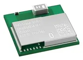


ENW89852A1KF
BLUETOOTH LOW ENERGY MODULE, V5.0
- Manufacturer: PANASONIC
- Product type:
- SVHC: No SVHC (25-Jun-2025)
- Interfaces: I2C, SPI, UART
- Product Range: -
- Certifications: -
- Bluetooth Class: -
- Bluetooth Version: Bluetooth LE 5.0
- Supply Voltage Range: 1.8 V to 3.3 V
- Receiver Sensitivity Rx: -93 dBm
- Operating Temperature Range: -40 °C to 85 °C
| Delivery and price | |
|---|---|
| Units per pack | 250 |
| Price | 6.25 € |
| Current stock | 10+ |
| Lead time | 30 days |
PAN1740A Bluetooth[®] Low Energy Module Product Specification Rev. 0.1 PAN1740A Bluetooth Module **==> picture [302 x 40] intentionally omitted <==** ## ## **Overview** The PAN1740A is an optimized version of the PAN1740, offering a reduced boot time and supporting up to eight connections. It has a fully integrated radio transceiver and baseband processor for Bluetooth[®] 5.0 Low Energy (LE). It can be used as a stand-alone application processor or as a data pump in hosted systems. The device is optimized for remote control units (RCU) requiring support for voice commands and motion/gesture recognition. Its integrated Audio Unit (AU) offers easy interface for MEMS microphones over PDM, external codecs over PCM/I[2] S, and a Sample Rate Converter unit. The Bluetooth LE firmware includes the L2CAP service layer protocols, Security Manager (SM), Attribute Protocol (ATT), the Generic Attribute Profile (GATT), and the Generic Access Profile (GAP). All profiles published by the Bluetooth SIG as well as custom profiles are supported. The transceiver interfaces directly to the antenna and is fully compliant with the Bluetooth 5.0 standard. The PAN1740A has dedicated hardware for the Link Layer implementation of Bluetooth LE and interface controllers for enhanced connectivity capabilities. ## **Features** - [Pre-programmed Bluetooth/MAC address ] - [Includes 16 MHz and 32 768 kHz crystal ] calibrated up to 1 ppm - [Single mode Bluetooth 5.0 System-on-Chip ] - [Programmable ARM][®][ Cortex][®][-M0 CPU ] - [Autonomous Bluetooth LE stand-alone operation ] - [Bluetooth 5.0 (LE) embedded GATT profile (LE ] single mode) - [Dimensions: 9 mm x 9.5 mm x 1.8 mm (SMD ] package with antenna) - [Less than a few µA in low power modes ] - [Integrated shielding to resist EMI ] - [No external components needed ] ## **Characteristics** - [Peak power consumption: 4.9 mA (Rx and Tx) ] - [Link budget: 93 dBm (Rx sensitivity: -93 dBm, ] Tx sensitivity 0 dBm) - [Operating temperature range -40 °C to +85 °C ] ## **Block Diagram** **==> picture [394 x 250] intentionally omitted <==** Product Specification Rev. 0.1 Page 2 PAN1740A Bluetooth Module **==> picture [302 x 40] intentionally omitted <==** By purchase of any of the products described in this document the customer accepts the document's validity and declares their agreement and understanding of its contents and recommendations. Panasonic reserves the right to make changes as required at any time without notification. Please consult the most recently issued Product Specification before initiating or completing a design. © Panasonic Industrial Devices Europe GmbH 2019. This specification sheet is copyrighted. Reproduction of this document is permissible only if reproduction is without alteration and is accompanied by all associated warranties, conditions, limitations, and notices. Do not disclose it to a third party. All rights reserved. This Product Specification does not lodge the claim to be complete and free of mistakes. ## **Engineering Samples (ES)** If Engineering Samples are delivered to the customer, these samples have the status “Engineering Samples”. This means that the design of this product is not yet concluded. Engineering Samples may be partially or fully functional, and they may differ from the published Product Specification. Engineering Samples are not qualified and they are not to be used for reliability testing or series production. ## **Disclaimer** The customer acknowledges that samples may deviate from the Product Specification and may bear defects due to their status of development and the lack of qualification mentioned above. Panasonic rejects any liability or product warranty for Engineering Samples. In particular, Panasonic disclaims liability for damages caused by: - The use of the Engineering Sample other than for evaluation purposes, particularly the installation or integration in another product to be sold by the customer, - Deviation or lapse in function of the Engineering Sample, - Improper use of the Engineering Sample. Panasonic Industrial Devices Europe GmbH disclaims any liability for consequential and incidental damages. In case of any queries regarding the Engineering Samples, please contact your local sales partner or the related product manager. Product Specification Rev. 0.1 Page 3 PAN1740A Bluetooth Module **==> picture [302 x 40] intentionally omitted <==** ## **Table of Contents** |**1**|**About**|**This Document ......................................................................................................................... 5**| |---|---|---| ||1.1|Purpose and Audience .............................................................................................................. 5| ||1.2|Revision History ......................................................................................................................... 5| ||1.3|Use of Symbols ......................................................................................................................... 5| ||1.4|Related Documents ................................................................................................................... 5| |**2**|**Overview .............................................................................................................................................. 6**|| ||2.1|Block Diagram ........................................................................................................................... 7| ||2.2|Bluetooth IC ............................................................................................................................... 8| ||2.3|System Overview ....................................................................................................................... 8| ||2.4|Pin Configuration ..................................................................................................................... 11| ||2.5|Interfaces ................................................................................................................................. 13| |**3**|**Detailed Description ......................................................................................................................... 17**|| ||3.1|Dimensions .............................................................................................................................. 17| ||3.2|Footprint .................................................................................................................................. 18| ||3.3|Packaging ................................................................................................................................ 19| ||3.4|Case Marking .......................................................................................................................... 22| |**4**|**Specification ..................................................................................................................................... 23**|| ||4.1|Default Test Conditions ........................................................................................................... 23| ||4.2|Absolute Maximum Ratings ..................................................................................................... 23| ||4.3|Recommended Operating Conditions ...................................................................................... 24| ||4.4|DC Characteristics ................................................................................................................... 24| ||4.5|16 MHz Crystal Oscillator: Timing Characteristics ................................................................... 25| ||4.6|32 kHz Crystal Oscillator: Timing Characteristics .................................................................... 25| ||4.7|DC-DC Converter: DC Characteristics ..................................................................................... 26| ||4.8|Reliability Tests ....................................................................................................................... 26| ||4.9|Recommended Soldering Profile ............................................................................................. 27| |**5**|**Cautions ............................................................................................................................................ 28**|| ||5.1|Design Notes ........................................................................................................................... 28| ||5.2|Installation Notes ..................................................................................................................... 28| ||5.3|Usage Condition Notes ............................................................................................................ 29| ||5.4|Storage Notes .......................................................................................................................... 29| ||5.5|Safety Cautions ....................................................................................................................... 29| ||5.6|Other Cautions ........................................................................................................................ 30| ||5.7|Restricted Use ......................................................................................................................... 31| |**6**|**Regulatory and Certification Information ....................................................................................... 32**|| |**7**|**Appendix ........................................................................................................................................... 33**|| ||7.1|Ordering Information ................................................................................................................ 33| ||7.2|Contact Details ........................................................................................................................ 34| Product Specification Rev. 0.1 Page 4 PAN1740A Bluetooth Module 1 About This Document ## **1 About This Document** ## **1.1 Purpose and Audience** This Product Specification provides details on the functional, operational, and electrical characteristics of the Panasonic PAN1740A module. It is intended for hardware design, application, and Original Equipment Manufacturer (OEM) engineers. The product is referred to as “the PAN1740A” or “the module” within this document. ## **1.2 Revision History** |**Revision**|**Date**|**Modifications/Remarks**| |---|---|---| |0.1|2019-10-18|Preliminary version| ## **1.3 Use of Symbols** |**Symbol**|**Description**| |---|---| |@|**Note**<br>Indicates important information for the proper use of the product.<br>Non-observance can lead to errors.| |A|**Attention**<br>Indicates important notes that, if not observed, can put the product’s functionality<br>at risk.| |[chapter number]<br>[chapter title]|**Cross reference**<br>Indicates cross references within the document.<br>**Example:**<br>Description of the symbols used in this document1.3 Use of Symbols.| ## **1.4 Related Documents** Please refer to the Panasonic website for related documents 7.2.2 Product Information. Product Specification Rev. 0.1 Page 5 PAN1740A Bluetooth Module 2 Overview **==> picture [302 x 40] intentionally omitted <==** ## **2 Overview** The PAN1740A is an optimized version of the PAN1740, offering a reduced boot time and supporting up to eight connections. It has a fully integrated radio transceiver and baseband processor for Bluetooth 5.0 LE. It can be used as a stand-alone application processor or as a data pump in hosted systems. The device is optimized for remote control units (RCU) requiring support for voice commands and motion/gesture recognition. Its integrated Audio Unit (AU) offers easy interface for MEMS microphones over PDM, external codecs over PCM/I2S, and a Sample Rate Converter unit. The Bluetooth LE firmware includes the L2CAP service layer protocols, Security Manager (SM), Attribute Protocol (ATT), the Generic Attribute Profile (GATT), and the Generic Access Profile (GAP). All profiles published by the Bluetooth SIG as well as custom profiles are supported. The transceiver interfaces directly to the antenna and is fully compliant with the Bluetooth 5.0 standard. The PAN1740A has dedicated hardware for the Link Layer implementation of Bluetooth LE and interface controllers for enhanced connectivity capabilities. For related documents please refer to 7.2.2 Product Information. For further information on the variants and versions please refer to 7.1 Ordering Information. Product Specification Rev. 0.1 Page 6 PAN1740A Bluetooth Module 2 Overview **==> picture [302 x 40] intentionally omitted <==** ## **2.1 Block Diagram** **==> picture [394 x 250] intentionally omitted <==** Total capacity shall not exceed 2.5 µF. The total inductance shall not exceed 2.5 µH. There is no resistor value in this design. Product Specification Rev. 0.1 Page 7 PAN1740A Bluetooth Module 2 Overview ## **2.2 Bluetooth IC** ## **2.3 System Overview** ## **2.3.1 ARM Cortex-M0 CPU** The Cortex-M0 processor is a 32 bit Reduced Instruction Set Computing (RISC) processor with a “von-Neumann-architecture” (single bus interface). It uses an instruction set called “Thumb”, which was first supported in the processor ARM7TDMI. Several newer instructions from the architecture ARMv6 and a few instructions from the Thumb-2 technology are also included. Thumb-2 technology extended the previous Thumb instruction set to allow all operations to be carried out in one CPU state. The instruction set in Thumb-2 includes 16 bit and 32 bit instructions. Most instructions generated by the C compiler use the 16 bit instructions, and the 32 bit instructions are used when the 16 bit version cannot carry out the required operations. This results in high code density and avoids the overhead of switching between two instruction sets. In total, the Cortex-M0 processor supports 56 base instructions, although some instructions can have more than one form. While the instruction set is small, the Cortex-M0 processor is highly capable because the Thumb instruction set is highly optimized. Product Specification Rev. 0.1 Page 8 PAN1740A Bluetooth Module 2 Overview **==> picture [302 x 40] intentionally omitted <==** ## **2.3.2 Bluetooth** ## **Bluetooth LE Core** The Bluetooth LE core is a qualified Bluetooth 5.0 baseband controller compatible with Bluetooth 5.0 specification and it is in charge of packet encoding, decoding, and frame scheduling. - Bluetooth 5.0 specifications compliant according to the specification of the Bluetooth 5.0 System Bluetooth SIG. - All device classes are supported (Broadcast, Central, Observer, Peripheral) - All packet types (Advertising/Data/Control) - Encryption (AES/CCM) - Bit stream processing (CRC, Whitening) - FDMA/TDMA/events formatting and synchronization - Frequency Hopping calculation - Operating clock with internal 16 MHz - Low power modes with internal 32.678 kHz - Supports power down of the baseband during the protocol’s idle periods - Advanced High-Performance Bus (AHB) Slave interface for register file access - AHB Slave interface for exchange memory access of CPU via Bluetooth LE core - AHB Master interface for direct access of Bluetooth LE core to exchange memory space ## **Memory** The following memories are part of the PAN1740A’s internal blocks: - **ROM** - This is a 128 kB ROM containing the Bluetooth 5.0 protocol stack as well as the boot code sequence. • **OTP** This is a 64 kB One-Time-Programmable (OTP) memory array, used to store the application code as well as Bluetooth 5.0 profiles. It also contains the system configuration and calibration data. - **System SRAM** These are four special low leakage SRAM cells, 96 kB in total, which is used for mirroring the program code from the OTP - When the system wakes up, powers up, or mirroring from an external flash, - When the system powers up as well as to store various data of the Bluetooth LE protocol like the system’s global variables, - And processor stack when the system goes into extended sleep mode. Storage of this data ensures secure and quick configuration of the Bluetooth LE Core after the system wakes up. Every cell can be powered on or off according to the application needs for retention area when in extended sleep mode. Product Specification Rev. 0.1 Page 9 PAN1740A Bluetooth Module 2 Overview **==> picture [302 x 40] intentionally omitted <==** ## **Functional Modes** The PAN1740A is optimized for embedded applications such as health monitoring, sports measuring, human interaction devices, etc. Customers are able to develop and test their own applications. Upon completion of development, the application code can be programmed into the OTP. In general, the system has three functional modes of operation: - **Development Mode** During this phase application code is developed using the ARM Cortex-M0 SW environment. The compiled code is downloaded into the System RAM or any retention RAMs by means of SWD (JTAG) or any serial interface (e.g. UART). Address 0x00 is remapped to the physical memory that contains the code and the CPU is configured to reset and execute code from the remapped device. This mode enables application development, debugging and on-the-fly testing. - **Normal Mode** After the application is completed and verified, the code can be burned into the OTP. When the system boots/wakes up, the DMA of the OTP controller will automatically copy the program code from the OTP into the system RAM. Next, a SW reset will remap address 0x00 to the System RAM and code execution is started. Hence, in this mode, the system is autonomous, contains the required SW in OTP and is ready for integration into the final product. - **Calibration Mode** Programming the Bluetooth device address is completed in Calibration mode. ## **Power Modes** There are four different power modes in the PAN1740A: - **Active Mode** System is active and operates at full speed. - **Sleep Mode** No power gating has been programmed, the ARM CPU is idle, waiting for an interrupt. PD_SYS is on. PD_PER and PED_RAD depending on the programmed enabled value. - **Extended Sleep Mode** All power domains are off except for the PD_AON, the programmed PD_RRx and the PD_SR. Since the SysRAM retains its data, no OTP mirroring is required upon waking up the system. - **Deep Sleep Mode** All power domains are off except for the PD_AON and the programmed PD_RRx. This mode dissipates the minimum leakage power. Since the SysRAM has not retained its data, an OTP mirror action is required upon waking up the system. Product Specification Rev. 0.1 Page 10 PAN1740A Bluetooth Module 2 Overview ## **2.4 Pin Configuration** ## **Pin Assignment** **==> picture [247 x 248] intentionally omitted <==** **----- Start of picture text -----**<br> C D<br>A B<br>6 17 15 13<br>20 18 16 14 12<br>21 11<br>22 Top View 10<br>23 9<br>24 2 4 6 8<br>1 3 5 7<br>**----- End of picture text -----**<br> ## **Pin Functions** |**No**|**Pin Name**|**Pin Type**|**Description**| |---|---|---|---| |1 GND|1 GND||| |2 RST|2 RST|I|INPUT| ||||Reset signal (active high)| |3 P0.7|3 P0.7|I/O|General purpose I/O port bit or alternate function nodes| |4 P0.6|4 P0.6|I/O|General purpose I/O port bit or alternate function nodes| |5 P0.5|5 P0.5|I/O|General purpose I/O port bit or alternate function nodes| ||||UART Rx1| |6 P0.4|6 P0.4|I/O|General purpose I/O port bit or alternate function nodes| ||||UART Tx1| 1 Dependent on the software configuration the UART can be set also to any other I/O. Product Specification Rev. 0.1 Page 11 PAN1740A Bluetooth Module 2 Overview **==> picture [302 x 40] intentionally omitted <==** |**No**|**Pin Name**|**Pin Type**|**Description**| |---|---|---|---| ||||| |7|GND||| |8|VBAT3V|AI|Power supply| |9|P0.3|I/O|General purpose I/O port bit or alternate function nodes| ||||UART CTS1| |10|P0.2|I/O|General purpose I/O port bit or alternate function nodes| ||||UART RTS1| |11|P0.1|I/O|General purpose I/O port bit or alternate function nodes| |12|P0.0|I/O|General purpose I/O port bit or alternate function nodes| |13|n.c.||| |14|VDD|AI|INPUT| ||||This pin is used for testing purposes only.| ||||Normal operation: leave VDDfloating| |15|GND||| |16|P1_4/SWCLK|I/O|INPUT JTAG clock signal| |17|GND||| |18|P1_5/SW_DIO|I/O|INPUT/OUTPUT| ||||JTAG Data input/output| |19|GND||| |20|GND||| |21|P1.3|I/O|General purpose I/O port bit or alternate function nodes| |22|P1.2|I/O|General purpose I/O port bit or alternate function nodes| |23|P1.1|I/O|General purpose I/O port bit or alternate function nodes| |24|P1.0|I/O|General purpose I/O port bit or alternate function nodes| |A|GND||| |B|GND||| |C|GND||| |D|GND||| For a more detailed description of the alternate function nodes please refer to the Dialog datasheet 7.2.2 Product Information. Product Specification Rev. 0.1 Page 12 PAN1740A Bluetooth Module 2 Overview **==> picture [302 x 40] intentionally omitted <==** ## **2.5 Interfaces** ## **2.5.1 UART** The UART is compliant to the industry-standard “16550” and is used for serial communication with a peripheral, modem (data carrier equipment [DCE]) or data set. Data is written from a master (CPU) over the APB bus to the UART and it is converted to serial form and transmitted to the destination device. Serial data is also received by the UART and stored for the master (CPU) to read back. There is no DMA support on the UART block since its contains internal FIFOs. Both UARTs support hardware flow control signals (RTS, CTS, DTR, DSR). ## **Features** - 16 bytes Transmit and receive FIFOs - Hardware flow control support (CTS/RTS) - Shadow registers to reduce software overhead and also include a software programmable reset - Transmitter Holding Register Empty (THRE) interrupt mode - IrDA 1.0 SIR mode supporting low power mode ## **Functionality based on the industry standard “16550”** - Programmable character properties, such as number of data bits per character (5, 8), optional - Parity bit (with odd or even select) and number of stop bits (1, 1.5, or 2) - Line break generation and detection - Prioritized interrupt identification - Programmable serial data baud rate as calculated by the following: baud rate = (serial clock frequency)/(divisor). ## **2.5.2 Serial Peripheral Interface (SPI+)** This interface supports a subset of the Serial Peripheral Interface SPI™. The serial interface can transmit and receive, 16 bit or 32 bit in master/slave mode and transmit 9 bit in master mode. The SPI+ interface has enhanced functionality with bidirectional 2x 16 it word FIFOs. SPI is a trademark of Motorola Inc™. ## **Features** - Master/slave mode - 8 bit, 9 bit, 16 bit or 32 bit operation - Clock speeds up to 16 MHz. Programmable output frequencies of SPI source clock divided by 1, 2, 4, 8 - Supports SPI mode 0, 1, 2, 3 (clock edge and phase) - Programmable SPI_DO idle level - Maskable Interrupt generation - Bus load reduction by unidirectional writes-only and reads-only modes - Built-in Rx/Tx FIFOs for continuous SPI bursts Product Specification Rev. 0.1 Page 13 PAN1740A Bluetooth Module 2 Overview **==> picture [302 x 40] intentionally omitted <==** ## **2.5.3 I[2] C** The I[2] C is a programmable control bus that provides support for the communications link between integrated circuits in a system. It is a simple two-wire bus with a software-defined protocol for system control, which is used in temperature sensors and voltage level translators to EEPROMs, general-purpose converters: I/O, A/D, and D/A. ## **Features** - Two-wire I[2] C serial interface consists of a serial data line (SDA) and a serial clock (SCL) - Two speeds are supported: - Standard mode (0 Kb/s to 100 Kb/s) - Fast mode (<= 400 Kb/s) - Clock synchronization - 32 deep transmit/receive FIFOs - Master transmit, Master receive operation - 7 bit or 10 bit addressing - 7 bit or 10 bit combined format transfers - Bulk transmit mode - Default slave address of 0x055 - Interrupt or polled-mode operation - Handles Bit and Byte waiting at both bus speeds - Programmable SDA hold time ## **2.5.4 General Purpose (GP) ADC** The PAN1740A is equipped with a high-speed ultra low power 10 bit general purpose Analog-to-Digital Converter (GPADC). It can operate in unipolar (single ended) mode as well as in bipolar (differential) mode. The ADC has its own voltage regulator (LDO) of 1.2 V, which represents the full scale reference voltage. ## **Features** - 10 bit dynamic ADC with 65 ns conversion time - Maximum sampling rate 3.3 Msample/s - Ultra low power (5 µA typical supply current at 100 ksample/s) - Single-ended as well as differential input with two input scales - Four single-ended or two differential external input channels - Battery monitoring function - Chopper function - Offset and zero scale adjust - Common-mode input level adjust Product Specification Rev. 0.1 Page 14 PAN1740A Bluetooth Module 2 Overview **==> picture [302 x 40] intentionally omitted <==** ## **2.5.5 Quadrature Decoders** This block decodes the pulse trains from a rotary encoder to provide the step and the direction of the movement of an external device. Three axes (X, Y, Z) are supported. The integrated quadrature decoder can automatically decode the signals for the X, Y, and Z axes of a HID input device, reporting step count and direction: the channels are expected to provide a pulse train with 90 degrees phase difference; depending on whether the reference channel is leading or lagging, the direction can be determined. This block can be used for waking up the chip as soon as there is any kind of movement from the external device connected to it. ## **Features** - Three 16 bit signed counters that provide the step count and direction on each of the axes (X, Y, Z) - Programmable system clock sampling at maximum 16 MHz - APB interface for control and programming - Programmable source from the ports: “Port 0”, “Port 1” - Digital filter on the channel inputs to avoid spikes ## **2.5.6 Keyboard Controller** The keyboard controller can be used for debouncing the incoming GPIO signals when implementing a keyboard scanning engine. It generates an interrupt to the CPU (KEYBR_IRQ). In parallel, five extra interrupt lines can be triggered by a state change on 32 selectable GPIOs (GPIOx_IRQ). ## **Features** - Monitors any of the 12 available GPIOs - Generates a keyboard interrupt on key press or key release - Implements de-bouncing time from 0 ms up to 63 ms - Supports five separate interrupt generation lines from GPIO toggling ## **2.5.7 Input/Output Ports** The PAN1740A has software-configurable I/O pin assignment, organized into ports “Port 0” and “Port 1”. ## **Features** - Port 0: 8 pins, Port 1: 6 pins (including SW_CLK and SWDIO) - • Fully programmable pin assignment - Selectable push-pull or open-drain per pin - Selectable 25 KΩ pull-up, pull-down resistors per pin Product Specification Rev. 0.1 Page 15 PAN1740A Bluetooth Module 2 Overview **==> picture [302 x 40] intentionally omitted <==** - Pull-up voltage VBAT3V (buck-mode) - Fixed assignment for analog pin ADC[3:0] - Pins retain their last state when system enters the extended sleep mode or deep sleep mode. ## **2.5.8 Timers** For any software-related description please refer to the according Dialog document. ## **2.5.9 Reset** The PAN1740A comprises an RST pad which is active high. It contains an RC filter for spikes suppression with 400 kΩ and 2.8 pF for the resistor and the capacitor respectively. It also contains a 25 kΩ pull-down resistor. This pad should be connected to ground if not needed by the application. The typical latency of the RST pad is in the range of 2 µs. Product Specification Rev. 0.1 Page 16 PAN1740A Bluetooth Module 3 Detailed Description **==> picture [111 x 17] intentionally omitted <==** **----- Start of picture text -----**<br> <br>**----- End of picture text -----**<br> ## **3 Detailed Description** ## **3.1 Dimensions** **==> picture [30 x 29] intentionally omitted <==** **----- Start of picture text -----**<br> o<br>**----- End of picture text -----**<br> All dimensions are in millimeters. |**No.**|**Item**|**Dimension**|**Tolerance**|**Remark**| |---|---|---|---|---| |1 Width|1 Width|9.50|0.30|0.30| |2 Length|2 Length|9.00|0.30|0.30| |3 Height|3 Height|1.80|0.20 With case|0.20 With case| Product Specification Rev. 0.1 Page 17 PAN1740A Bluetooth Module 3 Detailed Description ## **3.2 Footprint** **==> picture [30 x 29] intentionally omitted <==** **----- Start of picture text -----**<br> @<br>**----- End of picture text -----**<br> - All dimensions are in millimeters. - The outer dimensions have a tolerance of 0.20 mm. - The layout is symetric to center. - The inner pins (2, 4, 6, 9, 11, 14, 16, 18, 21, 23) are shifted to the center by 1 mm. ## Top View **==> picture [366 x 378] intentionally omitted <==** **----- Start of picture text -----**<br> 3.95<br>2.95<br>2.70<br>1.80<br>0.60 0.90<br>C D<br>| A ! B<br>6 17 15 13<br>20 18 16 14 12<br>21 11<br>22 Top View 10<br>ops<br>23 9<br>24 2 4 6 8<br>1 3 5 7<br>9.00<br>1.80<br>0.60<br>1.80<br>9.50<br>0.90<br>1.70 1.80<br>2.70<br>1.00<br>0.55<br>**----- End of picture text -----**<br> Product Specification Rev. 0.1 Page 18 PAN1740A Bluetooth Module 3 Detailed Description ## **3.3 Packaging** The product is a mass production status product and will be delivered in the package described below. ## **3.3.1 Tape Dimensions** **==> picture [390 x 216] intentionally omitted <==** **----- Start of picture text -----**<br> Y<br>—0.30+40.05 6 150-+0.10Do i i ‘ 2.00+0.10 (I) 4.00+0.10 _ (Il) 1.75: +0.10<br>- w w<br>|<br>| % 1.50 min a | | 4<br>X X<br>“| Typ : !<br>j k R0.30<br>Y<br>SECTION Y-<br>Y SCALE 3.5 :<br>1<br>T I AIS? ><br>SECTION X- .<br>X SCALE 3.5 : S<br>Ao 9.90 +/- 0.10 1 S ~~ ><br>(I) Measured from centreline of sprocket hole<br>Bo 9.40 +/- 0.10 SQ e to centreline of pocket.<br>KoK1 2.002.80 +/- 0.10+/- 0.10 Kos Pre e (II) Cumulative tolerance of 10 sprocketholes is ± 0.20 .<br>(III) Measured from centreline of sprocket<br>F 7.50 +/- 0.10 hole to centreline of pocket.<br>P1 12.00 +/- 0.10 Tooling code: Flatbed - 9 (IV) Other material available.<br>W 16.00 +/- 0.30 Estimated Max Length: 72m per 22B3 ALL DIMENSIONS IN MILLIMETRES UNLESS OTHERWISE STATED.<br>**----- End of picture text -----**<br> ## **3.3.2 Packing in Tape** ## Direction of unreeling (for customer) **==> picture [376 x 58] intentionally omitted <==** **----- Start of picture text -----**<br> trailer (empty) component leader (empty) Top cover tape more<br>1 x circumference / packed area minimum 10 pitch than 1 x<br>circumference plus<br>hub standard 100mm to avoid<br>(min 160mm) 1500pcs fixing of tape end on<br>sealed modules.<br>**----- End of picture text -----**<br> Empty spaces in the component packed area shall be less than two per reel and those spaces shall not be consecutive. The top cover tape shall not be found on reel holes and it shall not stick out from the reel. Product Specification Rev. 0.1 Page 19 PAN1740A Bluetooth Module 3 Detailed Description ## **3.3.3 Component Direction** ## **3.3.4 Reel Dimension** Product Specification Rev. 0.1 Page 20 PAN1740A Bluetooth Module 3 Detailed Description ## **3.3.5 Package Label** ## **Example** |(1T)|Lot code| |---|---| |(1P)|Customer order number, if applicable| |(2P)|Order number| |(9D)|Date code| |(Q)|Quantity| |(HW/SW)|Hardware/software version| ## **3.3.6 Total Package** Product Specification Rev. 0.1 Page 21 PAN1740A Bluetooth Module 3 Detailed Description **==> picture [302 x 40] intentionally omitted <==** ## **3.4 Case Marking** tbd Product Specification Rev. 0.1 Page 22 PAN1740A Bluetooth Module 4 Specification ## **4 Specification** All specifications are over temperature and process, unless indicated otherwise. ## **4.1 Default Test Conditions** |Temperature:<br>Humidity:<br>Supply Voltage:|25 °C ± 10 °C<br>40 % to 85 % RH<br>3.3 V| |---|---| ## **4.2 Absolute Maximum Ratings** The maximum ratings may not be exceeded under any circumstances, not even momentarily or individually, as permanent damage to the module may result. **==> picture [30 x 30] intentionally omitted <==** **----- Start of picture text -----**<br> ®@<br>**----- End of picture text -----**<br> The buck mode of the DCDC can operate correctly with voltages in the range of 2.2 V up to 3.3 V. If the voltage drops below, then the OTP might not be readable any more. If no OTP is used, then the system is able to further operate up to 1.8 V. |**Symbol**|**Parameter**|**Condition**|**Min.**|**Typ.**|**Max.**|**Unit**| |---|---|---|---|---|---|---| |VPIN(LIM)<br>(default)|Limiting voltage<br>on a pin|Voltage between GND<br>and VBAT3V|-0.1|-0.1|VBAT3V+<br>0.2|V| |TSTG|Storage<br>temperature||-50|-50|150|°C| |tR(SUP)|Supply rise time Power supply rise time|Supply rise time Power supply rise time|||100|ms| |VBAT(LIM)<br>(VBAT 3V)|Limiting battery<br>supply voltage|Supply voltage on VBAT3V in<br>a buck-converter application,<br>pin VBAT1V is connected to<br>ground|-0.1||3.6|V| |VESD(HBM)|Electrostatic<br>discharge<br>voltage (Human<br>Body Model)||||2 000|V| Product Specification Rev. 0.1 Page 23 PAN1740A Bluetooth Module 4 Specification |**Symbol**|**Parameter**|**Condition**|**Min.**|**Typ.**|**Max.**|**Unit**| |---|---|---|---|---|---|---| |VESD(MM)|Electrostatic<br>discharge<br>voltage<br>(Machine<br>Model)||||175|V| |VESD(CDM)|Electrostatic<br>discharge<br>voltage<br>(Charged<br>Device Model)||||500|V| ## **4.3 Recommended Operating Conditions** The maximum ratings may not be exceeded under any circumstances, not even momentarily or individually, as permanent damage to the module may result. |**Symbol**|**Description**|**Conditions**|**Min.**|**Typ.**|**Max.**|**Unit**| |---|---|---|---|---|---|---| |VBAT(VBAT3V) Battery supply|(VBAT3V) Battery supply<br>voltage||1.8||3.3|V| |VBAT(OTP_P<br>ROG)|Battery supply<br>voltage for otp<br>programming|Supply voltage on VBAT3V<br>for OTP programming|2.25|2.25||V| |VPIN(default)|Voltage on a<br>pin|Voltage between pin and<br>GND|0||Min (3.3<br>VBAT_R<br>F+0.2)|V| |TA|Ambient<br>temperature||-40||85|°C| ## **4.4 DC Characteristics** |**Symbol**|**Description**|**Conditions**|**Min.**|**Typ.**|**Max.**|**Unit**| |---|---|---|---|---|---|---| |IBAT<br>(DP_SLP)_<br>BUCK_0kB|Battery supply<br>current|Typical buck-application in<br>deep-sleep with no<br>retention RAM active.<br>VBAT3V=running from<br>RC32K oscillator||520|520|nA| |IBAT<br>(DP_SLP)_<br>BUCK_16kB|Battery supply<br>current|Typical buck-application in<br>deep-sleep with 16 kB<br>retention RAM active.<br>VBAT3V=3 V||1.2|1.2|µA| Product Specification Rev. 0.1 Page 24 PAN1740A Bluetooth Module 4 Specification **==> picture [302 x 40] intentionally omitted <==** ## |**Symbol**|**Description**|**Conditions**|**Min.**|**Typ.**|**Max.**|**Unit**| |---|---|---|---|---|---|---| |IBAT<br>(EXT_SLP)_<br>BUCK_32kB|Battery supply<br>current|Typical buck-application in<br>extended sleep mode with<br>32 kB retention RAM active.<br>VBAT3V=3 V||1.8||µA| |IBAT<br>(EXT_SLP)<br>_BUCK_64KB|Battery supply<br>current|Typical buck-application in<br>extended sleep mode with<br>64 kB RAM retained,<br>running from XTAL32K<br>oscillator||1.9||µA| |IBAT<br>(EXT_SLP)<br>_BUCK_64kB|Battery supply<br>current|Typical buck-application in<br>extended sleep mode with<br>64 kB RAM retained,<br>running from XTAL32K<br>oscillator||2.9||µA| |IBAT<br>(EXT_SLP)<br>_BUCK_96kB|Battery supply<br>current|Typical buck-application in<br>extended sleep mode with<br>96 kB RAM retained,<br>running from XTAL32K<br>oscillator||4||µA| |IBAT<br>(ACT_RX)_<br>BUCK|Battery supply<br>current|Typical application with<br>buck converter and<br>transmitter active,<br>VBAT3V=3 V||5.3||mA| |IBAT<br>(ACT_TX)_<br>BUCK|Battery supply<br>current|Typical application with<br>buck converter and<br>transmitter active,<br>VBAT3V=3 V||4.9||mA| ## **4.5 16 MHz Crystal Oscillator: Timing Characteristics** |**Symbol**|**Description**|**Conditions**|**Min.**|**Typ.**|**Max.**|**Unit**| |---|---|---|---|---|---|---| |tSTA(XTAL)(16M)|Crystal<br>oscillator<br>startup time||0.5|2|3|ms| ## **4.6 32 kHz Crystal Oscillator: Timing Characteristics** |**Symbol**|**Description**|**Conditions**|**Min.**|**Typ.**|**Max.**|**Unit**| |---|---|---|---|---|---|---| |tSTA(XTAL)(32k)|Crystal<br>oscillator<br>startup time|Typical application, time<br>until 1 000 clocks are<br>detected||0.4||s| Product Specification Rev. 0.1 Page 25 PAN1740A Bluetooth Module 4 Specification **==> picture [302 x 40] intentionally omitted <==** ## **4.7 DC-DC Converter: DC Characteristics** |**Symbol**|**Description**|**Conditions**|**Min.**|**Typ.**|**Max.**|**Unit**| |---|---|---|---|---|---|---| |VO(BUCK)|Output<br>voltage|Default settings||1.41||V| |CONV_MAX<br>(BUCK)|Maximum<br>conversion<br>efficiency|||86||%| |VO/<br>VI(BUCK)|Line<br>regulation|2.35 V<VBAT3V<3.3 V|-2|0.7|2|%/V| |VO/<br>IL(BUCK)|Load<br>regulation|VBAT3V=2.5 V|-0.2|-0.02|0.2|%/mA| |VRPL(BUCK)|Ripple voltage|Buck mode, RMS ripple<br>voltage||2.42||mV| ## **4.8 Reliability Tests** The measurement should be done after the test device has been exposed to room temperature and humidity for one hour. |**No.**|**Item**|**Limit**|**Condition**| |---|---|---|---| |1|Vibration test|Electrical parameter should<br>be in specification|•Freq.: 10 Hz~50 Hz; Amplitude:<br>1.5 mm; 20 min./cycle, 1 h. each of<br>XYZ axis<br>•Freq.: 30 Hz~100 Hz, 6G;<br>20 min./cycle, 1 h. each of XYZ axis| |2|Shock test||Dropped onto hard wood from a height<br>of 50 cm for 3 times| |3|Heat cycle test||-40 °C for 30 min. and +85 °C for 30 min.;<br>each temperature 300 cycles| |4|Moisture test||+60 °C, 90 % RH, 300 h| |5|Low temperature test||-40 °C, 300 h| |6|High temperature test||+85 °C, 300 h| Product Specification Rev. 0.1 Page 26 PAN1740A Bluetooth Module 4 Specification ## **4.9 Recommended Soldering Profile** - Reflow permissible cycles: 2 - Opposite side reflow is prohibited due to module weight - More than 75 percent of the soldering area shall be coated by solder - The soldering profiles should be adhered to in order to prevent electrical or mechanical damage - Soldering profile assumes lead-free soldering Product Specification Rev. 0.1 Page 27 PAN1740A Bluetooth Module 5 Cautions ## **5 Cautions** Failure to follow the guidelines set forth in this document may result in degrading of the product’s functions and damage to the product. ## **5.1 Design Notes** 1. Follow the conditions written in this specification, especially the control signals of this module. 2. The supply voltage should abide by the maximum ratings ( 4.2 Absolute Maximum Ratings). 3. The supply voltage must be free of AC ripple voltage (for example from a battery or a low noise regulator output). For noisy supply voltages, provide a decoupling circuit (for example a ferrite in series connection and a bypass capacitor to ground of at least 47 µF directly at the module). 4. This module should not be mechanically stressed when installed. 5. Keep this module away from heat. Heat is the major cause of decreasing the life time of these modules. 6. Avoid assembly and use of the target equipment in conditions where the module temperature may exceed the maximum tolerance. 7. Keep this module away from other high frequency circuits. 8. Refer to the recommended pattern when designing a board. ## **5.2 Installation Notes** 1. Reflow soldering is possible twice based on the conditions set forth in 4.9 Recommended Soldering Profile. Set up the temperature at the soldering portion of this module according to this reflow profile. 2. Carefully position the module so that the heat will not burn into printed circuit boards or affect other components that are susceptible to heat. 3. Carefully locate the module, to avoid an increased temperature caused by heat generated by neighboring components. 4. If a vinyl-covered wire comes into contact with the module, the wire cover will melt and generate toxic gas, damaging the insulation. Never allow contact between a vinyl cover and these modules to occur. 5. This module should not be mechanically stressed or vibrated when reflowed. 6. To repair the board by hand soldering, follow the conditions set forth in this chapter. 7. Do not wash this product. 8. Pressing on parts of the metal cover or fastening objects to the metal will cause damage to the module. Product Specification Rev. 0.1 Page 28 PAN1740A Bluetooth Module 5 Cautions **==> picture [302 x 40] intentionally omitted <==** ## **5.3 Usage Condition Notes** 1. Take measures to protect the module against static electricity. If pulses or transient loads (a large load, which is suddenly applied) are applied to the modules, check and evaluate their operation before assembly of the final products. 2. Do not use dropped modules. 3. Do not touch, damage, or soil the pins. 4. Follow the recommended condition ratings about the power supply applied to this module. 5. Electrode peeling strength: Do not apply a force of more than 4.9 N in any direction on the soldered module. 6. Pressing on parts of the metal cover or fastening objects to the metal cover will cause damage. 7. These modules are intended for general purpose and standard use in general electronic equipment, such as home appliances, office equipment, information, and communication equipment. ## **5.4 Storage Notes** 1. The module should not be stressed mechanically during storage. 2. Do not store these modules in the following conditions or the performance characteristics of the module, such as RF performance will be adversely affected: - Storage in salty air or in an environment with a high concentration of corrosive gas, such as Cl2, H2S, NH3, SO2, or NOX, - Storage in direct sunlight, - Storage in an environment where the temperature may be outside the range of 5 °C to 35 °C, or where the humidity may be outside the 45 percent to 85 percent range, - Storage of the modules for more than one year after the date of delivery storage period: Please check the adhesive strength of the embossed tape and soldering after 6 months of storage. 3. Keep this module away from water, poisonous gas, and corrosive gas. 4. This module should not be stressed or shocked when transported. 5. Follow the specification when stacking packed crates (max. 10). ## **5.5 Safety Cautions** These specifications are intended to preserve the quality assurance of products and individual components. Before use, check and evaluate the operation when mounted on your products. Abide by these specifications without deviation when using the products. These products may short-circuit. If electrical shocks, smoke, fire, and/or accidents involving human life are anticipated when a short circuit occurs, provide the following failsafe functions as a minimum: Product Specification Rev. 0.1 Page 29 PAN1740A Bluetooth Module 5 Cautions 1. Ensure the safety of the whole system by installing a protection circuit and a protection device. 2. Ensure the safety of the whole system by installing a redundant circuit or another system to prevent a single fault causing an unsafe status. ## **5.6 Other Cautions** 1. Do not use the module for other purposes than those listed in section 5.3 Usage Condition Notes. 2. Be sure to provide an appropriate fail-safe function on your product to prevent any additional damage that may be caused by the abnormal function or the failure of the module. 3. This module has been manufactured without any ozone chemical controlled under the Montreal Protocol. 4. These modules are not intended for use under the special conditions shown below. Before using these modules under such special conditions, carefully check their performance and reliability under the said special conditions to determine whether or not they can be used in such a manner: - In liquid, such as water, salt water, oil, alkali, or organic solvent, or in places where liquid may splash, - In direct sunlight, outdoors, or in a dusty environment, - In an environment where condensation occurs, - In an environment with a high concentration of harmful gas (e.g. salty air, HCl, Cl2, SO2, H2S, NH3, and NOX). 5. If an abnormal voltage is applied due to a problem occurring in other components or circuits, replace these modules with new modules, because they may not be able to provide normal performance even if their electronic characteristics and appearances appear satisfactory. | Please refer to the Panasonic website for further information 7.2.2 Product Information. Product Specification Rev. 0.1 Page 30 PAN1740A Bluetooth Module 5 Cautions **==> picture [302 x 40] intentionally omitted <==** ## **5.7 Restricted Use** ## **5.7.1 Life Support Policy** This Panasonic Industrial Devices Europe GmbH product is not designed for use in life support appliances, devices, or systems where malfunction can reasonably be expected to result in a significant personal injury to the user, or as a critical component in any life support device or system whose failure to perform can be reasonably expected to cause the failure of the life support device or system, or to affect its safety or effectiveness. Panasonic customers using or selling these products for use in such applications do so at their own risk and agree to fully indemnify Panasonic Industrial Devices Europe GmbH for any damages resulting. ## **5.7.2 Restricted End Use** This Panasonic Industrial Devices Europe GmbH product is not designed for any restricted activity that supports the development, production, handling usage, maintenance, storage, inventory or proliferation of any weapons or military use. Transfer, export, re-export, usage or reselling of this product to any destination, end user or any end use prohibited by the European Union, United States or any other applicable law is strictly prohibited. Product Specification Rev. 0.1 Page 31 PAN1740A Bluetooth Module **==> picture [302 x 40] intentionally omitted <==** 6 Regulatory and Certification Information ## **6 Regulatory and Certification Information** tbd Product Specification Rev. 0.1 Page 32 PAN1740A Bluetooth Module 7 Appendix **==> picture [302 x 40] intentionally omitted <==** ## **7 Appendix** ## **7.1 Ordering Information** ## **Variants and Versions** |**Order Number**|**Brand Name**|**Description**|**MOQ**| |---|---|---|---| |ENW89852A1KF2|PAN1740A|PAN1740A Bluetooth Low Energy<br>Module|1 500| ## **Evaluation Tools[3]** |**Order Number**|**Tool Name**|**Content**|**MOQ3**| |---|---|---|---| |ENW89852AWKF|PAN1740A Kit|2x USB-Stick|1| |ENW89852AXKF|PAN1740A ETU|USB-Stick|1| |ENW89852AUKF|PAN1740A Daughter Board|PAN1740A Daughter board|1| |ENW89852AVKF|PAN1740A Dialog Pro Kit|•Dialog Pro Kit (Motherboard)<br>•3x PAN1740A Daughter Board<br>•USB-Stick<br>•USB-Cable<br>• Battery|1| > 2 Samples are available on customer demand. > 3 Please refer to the Panasonic website for further information 7.2.2 Product Information. Product Specification Rev. 0.1 Page 33 PAN1740A Bluetooth Module 7 Appendix **==> picture [302 x 40] intentionally omitted <==** ## **7.2 Contact Details** ## **7.2.1 Contact Us** Please contact your local Panasonic Sales office for details on additional product options and services: For Panasonic Sales assistance in the **EU** , visit https://eu.industrial.panasonic.com/about-us/contact-us Email: wireless@eu.panasonic.com For Panasonic Sales assistance in **North America** , visit the Panasonic Sales & Support Tool to find assistance near you at https://na.industrial.panasonic.com/distributors Please visit the **Panasonic Wireless Technical Forum** to submit a question at https://forum.na.industrial.panasonic.com ## **7.2.2 Product Information** Please refer to the Panasonic Wireless Connectivity website for further information on our products and related documents: For complete Panasonic product details in the **EU** , visit http://pideu.panasonic.de/products/wireless-modules.html For complete Panasonic product details in **North America** , visit http://www.panasonic.com/rfmodules Product Specification Rev. 0.1 Page 34
Updated at March 30, 2026
Panasonic Industry is a global leader in the design and manufacture of high-quality electronic components. Renowned for a commitment to continuous innovation, the company provides the essential building blocks that empower modern engineering. From industrial automation to consumer electronics, Panasonic's components are trusted worldwide for their outstanding reliability, efficiency, and long-term performance. The extensive portfolio is anchored by a massive selection of passive components, featuring an industry-leading range of aluminium electrolytic, film, and polymer capacitors. Alongside these advanced capacitance solutions, engineers rely on Panasonic's robust power inductors and a highly versatile array of electromechanical devices, including solid-state, power, and signal relays engineered to excel in demanding environments. Beyond core passives and switching solutions, the offering encompasses critical circuit protection devices such as TVS varistors and NTC thermistors, as well as sophisticated thermal management materials. Panasonic also delivers precision light and motion sensors, highly reliable batteries, and advanced Bluetooth and WLAN connectivity modules, providing a comprehensive ecosystem of components to support next-generation technological design.
About Novapart
Novapart is a B2B electronic component broker specialising in stock shortages and cost reduction. We source hard-to-find parts and identify compliant alternatives across a catalogue of 410,000+ components from 500+ manufacturers.
Learn more →Stock Shortage Specialist
When a component is unavailable, discontinued or has an unacceptable lead time, we tap into our network of vetted European and Asian distributors to source what you need — without compromising on quality or traceability.
Request a quote →Compliant Alternatives
We identify pin-to-pin, electrically equivalent substitutes that meet the same certifications (RoHS, AEC-Q100, REACH) as your original specification — validated against datasheets, not just part numbers. Often at a lower cost.
BOM Analysis service →